 | –≠–ª–µ–∫—Ç—Ä–æ–Ω–Ω—ã–π –∫–æ–º–ø–æ–Ω–µ–Ω—Ç: MAX5891 | –°–∫–∞—á–∞—Ç—å:  PDF PDF  ZIP ZIP |

General Description
The MAX5891 advanced 16-bit, 600Msps, digital-to-
analog converter (DAC) meets the demanding perfor-
mance requirements of signal synthesis applications
found in wireless base stations and other communica-
tions applications. Operating from +3.3V and +1.8V
supplies, the MAX5891 DAC supports update rates of
600Msps using high-speed LVDS inputs while consum-
ing only 298mW of power and offers exceptional
dynamic performance such as 80dBc spurious-free
dynamic range (SFDR) at f
OUT
= 30MHz.
The MAX5891 utilizes a current-steering architecture that
supports a 2mA to 20mA full-scale output current range,
and produces -2dBm to -22dBm full-scale output signal
levels with a double-terminated 50
load. The MAX5891
features an integrated +1.2V bandgap reference and
control amplifier to ensure high-accuracy and low-noise
performance. A separate reference input (REFIO) allows
for the use of an external reference source for optimum
flexibility and improved gain accuracy.
The MAX5891 digital inputs accept LVDS voltage lev-
els, and the flexible clock input can be driven differen-
tially or single-ended, AC- or DC-coupled. The
MAX5891 is available in a 68-pin QFN package with an
exposed paddle (EP) and is specified for the extended
(-40∞C to +85∞C) temperature range.
Refer to the MAX5890* and MAX5889* data sheets for
pin-compatible 14-bit and 12-bit versions of the
MAX5891.
Applications
Base Stations: Single/Multicarrier UMTS,
CDMA, GSM
Communications: Fixed Broadband Wireless
Access, Point-to-Point Microwave
Direct Digital Synthesis (DDS)
Cable Modem Termination Systems (CMTS)
Automated Test Equipment (ATE)
Instrumentation
Features
600Msps Output Update Rate
Low Noise Spectral Density: -163dBFS/Hz at
f
OUT
= 36MHz
Excellent SFDR and IMD Performance
SFDR = 80dBc at f
OUT
= 30MHz (to Nyquist)
SFDR = 69dBc at f
OUT
= 130MHz (to Nyquist)
IMD = -94dBc at f
OUT
= 30MHz
IMD = -77dBc at f
OUT
= 130MHz
ACLR = 73dB at f
OUT
= 122.88MHz
2mA to 20mA Full-Scale Output Current
LVDS-Compatible Digital Inputs
On-Chip +1.2V Bandgap Reference
Low 298mW Power Dissipation at 600Msps
Compact (10mm x 10mm) QFN-EP Package
Evaluation Kit Available (MAX5891EVKIT)
MAX5891
16-Bit, 600Msps, High-Dynamic-Performance
DAC with LVDS Inputs
________________________________________________________________ Maxim Integrated Products
1
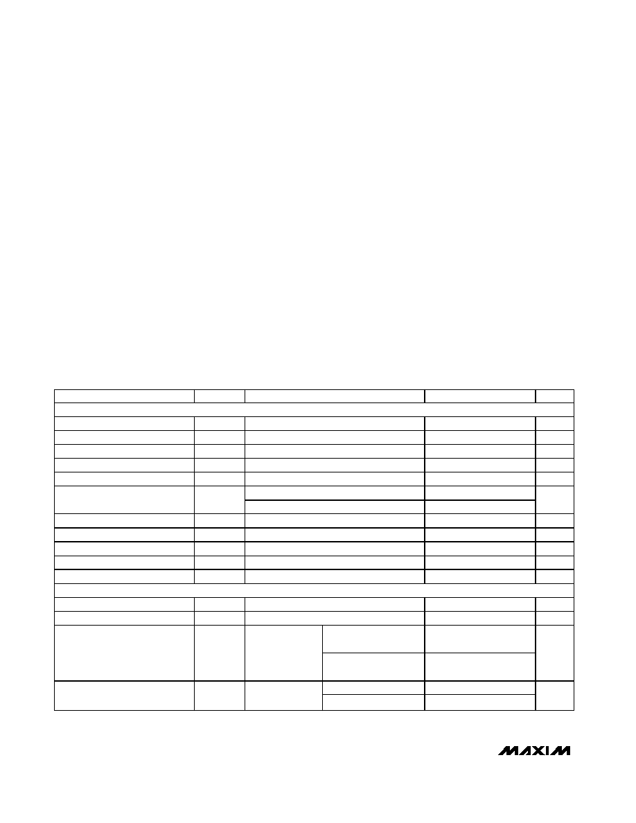
Ordering Information
19-3542; Rev 0; 2/05
For pricing, delivery, and ordering information, please contact Maxim/Dallas Direct! at
1-888-629-4642, or visit Maxim's website at www.maxim-ic.com.
EVALUATION KIT
AVAILABLE
PART
TEMP RANGE
PIN-PACKAGE
PKG
CODE
MAX5891EGK
-40
∞C to +85∞C 68 QFN-EP**
G6800-4
MAX5891
+1.2V
REFERENCE
REFIO
DACREF
FSADJ
CLK
INTERFACE
600MHz
16-BIT DAC
LATCH
LVDS
RECEIVER
D0≠D15
LVDS DATA
INPUTS
POWER
DOWN
PD
CLKP
CLKN
OUTP
OUTN
Functional Diagram
PART
RESOLUTION
(BITS)
UPDATE RATE
(Msps)
LOGIC INPUT
MAX5889*
12
600
LVDS
MAX5890*
14
600
LVDS
MAX5891
16
600
LVDS
Selector Guide
*Future product--contact factory for availability.
**EP = Exposed paddle.
Pin Configuration appears at end of data sheet.
MAX5891
16-Bit, 600Msps, High-Dynamic-Performance
DAC with LVDS Inputs
2
_______________________________________________________________________________________
ABSOLUTE MAXIMUM RATINGS
ELECTRICAL CHARACTERISTICS
(AV
DD3.3
= DV
DD3.3
= AV
CLK
= +3.3V, AV
DD1.8
= DV
DD1.8
= +1.8V, external reference V
REFIO
= +1.2V, output load 50
double-ter-
minated, transformer-coupled output, I
OUT
= 20mA, T
A
= -40∞C to +85∞C, unless otherwise noted. Specifications at T
A
+25∞C are
guaranteed by production testing. Specifications at T
A
< +25∞C are guaranteed by design and characterization. Typical values are at
T
A
= +25∞C.)
Stresses beyond those listed under "Absolute Maximum Ratings" may cause permanent damage to the device. These are stress ratings only, and functional
operation of the device at these or any other conditions beyond those indicated in the operational sections of the specifications is not implied. Exposure to
absolute maximum rating conditions for extended periods may affect device reliability.
AV
DD1.8
, DV
DD1.8
to AGND, DGND, DACREF,
and CGND.......................................................-0.3V to +2.16V
AV
DD3.3
, DV
DD3.3
, AV
CLK
to AGND, DGND,
DACREF, and CGND.........................................-0.3V to +3.9V
REFIO, FSADJ to AGND, DACREF,
DGND, and CGND ..........................-0.3V to (AV
DD3.3
+ 0.3V)
OUTP, OUTN to AGND, DGND, DACREF,
and CGND .......................................-1.2V to (AV
DD3.3
+ 0.3V)
CLKP, CLKN to AGND, DGND, DACREF,
and CGND..........................................-0.3V to (AV
CLK
+ 0.3V)
PD to AGND, DGND, DACREF,
and CGND.......................................-0.3V to (DV
DD3.3
+ 0.3V)
Digital Data Inputs (D0N≠D15N, D0P≠D15P) to AGND,
DGND, DACREF, and CGND ..........-0.3V to (DV
DD1.8
+ 0.3V)
Continuous Power Dissipation (T
A
= +70∞C) (Note 1)
68-Pin QFN-EP (derate 28.6mW/∞C above +70∞C)....3333mW
Thermal Resistance
JA
(Note 1) ....................................24∞C/W
Operating Temperature Range ..........................-40∞C to +85∞C
Junction Temperature .....................................................+150∞C
Storage Temperature Range ............................-60∞C to +150∞C
Lead Temperature (soldering, 10s) ................................+300∞C
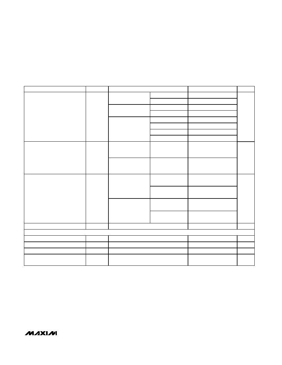
PARAMETER
SYMBOL
CONDITIONS
MIN
TYP
MAX
UNITS
STATIC PERFORMANCE
Resolution
16
Bits
Integral Nonlinearity
INL
Measured differentially
±3.8
LSB
Differential Nonlinearity
DNL
Measured differentially
±1.6
LSB
Offset Error
OS
-0.02
±0.001
+0.02
%FS
Full-Scale Gain Error
GE
FS
External reference
-4
±1
+4
%FS
Internal reference
±130
Gain-Drift Tempco
External reference
±100
ppm/
∞C
Full-Scale Output Current
I
OUT
2
20
mA
Output Compliance
Single-ended
-1.0
+1.1
V
Output Resistance
R
OUT
1
M
Output Capacitance
C
OUT
5
pF
Output Leakage Current
PD = high, power-down mode
±1
µA
DYNAMIC PERFORMANCE
Maximum DAC Update Rate
600
Msps
Minimum DAC Update Rate
1
Msps
f
OUT
= 36MHz
A
FULL-SCALE
= -3.5dBm
-163
Noise Spectral Density
N
f
CLK
= 500MHz,
-12dBFS, 20MHz
offset from the
carrier
f
OUT
= 151MHz
A
FULL-SCALE
= -6.4dBm
-155
dBFS/Hz
f
OUT
= 36MHz
70
Signal-to-Noise Ratio Over
Nyquist
SNR
f
CLK
= 500MHz,
0dBFS
f
OUT
= 151MHz
64
dB
Note 1: Thermal resistance based on a multilayer board with 4x4 via array in exposed paddle area
MAX5891
16-Bit, 600Msps, High-Dynamic-Performance
DAC with LVDS Inputs
_______________________________________________________________________________________
3
ELECTRICAL CHARACTERISTICS (continued)
(AV
DD3.3
= DV
DD3.3
= AV
CLK
= +3.3V, AV
DD1.8
= DV
DD1.8
= +1.8V, external reference V
REFIO
= +1.2V, output load 50
double-ter-
minated, transformer-coupled output, I
OUT
= 20mA, T
A
= -40∞C to +85∞C, unless otherwise noted. Specifications at T
A
+25∞C are
guaranteed by production testing. Specifications at T
A
< +25∞C are guaranteed by design and characterization. Typical values are at
T
A
= +25∞C.)
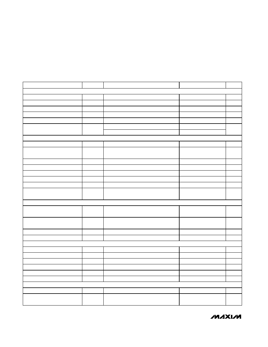
PARAMETER
SYMBOL
CONDITIONS
MIN
TYP
MAX
UNITS
f
OUT
= 16MHz
86
f
CLK
= 200MHz,
0dBFS
f
OUT
= 30MHz
84
f
OUT
= 16MHz
76
f
CLK
= 200MHz,
-12dBFS
f
OUT
= 30MHz
76
f
OUT
= 16MHz
77
84
f
OUT
= 30MHz
80
f
OUT
= 130MHz
69
Spurious-Free
Dynamic Range to
Nyquist
SFDR
f
CLK
= 500MHz,
0dBFS
f
OUT
= 200MHz
63
dBc
f
CLK
= 500MHz
f
OUT1
= 29MHz,
f
OUT2
= 30MHz,
-6.5dBFS per tone
-94
Two-Tone IMD
TTIMD
f
CLK
= 500MHz
f
OUT1
= 129MHz,
f
OUT2
= 130MHz,
-6.5dBFS per tone
-77
dBc
f
CLK
= 491.52MHz,
f
OUT
= 30.72MHz
82
WCDMA single
carrier
f
CLK
= 491.52MHz,
f
OUT
= 122.88MHz
73
f
CLK
= 491.52MHz,
f
OUT
= 30.72MHz
74
Adjacent Channel
Leakage Power Ratio
ACLR
WCDMA four carriers
f
CLK
= 491.52MHz,
f
OUT
= 122.88MHz
67
dB
Output Bandwidth
BW
-1dB
(Note 2)
1000
MHz
REFERENCE
Internal Reference Voltage Range
V
REFIO
1.14
1.2
1.26
V
Reference Input Voltage Range
V
REFIOCR
Using external reference
0.10
1.2
1.32
V
Reference Input Resistance
R
REFIO
10
k
Reference Voltage Temperature
Drift
TCO
REF
±50
ppm/
∞C
MAX5891
16-Bit, 600Msps, High-Dynamic-Performance
DAC with LVDS Inputs
4
_______________________________________________________________________________________
ELECTRICAL CHARACTERISTICS (continued)
(AV
DD3.3
= DV
DD3.3
= AV
CLK
= +3.3V, AV
DD1.8
= DV
DD1.8
= +1.8V, external reference V
REFIO
= +1.2V, output load 50
double-ter-
minated, transformer-coupled output, I
OUT
= 20mA, T
A
= -40∞C to +85∞C, unless otherwise noted. Specifications at T
A
+25∞C are
guaranteed by production testing. Specifications at T
A
< +25∞C are guaranteed by design and characterization. Typical values are at
T
A
= +25∞C.)
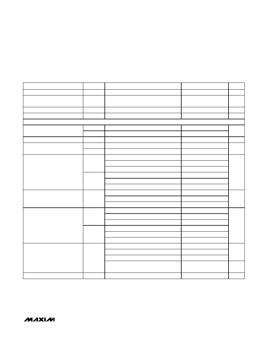
PARAMETER
SYMBOL
CONDITIONS
MIN
TYP
MAX
UNITS
ANALOG OUTPUT TIMING (Figure 3)
Output Fall Time
t
FALL
90% to 10% (Note 3)
0.4
ns
Output Rise Time
t
RISE
10% to 90% (Note 3)
0.4
ns
Output Propagation Delay
t
PD
Reference to data latency (Note 3)
2.5
ns
Output Settling Time
To 0.025% of the final value (Note 3)
11
ns
Glitch Impulse
Measured differentially
1
pV
∑
s
I
OUT
= 2mA
30
Output Noise
N
OUT
I
OUT
= 20mA
30
pA/
Hz
TIMING CHARACTERISTICS
Input Data Rate
600
MWps
Data Latency
5.5
Clock
cycles
Data to Clock Setup Time
t
SETUP
Referenced to rising edge of clock (Note 4)
-1.2
ns
Data to Clock Hold Time
t
HOLD
Referenced to rising edge of clock (Note 4)
2
ns
Clock Frequency
f
CLK
CLKP, CLKN
600
MHz
Minimum Clock Pulse-Width High
t
CH
CLKP, CLKN
0.6
ns
Minimum Clock Pulse-Width Low
t
CL
CLKP, CLKN
0.6
ns
Turn-On Time
t
SHDN
External reference, PD falling edge to
output settle within 1%
350
µs
CMOS LOGIC INPUT (PD)
Input Logic High
V
IH
0.7 x
DV
DD3.3
V
Input Logic Low
V
IL
0.3 x
DV
DD3.3
V
Input Current
I
IN
-5
±1.8
+5
µA
Input Capacitance
C
IN
3
pF
LVDS INPUTS
Differential Input High
V
IHLVDS
+100
mV
Differential Input Low
V
ILLVDS
-100
mV
Common-Mode Voltage Range
V
ICMLVDS
1.125
1.375
V
Differential Input Resistance
R
IDLVDS
110
Common-Mode Input Resistance
R
ICMLVDS
3.2
k
Input Capacitance
C
INLVDS
3
pF
DIFFERENTIAL CLOCK INPUTS (CLKP, CLKN)
Clock Common-Mode Voltage
CLKP and CLKN are internally biased
AV
CLK
/ 2
V
Minimum Differential Input
Voltage Swing
0.5
V
P-P
MAX5891
16-Bit, 600Msps, High-Dynamic-Performance
DAC with LVDS Inputs
_______________________________________________________________________________________
5
Note 2: This parameter does not include update-rate-dependent effects of sin(x)/x filtering inherent in the MAX5891.
Note 3: Parameter measured single-ended with 50
double-terminated outputs.
Note 4: Not production tested. Guaranteed by design.
Note 5: Parameter defined as the change in midscale output caused by a
±5% variation in the nominal supply voltages.
ELECTRICAL CHARACTERISTICS (continued)
(AV
DD3.3
= DV
DD3.3
= AV
CLK
= +3.3V, AV
DD1.8
= DV
DD1.8
= +1.8V, external reference V
REFIO
= +1.2V, output load 50
double-ter-
minated, transformer-coupled output, I
OUT
= 20mA, T
A
= -40∞C to +85∞C, unless otherwise noted. Specifications at T
A
+25∞C are
guaranteed by production testing. Specifications at T
A
< +25∞C are guaranteed by design and characterization. Typical values are at
T
A
= +25∞C.)
PARAMETER
SYMBOL
CONDITIONS
MIN
TYP
MAX
UNITS
Minimum Common-Mode Voltage
1
V
Maximum Common-Mode
Voltage
1.9
V
Input Resistance
R
CLK
Single-ended
5
k
Input Capacitance
C
CLK
3
pF
POWER SUPPLIES
AV
DD3.3
3.135
3.3
3.465
Analog Supply Voltage Range
AV
DD1.8
1.710
1.8
1.890
V
Clock Supply Voltage Range
AV
CLK
3.135
3.3
3.465
V
DV
DD3.3
3.135
3.3
3.465
Digital Supply Voltage Range
DV
DD1.8
1.710
1.8
1.890
V
f
CLK
= 100MHz, f
OUT
= 16MHz
26.5
f
CLK
= 500MHz, f
OUT
= 16MHz
26.5
28
I
AVDD3.3
f
CLK
= 600MHz, f
OUT
= 16MHz
26.5
f
CLK
= 100MHz, f
OUT
= 16MHz
11.3
f
CLK
= 500MHz, f
OUT
= 16MHz
50
58
Analog Supply Current
I
AVDD1.8
f
CLK
= 600MHz, f
OUT
= 16MHz
61
mA
f
CLK
= 100MHz, f
OUT
= 16MHz
2.8
f
CLK
= 500MHz, f
OUT
= 16MHz
2.8
3.6
Clock Supply Current
I
AVCLK
f
CLK
= 600MHz, f
OUT
= 16MHz
2.8
mA
f
CLK
= 100MHz, f
OUT
= 16MHz
0.2
f
CLK
= 500MHz, f
OUT
= 16MHz
0.2
0.5
I
DVDD3.3
f
CLK
= 600MHz, f
OUT
= 16MHz
0.2
f
CLK
= 100MHz, f
OUT
= 16MHz
10.6
f
CLK
= 500MHz, f
OUT
= 16MHz
44
50
Digital Supply Current
I
DVDD1.8
f
CLK
= 600MHz, f
OUT
= 16MHz
50.5
mA
f
CLK
= 100MHz, f
OUT
= 16MHz
137
f
CLK
= 500MHz, f
OUT
= 16MHz
267
301
f
CLK
= 600MHz, f
OUT
= 16MHz
298
mW
Total Power Dissipation
P
DISS
Power-down, clock static low,
data input static
13
µW
Power-Supply Rejection Ratio
PSRR
(Note 5)
±0.025
%FS