 | –≠–ª–µ–∫—Ç—Ä–æ–Ω–Ω—ã–π –∫–æ–º–ø–æ–Ω–µ–Ω—Ç: MAX5893 | –°–∫–∞—á–∞—Ç—å:  PDF PDF  ZIP ZIP |
General Description
The MAX5893 programmable interpolating, modulating,
500Msps, dual digital-to-analog converter (DAC) offers
superior dynamic performance and is optimized for high-
performance wideband, single-carrier transmit applica-
tions. The device integrates a selectable 2x/4x/8x
interpolating filter, a digital quadrature modulator, and
dual 12-bit high-speed DACs on a single integrated cir-
cuit. At 30MHz output frequency and 500Msps update
rate, the in-band SFDR is 84dBc while consuming 1.1W.
The device also delivers 72dB ACLR for single-carrier
WCDMA at a 61.44MHz output frequency.
The selectable interpolating filters allow lower input data
rates while taking advantage of the high DAC update
rates. These linear-phase interpolation filters ease
reconstruction filter requirements and enhance the
passband dynamic performance. Individual offset and
gain programmability allow the user to calibrate out local
oscillator (LO) feedthrough and sideband suppression
errors generated by analog quadrature modulators.
The MAX5893 features a f
IM
/ 4 digital image-reject
modulator. This modulator generates a quadrature-mod-
ulated IF signal that can be presented to an analog I/Q
modulator to complete the upconversion process. A
second digital modulation mode allows the signal to be
frequency-translated with image pairs at f
IM
/ 2 or f
IM
/ 4.
The MAX5893 features a standard 1.8V CMOS, 3.3V tol-
erant data input bus for easy interface. A 3.3V SPITM port
is provided for mode configuration. The programmable
modes include the selection of 2x/4x/8x interpolating fil-
ters, f
IM
/ 2, f
IM
/ 4 or no digital quadrature modulation
with image rejection, channel gain and offset adjustment,
and offset binary or two's complement data interface.
Pin-compatible 14- and 16-bit devices are also available.
Refer to the MAX5894** data sheet for the 14-bit version
and the MAX5895 data sheet for the 16-bit version.
Applications
Base Stations: 3G UMTS, CDMA, and GSM
Broadband Wireless Transmitters
Broadband Cable Infrastructure
Instrumentation and Automatic Test Equipment (ATE)
Analog Quadrature Modulation Architectures
Features
72dB ACLR at f
OUT
= 61.44MHz (Single-Carrier
WCDMA)
Meets 3G UMTS, cdma2000
Æ
, GSM Spectral Masks
(f
OUT
= 122MHz)
Noise Spectral Density = -151dBFS/Hz at
f
OUT
= 16MHz
90dBc SFDR at Low-IF Frequency (10MHz)
86dBc SFDR at High-IF Frequency (50MHz)
Low Power: 511mW (f
CLK
= 100MHz)
User Programmable
Selectable 2x, 4x, or 8x Interpolating Filters
<0.01dB Passband Ripple
>99dB Stopband Rejection
Selectable Real or Complex Modulator Operation
Selectable Modulator LO Frequency: OFF, f
IM
/ 2,
or f
IM
/ 4
Selectable Output Filter: Lowpass or Highpass
Channel Gain and Offset Adjustment
EV Kit Available (Order the MAX5895EVKIT)
MAX5893
12-Bit, 500Msps Interpolating and Modulating
Dual DAC with CMOS Inputs
________________________________________________________________ Maxim Integrated Products
1
PART
RESOLUTION
(BITS)
DAC UPDATE
RATE (Msps)
INPUT
LOGIC
MAX5893
12
500
CMOS
MAX5894**
14
500
CMOS
MAX5895
16
500
CMOS
PART
TEMP RANGE
PIN-PACKAGE
PKG
CODE
MAX5893EGK
-40∞C to +85∞C
68 QFN-EP*
(10mm x 10mm)
G6800-4
Selector Guide
Ordering Information
DA
T
A
SYNCH
AND DEMUX
DAC
DATA
PORT A
DATA
PORT B
DATACLK
OUTI
OUTQ
MODULA
TOR
2x
INTERPOLA
TING
FIL
TERS
1x/2x/4x
INTERPOLA
TING
FIL
TERS
DAC
Simplified Diagram
19-3546; Rev 0; 2/05
For pricing, delivery, and ordering information, please contact Maxim/Dallas Direct! at
1-888-629-4642, or visit Maxim's website at www.maxim-ic.com.
Pin Configuration appears at end of data sheet.
SPI is a trademark of Motorola, Inc.
cdma2000 is a registered trademark of Telecommunications
Industry Association.
**Future product--contact factory for availability.
*EP = Exposed paddle.
EVALUATION KIT
AVAILABLE
MAX5893
12-Bit, 500Msps Interpolating and Modulating
Dual DAC with CMOS Inputs
2
_______________________________________________________________________________________
ABSOLUTE MAXIMUM RATINGS
ELECTRICAL CHARACTERISTICS
(DV
DD1.8
= AV
DD1.8
= 1.8V, AV
CLK
= AV
DD3.3
= DV
DD3.3
= 3.3V, modulator off, 2x interpolation, DATACLK input mode, dual-port
mode, 50
double-terminated outputs, external reference at 1.25V, T
A
= -40∞C to +85∞C, unless otherwise noted. Typical values are
at T
A
= +25∞C, unless otherwise noted.) (Note 2)
Stresses beyond those listed under "Absolute Maximum Ratings" may cause permanent damage to the device. These are stress ratings only, and functional
operation of the device at these or any other conditions beyond those indicated in the operational sections of the specifications is not implied. Exposure to
absolute maximum rating conditions for extended periods may affect device reliability.
DV
DD1.8
, AV
DD1.8
to GND, DACREF ..................-0.3V to +2.16V
AV
DD3.3
, AV
CLK
, DV
DD3.3
to GND, DACREF ........-0.3V to +3.9V
DATACLK, A0≠A11, B0≠B9,
SELIQ/B11, DATACLK/B10, CS, RESET, SCLK,
SDI and SDO to GND, DACREF ......-0.3V to (DV
DD3.3
+ 0.3V)
CLKP, CLKN to GND, DACREF..............-0.3V to (AV
CLK
+ 0.3V)
REFIO, FSADJ to GND, DACREF ........-0.3V to (AV
DD3.3
+ 0.3V)
OUTIP, OUTIN, OUTQP,
OUTQN to GND, DACREF ..................-1V to (AV
DD3.3
+ 0.3V)
SDO, DATACLK, DATACLK/BIO Continuous Current ..........8mA
Continuous Power Dissipation (T
A
= +70∞C)
68-Pin QFN (derate 41.7mW/∞C above +70∞C)
(Note 1) ...................................................................3333.3mW
Junction Temperature ......................................................+150∞C
Operating Temperature Range ...........................-40∞C to +85∞C
Storage Temperature Range .............................-65∞C to +150∞C
Lead Temperature (soldering, 10s) .................................+300∞C
Thermal Resistance
JC
(Note 1) ....................................0.8∞C/W
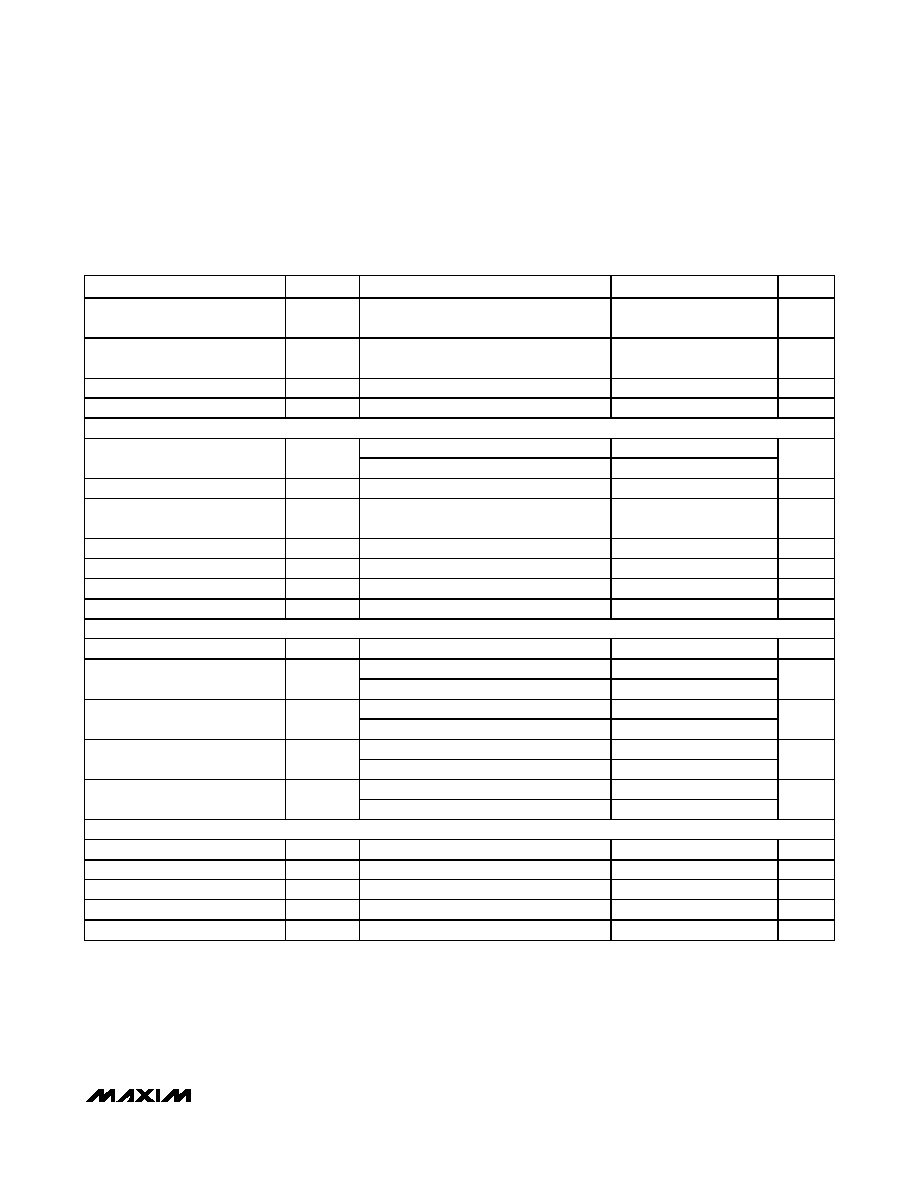
PARAMETER
SYMBOL
CONDITIONS
MIN
TYP
MAX
UNITS
STATIC PERFORMANCE
Resolution
12
Bits
Differential Nonlinearity
DNL
±0.5
LSB
Integral Nonlinearity
INL
±1
LSB
Offset Error
OS
-0.01
±0.003
+0.01
%FS
Offset Drift
±0.03
ppm/∞C
Full-Scale Gain Error
GE
FS
-4
±0.6
+4
%FS
Gain-Error Drift
±110
ppm/∞C
Full-Scale Output Current
I
OUTFS
2
20
mA
Output Compliance
-0.5
+1.1
V
Output Resistance
R
OUT
1
M
Output Capacitance
C
OUT
5
pF
DYNAMIC PERFORMANCE
Maximum Clock Frequency
f
CLK
500
MHz
Minimum Clock Frequency
f
CLK
1
MHz
Maximum DAC Update Rate
f
DAC
f
DAC
= f
CLK
or f
DAC
= f
CLK
/ 2
500
Msps
Minimum DAC Update Rate
f
DAC
f
DAC
= f
CLK
or f
DAC
= f
CLK
/ 2
1
Msps
Maximum Input Data Rate
f
DATA
125
MWps
No interpolation
-151
2x interpolation
-147
f
DATACLK
= 125MHz,
f
OUT
= 16MHz, f
OFFSET
= 10MHz, -12dBFS
4x interpolation
-148
Noise Spectral Density
f
DATACLK
= 125MHz,
f
OUT
= 16MHz, f
OFFSET
= 10MHz, 0dBFS
4x interpolation
-145
dBFS/
Hz
Note 1: Thermal resistance based on a multilayer board with 4 x 4 via array in exposed paddle area.
MAX5893
12-Bit, 500Msps Interpolating and Modulating
Dual DAC with CMOS Inputs
_______________________________________________________________________________________
3
ELECTRICAL CHARACTERISTICS (continued)
(DV
DD1.8
= AV
DD1.8
= 1.8V, AV
CLK
= AV
DD3.3
= DV
DD3.3
= 3.3V, modulator off, 2x interpolation, DATACLK input mode, dual-port
mode, 50
double-terminated outputs, external reference at 1.25V, T
A
= -40∞C to +85∞C, unless otherwise noted. Typical values are
at T
A
= +25∞C, unless otherwise noted.) (Note 2)
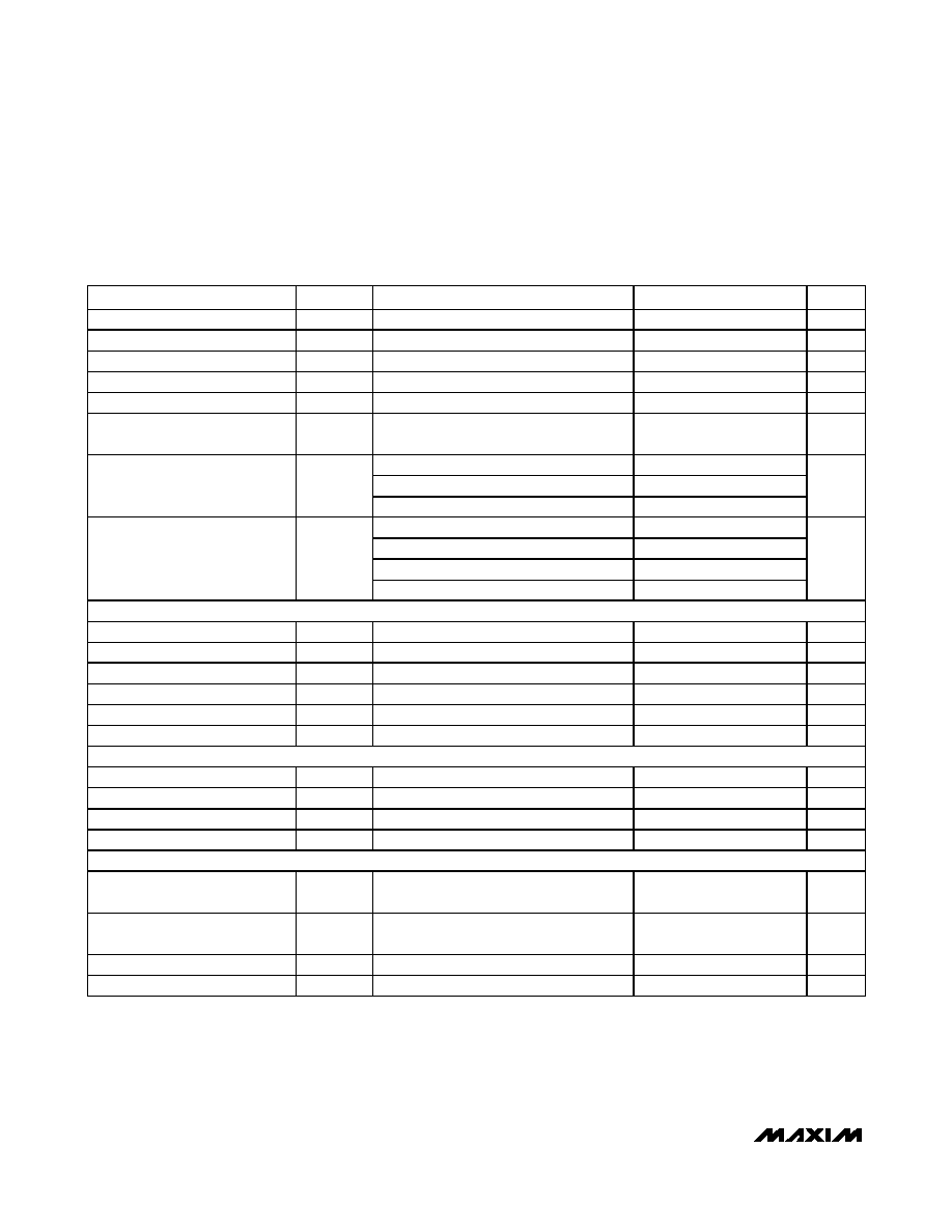
PARAMETER
SYMBOL
CONDITIONS
MIN
TYP
MAX
UNITS
f
OUT
= 10MHz
90
f
OUT
= 30MHz
83
f
DATACLK
= 125MHz,
interpolation off, 0dBFS
f
OUT
= 50MHz
72
f
OUT
= 10MHz
77
88
f
OUT
= 30MHz
83
f
DATACLK
= 125MHz,
2x interpolation, 0dBFS
f
OUT
= 50MHz
84
f
OUT
= 10MHz
90
f
OUT
= 30MHz
84
In-Band SFDR
(DC to f
DATA
/ 2)
SFDR
f
DATACLK
= 125MHz,
4x interpolation, 0dBFS
f
OUT
= 50MHz
86
dBc
No interpolation
-100
2x interpolation
-100
f
DATACLK
= 125MHz,
f
OUT1
= 9MHz, f
OUT2
=
10MHz, -6.1dBFS
4x interpolation
-100
2x interpolation,
f
IM
/ 4 complex
modulation
-73
f
DATA
= 125MHz, f
OUT1
= 79MHz, f
OUT2
=
80MHz, -6.1dBFS
4x interpolation,
f
IM
/ 4 complex
modulation
-75
f
DATACLK
= 62.5MHz,
f
OUT1
= 9MHz, f
OUT2
=
10MHz, -6.1dBFS
8x interpolation
-99
f
DATACLK
= 62.5MHz,
f
OUT1
= 69MHz, f
OUT2
= 70MHz, -6.1dBFS
8x interpolation,
f
IM
/ 4 complex
modulation
-67
Two-Tone IMD
TTIMD
f
DATACLK
= 62.5MHz,
f
OUT1
= 179MHz, f
OUT2
= 180MHz, -6.1dBFS
8x, highpass
interpolation,
f
IM
/ 4 complex
modulation
-62
dBc
Four-Tone IMD
FTIMD
f
DATACLK
= 125MHz, f
OUT
spaced 1MHz
apart from 32MHz, -12dBFS, 2x
interpolation
-93
dBc
4x interpolation
74
f
DATACLK
= 61.44MHz,
f
OUT
= baseband
8x interpolation
73
f
DATACLK
=
122.88MHz, f
OUT
=
61.44MHz
2x interpolation,
f
IM
/ 4 complex
modulation
73
ACLR for WCDMA
(Note 3)
ACLR
f
DATACLK
=
122.88MHz, f
OUT
=
122.88MHz
4x interpolation,
f
IM
/ 4 complex
modulation
69
dB
MAX5893
12-Bit, 500Msps Interpolating and Modulating
Dual DAC with CMOS Inputs
4
_______________________________________________________________________________________
ELECTRICAL CHARACTERISTICS (continued)
(DV
DD1.8
= AV
DD1.8
= 1.8V, AV
CLK
= AV
DD3.3
= DV
DD3.3
= 3.3V, modulator off, 2x interpolation, DATACLK input mode, dual-port
mode, 50
double-terminated outputs, external reference at 1.25V, T
A
= -40∞C to +85∞C, unless otherwise noted. Typical values are
at T
A
= +25∞C, unless otherwise noted.) (Note 2)
PARAMETER
SYMBOL
CONDITIONS
MIN
TYP
MAX
UNITS
Output Propagation Delay
t
PD
1x interpolation (Note 4)
2.9
ns
Output Rise Time
t
RISE
10% to 90% (Note 5)
0.75
ns
Output Fall Time
t
FALL
10% to 90% (Note 5)
1
ns
Output Settling Time
To 0.5% (Note 5)
11
ns
Output Bandwidth
-1dB bandwidth (Note 6)
240
MHz
Passband Width
Ripple <-0.01dB
0.4 x
f
DATA
0.604 x f
DATA
, 2x interpolation
100
0.604 x f
DATA
, 4x interpolation
100
Stopband Rejection
0.604 x f
DATA
, 8x interpolation
100
dB
1x interpolation
22
2x interpolation
70
4x interpolation
146
Data Latency
8x interpolation
311
Clock
Cycles
DAC INTERCHANNEL MATCHING
Gain Match
Gain
f
OUT
= DC - 80MHz, I
OUTFS
= 20mA
±0.1
dB
Gain-Match Tempco
Gain/∞C I
OUTFS
= 20mA
±0.02
ppm/∞C
Phase Match
Phase
f
OUT
= 60MHz, I
OUTFS
= 20mA
±0.13
Deg
Phase-Match Tempco
Phase/∞C f
OUT
= 60MHz, I
OUTFS
= 20mA
±0.006
Deg/∞C
DC Gain Match
I
OUTFS
= 20mA
-0.2
±0.04
+0.2
dB
Channel-to-Channel Crosstalk
f
OUT
= 50MHz, f
DAC
= 250MHz, 0dBFS
-90
dB
REFERENCE
Reference Input Range
0.125
1.250
V
Reference Output Voltage
V
REFIO
Internal reference
1.14
1.20
1.27
V
Reference Input Resistance
R
REFIO
10
k
Reference Voltage Drift
±50
ppm/∞C
CMOS LOGIC INPUT/OUTPUT (A11≠A0, SELIQ/B11, DATACLK/B10, B9≠B0, DATACLK)
Input High Voltage
V
IH
0.7 x
DV
DD1.8
V
Input Low Voltage
V
IL
0.3 x
DV
DD1.8
V
Input Current
I
IN
±1
±20
µA
Input Capacitance
C
IN
3
pF
MAX5893
12-Bit, 500Msps Interpolating and Modulating
Dual DAC with CMOS Inputs
_______________________________________________________________________________________
5
PARAMETER
SYMBOL
CONDITIONS
MIN
TYP
MAX
UNITS
Output High Voltage
V
OH
200µA load
0.8 x
DV
DD3.3
V
Output Low Voltage
V
OL
200µA load
0.2 x
DV
DD3.3
V
Output Leakage Current
Three-state
1
µA
Rise/Fall Time
C
LOAD
= 10pF, 20% to 80%
1.6
ns
CLOCK INPUT (CLKP, CLKN)
Sine-wave input
>1.5
Differential Input Voltage Swing
V
DIFF
Square-wave input
>0.5
V
P-P
Differential Input Slew Rate
>100
V/µs
Common-Mode Voltage
V
COM
AC-coupled
AV
CLK
/
2
V
Input Resistance
R
CLK
5
k
Input Capacitance
C
CLK
3
pF
Minimum Clock Duty Cycle
45
%
Maximum Clock Duty Cycle
55
%
CLKP/CLKN, DATACLK TIMING (Figure 4) (Note 7)
CLK to DATACLK Delay
t
D
DATACLK output mode, C
LOAD
= 10pF
6.2
ns
Capturing rising edge
1.0
Data Hold Time, DATACLK
Input/Output (Pin 14)
t
DH
Capturing falling edge
2.1
ns
Capturing rising edge
0.4
Data Setup Time, DATACLK
Input/Output (Pin 14)
t
DS
Capturing falling edge
-0.7
ns
Capturing rising edge
1.0
Data Hold Time, DATACLK/B10
Input/Output (Pin 27)
t
DH
Capturing falling edge
2.3
ns
Capturing rising edge
0.2
Data Setup Time, DATACLK/B10
Input/Output (Pin 27)
t
DS
Capturing falling edge
-0.4
ns
SERIAL PORT INTERFACE TIMING (Figure 3) (Note 7)
SCLK Frequency
f
SCLK
10
MHz
CS Setup Time
t
SS
2.5
ns
Input Hold Time
t
SDH
0
ns
Input Setup Time
t
SDS
4.5
ns
Data Valid Duration
t
SDV
6.5
16.5
ns
ELECTRICAL CHARACTERISTICS (continued)
(DV
DD1.8
= AV
DD1.8
= 1.8V, AV
CLK
= AV
DD3.3
= DV
DD3.3
= 3.3V, modulator off, 2x interpolation, DATACLK input mode, dual-port
mode, 50
double-terminated outputs, external reference at 1.25V, T
A
= -40∞C to +85∞C, unless otherwise noted. Typical values are
at T
A
= +25∞C, unless otherwise noted.) (Note 2)