 | ÐлекÑÑоннÑй компоненÑ: MAX5902 | СкаÑаÑÑ:  PDF PDF  ZIP ZIP |
Äîêóìåíòàöèÿ è îïèñàíèÿ www.docs.chipfind.ru
MAX5902/MAX5903
+72V SOT23 Simple Swapper Hot-Swap
Controllers
________________________________________________________________ Maxim Integrated Products
1
19-1988; Rev 1; 9/02
General Description
The MAX5902/MAX5903 are SOT23 hot-swap con-
trollers that allow a circuit card to be safely hot plugged
into a live backplane without causing a glitch on the
power-supply rail. These devices operate from +9V to
+72V and provide the simplest hot-swap solution by
eliminating all external components except the external
P-channel MOSFET.
The MAX5902/MAX5903 limit the inrush current to the
load and provide a circuit breaker function for overcur-
rent protection. During startup the circuit breaker func-
tion is disabled and the MAX5902/MAX5903 limit the
inrush current by gradually turning on the external
MOSFET. Once the external MOSFET is fully enhanced,
the circuit breaker function is enabled and the
MAX5902/MAX5903 provide overcurrent protection by
monitoring the voltage drop across the external MOS-
FET's on-resistance.
The MAX5902/MAX5903 include an undervoltage lock-
out (UVLO) function, ON/OFF control input and a
power-good status output, PGOOD (MAX5902) or
PGOOD (MAX5903). A built in thermal shutdown fea-
ture is also included to protect the external MOSFET in
case of overheating.
The MAX5902/MAX5903 offer latched or auto-retry fault
management and are available with 300mV, 400mV or
500mV circuit breaker thresholds. Both the MAX5902
and MAX5903 are available in a small SOT23 package,
and are specified for the extended -40°C to +85°C tem-
perature range. For specific ordering information refer
to the selector guide at the end of the data sheet.
Applications
Network Routers
Servers
Network Switches
RAID
Base Station Line
Industrial Systems
Cards
Features
o Wide +9V to +72V Operation
o Requires No External Sense Resistor
o Drives External P-Channel MOSFET
o Limits Inrush Current
o Circuit Breaker Function
o Less than 2mA Quiescent Current
o ON/OFF Input Permits Load Power-Supply
Control and Sequencing
o Adjustable Undervoltage Lockout
o Power-Good Output with +72V Rating
o Latching or Automatic Retry Fault Management
o Thermal Shutdown Helps Protect the External
MOSFET
o Space-Saving SOT23-6 Package
Ordering Information
PART
TEMP RANGE
PIN-PACKAGE
MAX5902_ _EUT*
-40
°C to +85°C
6-SOT23
MAX5903_ _EUT*
-40
°C to +85°C
6-SOT23
*For specific part numbers see Selector Guide at end of data
sheet.
GND
1
6
ON/OFF
5
PGOOD (PGOOD)
V
S
MAX5902
MAX5903
SOT23-6
TOP VIEW
( ) ARE FOR MAX5903 ONLY.
2
3
4
DRAIN
GATE
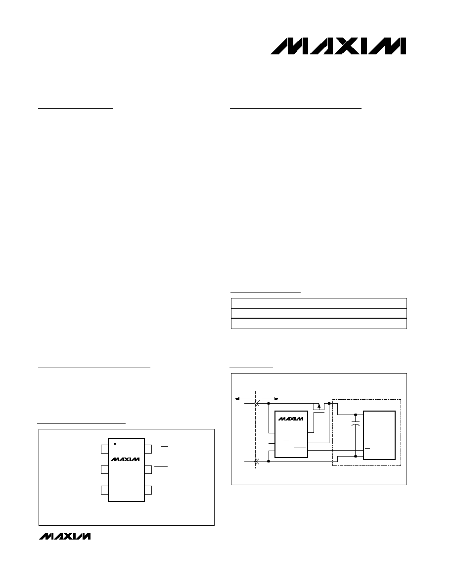
Pin Configuration
Typical Operating Circuits
GND
ON/OFF
HOT-SWAP CONTROLLER
V
S
GND
50W ISOLATED
POWER SUPPLY
V
IN
(-)
ON/OFF
LUCENT
JW050A1
V
IN
(+)
GATE
DRAIN
PGOOD
+48V
BACKPLANE
CIRCUIT CARD
IRFR5410
MAX5902
Typical Operating Circuits continued at end of data sheet.
Simple Swapper is a trademark of Maxim Integrated Products Inc.
For pricing, delivery, and ordering information, please contact Maxim/Dallas Direct! at
1-888-629-4642, or visit Maxim's website at www.maxim-ic.com.
MAX5902/MAX5903
+72V SOT23 Simple Swapper Hot-Swap
Controllers
2
_______________________________________________________________________________________
ABSOLUTE MAXIMUM RATINGS
ELECTRICAL CHARACTERISTICS
(V
S
= +9V to +72V, GND = 0, ON/OFF open circuit, T
A
= -40
°C to +85°C, unless otherwise noted. Typical values are at V
S
= +48V
and T
A
= +25
°C.) (Notes 2, 3)
Stresses beyond those listed under "Absolute Maximum Ratings" may cause permanent damage to the device. These are stress ratings only, and functional
operation of the device at these or any other conditions beyond those indicated in the operational sections of the specifications is not implied. Exposure to
absolute maximum rating conditions for extended periods may affect device reliability.
Terminal Voltage (with respect to GND unless otherwise noted)
V
S
, DRAIN, PGOOD, PGOOD ................................-0.3V to +76V
ON/OFF ....................................................................-0.3V to +4V
GATE to V
S
............................................................-12V to +0.3V
Current into any Pin ............................................................±3mA
Continuous Power Dissipation at T
A
= +70
°C
6-Pin SOT23 (derate 9.1mW/
°C above +70°C)..........727mW
Maximum Junction Temperature .....................................+150
°C
Storage Temperature Range .............................-60
°C to +150°C
Lead Temperature .............................................................Note 1
PARAMETER
SYM B O L C
O ND IT IO N S
M IN
T YP
M A X
U N IT S
Supply Voltage
V
S
9
72
V
Supply Current
I
GND
M easur ed out of G N D , P GO O D or PGOOD
op en ci r cui t, D RAIN = V
S
1
2
mA
V
S
= +36V to +72V
9
10
11
External Gate Drive
V
GS
V
S
- V
GATE
V
S
= +9V
8
8.5
V
V
S
= +36V to +72V
5
9
18
Load Voltage Slew Rate
Magnitude
SR
| dV
DRAIN
/dt |
C
L
= 10µF
V
S
= +9V
3
6
11
V/ms
Default Undervoltage Lockout
V
UVLO
V
S
increasing
28.5
31.5
34.5
V
Undervoltage Lockout
Hysteresis
3.5
V
ON/OFF Pin Input Resistance
R
ON/OFF
19
32
52
k
DRAIN to GND Resistance
R
DGND
900
k
DRAIN to V
S
Resistance
R
DS
650
k
ON/OFF Reference Threshold
V
ON/OFF
V
ON/OFF
Increasing
1.14
1.26
1.38
V
ON/OFF Hysteresis
140
mV
Start Delay (Note 4)
t
ON
80
150
280
ms
ON/OFF Off Delay (Note 5)
t
OFF
V
S
- V
GATE
< 1V
5
10
18
ms
MAX590_ _AEUT
200
300
460
MAX590_ _BEUT
280
400
540
Circuit Breaker Threshold
V
CB
V
S
- V
DRAIN
MAX590_ _CEUT
400
500
660
mV
C
GATE
= 1nF
2
6.5
C
GATE
= 4.7nF
4
11
Circuit Breaker Delay (Note 6)
t
CB
(V
S
- V
DRAIN
) > V
CB
until (V
S
- V
GATE
)
< 1V, 200mV
overdrive step
C
GATE
= 10nF
7
17
µs
Restart Delay (Note 4)
t
RS
After circuit breaker event,
MAX590_ A_EUT only
80
150
280
ms
P ow er G ood O utp ut Low V ol tag e
V
OL
I
OL
= 1mA
0.3
0.6
V
Note 1: This device is constructed using a unique set of packaging techniques that impose a limit on the thermal profile the device
can be exposed to during board level solder attach and rework. This limit permits only the use of solder profiles recom-
mended in the industry standard specification, JEDEC 020A, paragraph 7.6, Table 3 for IR/VPR and convection reflow.
Preheating is required. Hand or wave soldering is not allowed.
MAX5902/MAX5903
+72V SOT23 Simple Swapper Hot-Swap
Controllers
_______________________________________________________________________________________
3
Note 2: All currents into device pins are positive, all currents out of device pins are negative, and all voltages are referenced to
GND, unless otherwise noted.
Note 3: All specifications are 100% tested at T
A
= +25°C, unless otherwise noted. Specifications over -40°C to +85°C are guaran-
teed by characterization.
Note 4: This is the delay time from a valid on condition until V
GS
begins rising. Valid on conditions are: the device is not in undervolt-
age lockout; ON/OFF is not driven low; and the device is not in thermal shutdown.
Note 5: This is the delay from a valid low on ON/OFF until V
GS
falls. Pulses on ON/OFF less than t
OFF
are ignored, offering glitch
immunity.
Note 6: Guaranteed by characterization, not production tested. C
GATE
is a capacitor from GATE to V
S
.
ELECTRICAL CHARACTERISTICS (continued)
(V
S
= +9V to +72V, GND = 0, ON/OFF open circuit, T
A
= -40
°C to +85°C, unless otherwise noted. Typical values are at V
S
= +48V
and T
A
= +25
°C.) (Notes 2, 3)
PARAMETER
SYM B O L C
O ND IT IO N S
M IN
T YP
M A X
U N IT S
Power-Good Output Open-Drain
Leakage Current
I
OH
V
PGOOD
= 72V (MAX5902)
V
PGOOD
= 72V (MAX5903)
10
µA
Thermal Shutdown Temperature
T
SD
Junction temperature
+125
°C
Thermal Shutdown Hysteresis
T
HY
15
°C
Typical Operating Characteristics
(V
S
= +48V, GND = 0, and T
A
= +25
°C, unless otherwise noted. See Figure 2 for test circuits.)
0.7
0.8
1.0
0.9
1.1
1.2
0
30
15
45
60
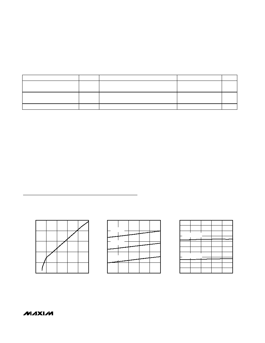
75
SUPPLY CURRENT
vs. INPUT VOLTAGE
MAX5902 toc01
INPUT VOLTAGE (V)
SUPPLY CURRENT (mA)
0.7
0.8
1.0
0.9
1.1
1.2
-40
10
-15
35
60
85
SUPPLY CURRENT
vs. TEMPERATURE
MAX5902 toc02
TEMPERATURE (
°C)
SUPPLY CURRENT (mA)
V
IN
= +70V
V
IN
= +48V
V
IN
= +12V
25
28
27
26
29
30
31
32
33
34
35
-40
10
-15
35
60
85
V
UVLO
THRESHOLD
vs. TEMPERATURE
MAX5902 toc03
TEMPERATURE (
°C)
LOCKOUT VOLTAGE (V)
INCREASING V
IN
DECREASING V
IN
t = 1µs/div
CIRCUIT BREAKER EVENT
V
OVERDRIVE
= 20mV, C
GATE
= 1000pF
A
B
C
MAX5902 toc10
0
0
0
A : V
DS
, 0.5V/div
B : V
GS
, 10V/div
C : V
PGOOD
TO V
S
, 50V/div
t = 1µs/div
CIRCUIT BREAKER EVENT
V
OVERDRIVE
= 200mV, C
GATE
= 1000pF
A
B
C
MAX5902 toc11
0
0
0
A : V
DS
, 0.5V/div
B : V
GS
, 10V/div
C : V
PGOOD
TO V
S
, 50V/div
Typical Operating Characteristics (continued)
(V
S
= +48V, GND = 0, and T
A
= +25
°C, unless otherwise noted. See Figure 2 for test circuits.)
MAX5902/MAX5903
+72V SOT23 Simple Swapper Hot-Swap
Controllers
4
_______________________________________________________________________________________
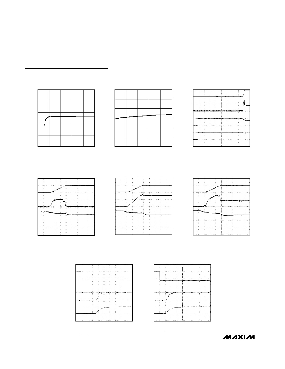
5
7
11
9
13
15
0
30
15
45
60
75
GATE DRIVE VOLTAGE
vs. INPUT VOLTAGE
MAX5902 toc04
INPUT VOLTAGE (V)
GATE DRIVE (V)
75
125
100
175
150
200
225
-40
10
-15
35
60
85
RETRY TIMEOUT
vs. TEMPERATURE
MAX5902 toc05
TEMPERATURE (
°C)
TIMEOUT PERIOD (ms)
t = 20ms/div
TURN-ON WAVEFORMS
R
L
= 60
, C
L
= 100
µF
A : V
OUT
, 50V/div
B : I
IN
, 1A/div
C : V
GATE
, 50V/div
D : V
IN
, 50V/div
A
B
D
C
MAX5902 toc06
0
0
0
0
t = 2ms/div
TURN-ON WAVEFORMS
R
L
= OPEN, C
L
= 100
µF
A : V
OUT
, 50V/div
B : I
IN
, 1A/div
C : V
GATE
, 20V/div
A
B
C
MAX5902 toc07
0
0
0
t = 2ms/div
TURN-ON WAVEFORMS
R
L
= 60
, C
L
= 10
µF
A : V
OUT
, 50V/div
B : I
IN
, 0.5A/div
C : V
GATE
, 20V/div
A
B
C
MAX5902 toc08
0
0
0
t = 2ms/div
TURN-ON WAVEFORMS
R
L
= 60
, C
L
= 100
µF
A : V
OUT
, 50V/div
B : I
IN
, 1A/div
C : V
GATE
, 20V/div
A
B
C
MAX5902 toc09
0
0
0
MAX5902/MAX5903
+72V SOT23 Simple Swapper Hot-Swap
Controllers
_______________________________________________________________________________________
5
Detailed Description
The MAX5902/MAX5903 are integrated hot-swap con-
troller ICs contained in 6-pin SOT23 packages. They
allow a board to be safely hot-plugged into a live back-
plane without causing a glitch on the power-supply rail.
They are well suited for +48V power systems allowing
cost-effective, simple, and compact design. The
MAX5902/MAX5903 operate from +9V to +72V to cover
a wide range of end equipment hot-swap needs. They
require only an external P-channel power MOSFET to
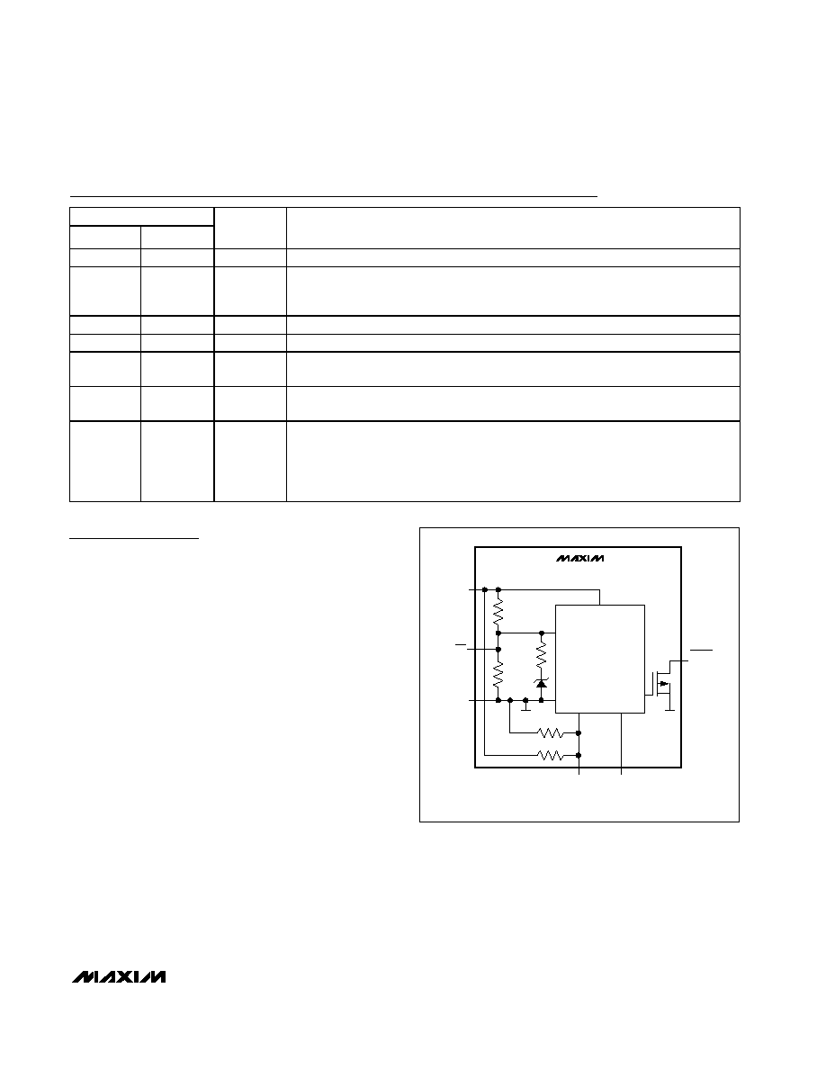
provide hot-swap control. Figure 1 shows a functional
block diagram of the MAX5902/MAX5903.
The MAX5902/MAX5903 controls an external P-channel
power MOSFET placed in the positive power-supply
pathway. When power is first applied, the MAX5902/
MAX5903 keep the MOSFET turned off. The
MAX5902/MAX5903 hold the MOSFET off indefinitely if
ON/OFF is held low, if the supply voltage is below the
undervoltage lockout level, or if the die temperature
exceeds +125°C. If none of these conditions exist for
150ms (typ), the MAX5902/MAX5903 begin to gradually
turn on the MOSFET. During this turn-on phase, the
MAX5902/MAX5903 slowly enhance the MOSFET,
allowing the voltage on the load, i.e. the drain of the
MOSFET, to rise at a rate of 9V/ms (typ). The inrush cur-
rent to the load is thus limited to a level proportional to
the load capacitance, and the constant slew rate. After
the MOSFET is fully enhanced, and the load voltage is
settled to its final value, the MAX5902A/ MAX5903A and
MAX5902L/MAX5903L monitor the voltage drop across
the MOSFET. If the voltage drop exceeds the circuit
breaker threshold the MAX5902A/MAX5903A and
MAX5902L/MAX5903L turn off the MOSFET, discon-
V
S
ON/OFF
GND
GND
GND
3V
MAX5902
MAX5903
828k
*900k
34.5k
1k
GATE
DRAIN
CONTROL
LOGIC
PGOOD
(PGOOD)
( ) ARE FOR THE MAX5903 ONLY
* RELATIVE TOLERANCE
±1%, ABSOLUTE TOLERANCE ±50% (TYP)
*650k
*
*
Figure 1. Functional Block Diagram
Pin Description
PIN
MAX5902
MAX5903
NAME
FUNCTION
1
1
V
S
Positive Supply Voltage Input and External P-Channel MOSFET Source Connection
2
2
DRAIN
Drain Sense Input for External P-Channel MOSFET. Connect DRAIN as close as
possible to the MOSFET's drain and use wide circuit traces to assure good thermal
coupling between the MAX5902/MAX5903 and the MOSFET. See Layout Guidelines.
3
3
GATE
Gate Drive Output for External P-Channel MOSFET
4
4
GND
Ground Connection
5
--
PGOOD
Power Good Output. PGOOD is an N-channel, open-drain, active-low output,
referenced to GND.
--
5
PGOOD
Power Good Output. PGOOD is an N-channel, open-drain, active-high output,
referenced to GND.
6
6
ON/OFF
ON/OFF Control Input. ON/OFF is referenced to GND. Drive ON/OFF above 1.38V or
leave unconnected to enable the device. Drive ON/OFF below 1V to disable the device.
ON/OFF is also used to adjust the UVLO threshold. Internally clamped to nominally 3V
through a 1k
resistor. (See Figure 1.) (See Undervoltage Lockout in the Applications
section of this data sheet.)