 | ÐлекÑÑоннÑй компоненÑ: MAX5904 | СкаÑаÑÑ:  PDF PDF  ZIP ZIP |
Äîêóìåíòàöèÿ è îïèñàíèÿ www.docs.chipfind.ru
General Description
The MAX5904MAX5909 dual hot-swap controllers
provide complete protection for dual-supply systems.
These devices hot swap two supplies ranging from +1V
to +13.2V, provided one supply is at or above 2.7V,
allowing the safe insertion and removal of circuit cards
into live backplanes.
The discharged filter capacitors of the circuit card pro-
vide low impedance to the live backplane. High inrush
currents from the backplane to the circuit card can burn
up connectors and components, or momentarily col-
lapse the backplane power supply leading to a system
reset. The MAX5904 family of hot-swap controllers pre-
vents such problems by gradually ramping up the output
voltage and regulating the current to a preset limit when
the board is plugged in, allowing the system to stabilize
safely. After the startup cycle is completed, two on-chip
comparators provide VariableSpeed/BiLevelTM protec-
tion against short-circuit and overcurrent faults, as well
as immunity against system noise and load transients. In
the event of a fault condition, the load is disconnected.
The MAX5905/MAX5907/MAX5909 must be unlatched
after a fault, and the MAX5904/MAX5906/MAX5908 auto-
matically restart after a fault.
The MAX5904 family offers a variety of options to reduce
component count and design time. All devices integrate
an on-board charge pump to drive the gates of low-cost,
external N-channel MOSFETs. The devices offer integrat-
ed features like startup current regulation and current
glitch protection to eliminate external timing resistors and
capacitors. The MAX5906MAX5909 provide an open-
drain status output, an adjustable startup timer, an
adjustable current limit, an uncommitted comparator,
and output undervoltage/overvoltage monitoring.
The MAX5904/MAX5905 are available in 8-pin SO pack-
ages. The MAX5906MAX5909 are available in space-
saving 16-pin QSOP packages.
Applications
PCI-Express Applications
Basestation Line Cards
Network Switches or Routers
Solid-State Circuit Breaker
Power-Supply Sequencing
Hot Plug-In Daughter Cards
RAID
Features
o Safe Hot Swap for +1V to +13.2V Power
Supplies
Requires One Input
2.7V
o Low 25mV Default Current-Limit Threshold
o Inrush Current Regulated at Startup
o Circuit Breaker Function
o Adjustable Circuit Breaker/Current-Limit
Threshold
o VariableSpeed/BiLevel Circuit-Breaker Response
o Auto-Retry or Latched Fault Management
o On/Off Sequence Programming
o Status Output Indicates Fault/Safe Condition
o Output Undervoltage and Overvoltage Monitoring
and/or Protection
MAX5904MAX5909
Low-Voltage, Dual Hot-Swap Controllers/Power
Sequencers
________________________________________________________________ Maxim Integrated Products
1
GATE2
ON
GND
1
2
8
7
IN2
SENSE2
SENSE1
GATE1
IN1
NARROW SO
TOP VIEW
3
4
6
5
MAX5904
MAX5905
Pin Configurations
Ordering Information
19-2238; Rev 2; 11/03
EVALUATION KIT
AVAILABLE
For pricing, delivery, and ordering information, please contact Maxim/Dallas Direct! at
1-888-629-4642, or visit Maxim's website at www.maxim-ic.com.
PART
TEMP RANGE
PIN-PACKAGE
MAX5904ESA*
-40
°C to +85°C
8 SO
MAX5904USA
0
°C to +85°C
8 SO
MAX5905ESA*
-40
°C to +85°C
8 SO
MAX5905USA
0
°C to +85°C
8 SO
MAX5906EEE*
-40
°C to +85°C
16 QSOP
MAX5906UEE
0
°C to +85°C
16 QSOP
MAX5907EEE*
-40
°C to +85°C
16 QSOP
MAX5907UEE
0
°C to +85°C
16 QSOP
MAX5908EEE*
-40
°C to +85°C
16 QSOP
MAX5908UEE
0
°C to +85°C
16 QSOP
MAX5909EEE*
-40
°C to +85°C
16 QSOP
MAX5909UEE
0
°C to +85°C
16 QSOP
Selector Guide and Typical Operating Circuits appear at end
of data sheet.
VariableSpeed/BiLevel is a trademark of Maxim Integrated
Products, Inc.
Pin Configurations continued at end of data sheet.
*Contact factory for availability.
MAX5904MAX5909
Low-Voltage, Dual Hot-Swap Controllers/Power
Sequencers
2
_______________________________________________________________________________________
ABSOLUTE MAXIMUM RATINGS
ELECTRICAL CHARACTERISTICS
(V
IN
_ = +1V to +13.2V provided at least one supply is higher than +2.7V, V
ON
= +2.7V, T
A
= T
MIN
to T
MAX
, unless otherwise noted.
Typical values are at V
IN1
= +5V, V
IN2
= +3.3V, and T
A
= +25°C.) (Note 1)
Stresses beyond those listed under "Absolute Maximum Ratings" may cause permanent damage to the device. These are stress ratings only, and functional
operation of the device at these or any other conditions beyond those indicated in the operational sections of the specifications is not implied. Exposure to
absolute maximum rating conditions for extended periods may affect device reliability.
IN_ to GND...........................................................................+14V
GATE_ to GND..........................................+0.3V to (V
IN
_ + 6.2V)
ON, PGOOD, COMP+, COMPOUT, TIM to GND.......-0.3V to the
higher of (V
IN1
+ 0.3V) and (V
IN2
+ 0.3V)
SENSE_, MON_, LIM_ to GND ...................-0.3V to (V
IN
_ + 0.3V)
Current into Any Pin .........................................................±50mA
Continuous Power Dissipation (T
A
= +70°C)
8-Pin Narrow SO (derate 5.9mW/°C above +70°C) ......471mW
16-Pin QSOP (derate 8.3mW/°C above +70°C)............667mW
Operating Temperature Ranges:
MAX590_U_ _ .....................................................0°C to +85°C
MAX590_E_ _ ...................................................-40°C to +85°C
Storage Temperature Range .............................-65°C to +150°C
PARAMETER
SYMBOL
CONDITIONS
MIN
TYP
MAX
UNITS
POWER SUPPLIES
IN_ Input Voltage Range
V
IN
_
Other V
IN
= +2.7V
1.0
13.2
V
Supply Current
I
IN
I
IN1
+ I
IN2
1.2
2.3
mA
CURRENT CONTROL
T
A
= +25°C
22.5
25
27.5
MAX5904/MAX5905
T
A
= T
MIN
to T
MAX
20.5
27.5
LIM = GND
22.5
25
27.5
Slow-Comparator Threshold
(V
IN
- V
SENSE
) (Note 2)
V
SC,TH
MAX5906MAX5909
R
LIM
= 300k
80
100
125
mV
1mV overdrive
3
ms
Slow-Comparator Response Time
(Note 3)
t
SCD
50mV overdrive
110
µs
V
SU,TH
V
IN
_ - V
SENSE
_; during startup
2 x V
SC, TH
Fast-Comparator Threshold
V
FC,TH
V
IN
_ - V
SENSE
_; normal operation
4 x V
SC, TH
mV
Fast-Comparator Response Time
t
FCD
10mV overdrive, from overload condition
260
ns
SENSE Input Bias Current
I
B SEN
V
SEN
_ = V
IN
_
0.03
6
µA
MOSFET DRIVER
R
TIM
= 100k
8
10.8
13.6
R
TIM
= 4k
(minimum value)
0.35
0.45
0.55
Startup Period
(Note 4)
t
START
TIM floating for MAX5906MAX5909
fixed for MAX5904/MAX5905
5
9
14
ms
Charging, V
GATE
= +5V, V
IN
= +10V
(Note 5)
80
100
130
µA
Weak discharge, during startup when current
limit is active or when 0.4V < V
ON
< 0.8V
100
µA
Average Gate Current
I
GATE
Strong discharge, triggered by a fault or
when V
ON
< 0.4V
3
mA
Gate Drive Voltage
V
DRIVE
V
GATE
_ - V
IN
_, I
GATE
_ < 1µA
4.8
5.4
5.8
V
ON COMPARATOR
Low to high
0.375
0.4
0.425
V
Fast Pulldown ON Threshold
V
ONFP,TH
Hysteresis
25
mV
MAX5904MAX5909
Low-Voltage, Dual Hot-Swap Controllers/Power
Sequencers
_______________________________________________________________________________________
3
Note 1: Limits are 100% tested at T
A
= +25°C and +85°C. Limits at 0°C and -40° are guaranteed by characterization and are not produc-
tion tested.
Note 2 The MAX5906MAX5909 slow-comparator threshold is adjustable. V
SC,TH
= R
LIM
x 0.25µA + 25mV (see Typical Operating
Characteristics).
Note 3: The current-limit slow-comparator response time is weighted against the amount of overcurrent; the higher the overcurrent
condition, the faster the response time. See Typical Operating Characteristics.
Note 4: The startup period (t
START
) is the time during which the slow comparator is ignored and the device acts as a current limiter
by regulating the sense current with the fast comparator. See the Startup Period section.
ELECTRICAL CHARACTERISTICS (continued)
(V
IN
_ = +1V to +13.2V provided at least one supply is higher than +2.7V, V
ON
= +2.7V, T
A
= T
MIN
to T
MAX
, unless otherwise noted.
Typical values are at V
IN1
= +5V, V
IN2
= +3.3V, and T
A
= +25°C.) (Note 1)
PARAMETER
SYMBOL
CONDITIONS
MIN
TYP
MAX
UNITS
Low to high
0.80
0.825
0.85
V
Channel 1 ON Threshold
V
ON1,TH
Hysteresis
25
mV
Low to high
1.95
2.025
2.07
V
Channel 2 ON Threshold
V
ON2,TH
Hysteresis
25
mV
ON Propagation Delay
t
ON
10mV overdrive
50
µs
V
ON
< 4.5V
0.03
V
ON
> 4.5V
100
ON Input Bias Current
I
BON
V
IN1
= V
IN2
= +13.2V
V
ON
= 4V
0.03
1
µA
ON Pulse Width Low
t
UNLATCH
To unlatch after a latched fault
100
µs
DIGITAL OUTPUT (PGOOD)
Output Leakage Current
V
PGOOD
= 13.2V
1
µA
Output Voltage Low
V
OL
I
SINK
= 1mA
0.4
V
PGOOD Delay
t
PGDLY
After t
START
, MON_ = V
IN_
0.75
ms
OUTPUT VOLTAGE MONITORS (MON1, MON2)
Overvoltage
657
687
707
MON_ Trip Threshold
V
MON
_
Undervoltage
513
543
563
mV
MON_ Glitch Filter
20
µs
MON_ Input Bias Current
V
MON
_ = 600mV
0.03
µA
UNDERVOLTAGE LOCKOUT (UVLO)
S tar tup i s i ni ti ated w hen thi s thr eshol d i s r eached
b y V
IN 1
or V
IN 2
, V
ON
> 0.8V , V
IN_
i ncr easi ng
2.1
2.4
2.67
V
UVLO Threshold
V
UVLO
Hysteresis
100
mV
UVLO Glitch Filter Reset Time
V
IN
_ = 0V, to unlatch after a fault
100
µs
UVLO to Startup Delay
t
D,UVLO
V
IN_
step from 0 to 2.8V
20
37.5
60
ms
SHUTDOWN RESTART
Auto-Retry Delay
t
RETRY
Delay time to restart after a fault shutdown
MAX5904/MAX5906/MAX5908
64 x t
START
ms
UNCOMMITTED COMPARATOR
Low to high
1.206
1.236
1.266
V
INC+ Trip Threshold Voltage
V
C,TH
Hysteresis
10
mV
Propagation Delay
10mV overdrive
50
µs
OUTC Voltage Low
V
OL
I
SINK
= 1mA
0.4
V
INC+ Bias Current
V
INC+
= 5V
0.02
1
µA
OUTC Leakage Current
I
OUTC
V
OUTC
=
13.2V
0.02
1
µA
MAX5904MAX5909
Low-Voltage, Dual Hot-Swap Controllers/Power
Sequencers
4
_______________________________________________________________________________________
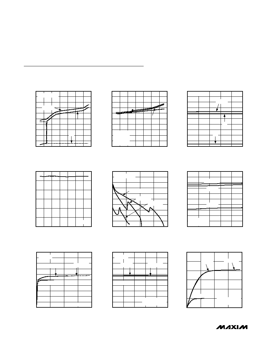
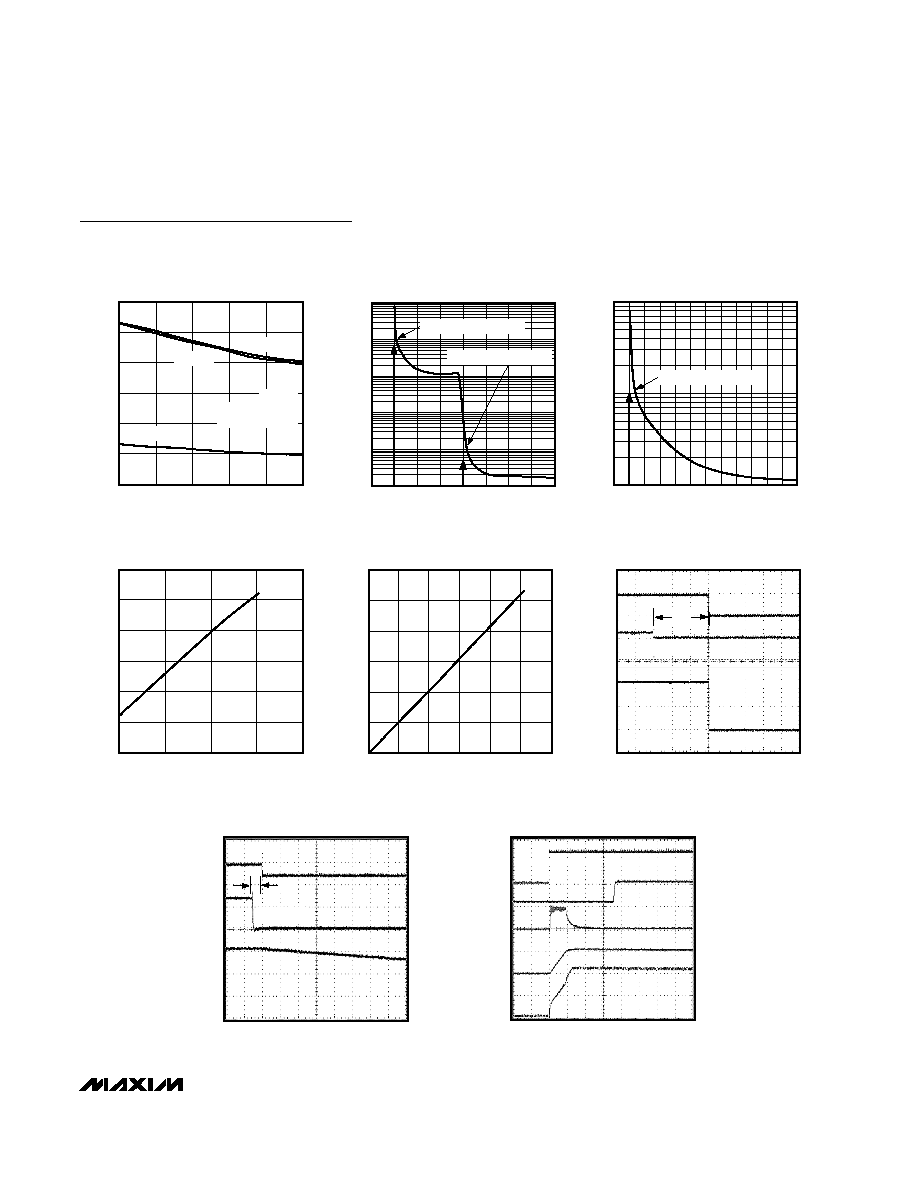
Typical Operating Characteristics
(Typical Operating Circuits, Q1 = Q2 = Fairchild FDB7090L, V
IN1
= +5V, V
IN2
= +3.3V, T
A
= +25°C, unless otherwise noted. Channels
1 and 2 are identical in performance. Where characteristics are interchangeable, channels 1 and 2 are referred to as X and Y.)
0
0.6
0.4
0.2
1.0
0.8
1.8
1.6
1.4
1.2
2.0
0
2
4
6
8
10
12
14
SUPPLY CURRENT
vs. SUPPLY VOLTAGE
MAX5904 toc01
V
INX
(V)
I
IN
(mA)
V
INY
= V
ON
= 2.7V
I
INX
+ I
INY
I
INX
I
INY
0
0.6
0.4
0.2
1.0
0.8
1.8
1.6
1.4
1.2
2.0
0
2
4
6
8
10
12
14
TOTAL SUPPLY CURRENT
vs. SUPPLY VOLTAGE
MAX5904 toc02
V
INX
(V)
I
IN
(mA)
V
INY
= 5.0V
A) V
ON
= 3.3V
B) V
ON
= 1.5V
C) V
ON
= 0V
A
C
B
0
0.6
0.4
0.2
0.8
1.0
1.2
1.4
1.6
1.8
2.0
-40
10
-15
35
60
85
SUPPLY CURRENT
vs. TEMPERATURE
MAX5904 toc03
TEMPERATURE (
°C)
I
IN
(mA)
V
ON
= V
IN1
I
IN1
+ I
IN2
I
IN2
I
IN1
0
2
1
4
3
5
6
0
6
8
2
4
10
12
14
GATE DRIVE VOLTAGE vs.
INPUT VOLTAGE
MAX5904 toc04
V
INX
(V)
GATE DRIVE VOLTAGE (V)
V
INY
= 2.7V
0
60
40
20
80
100
120
140
160
180
200
0
20
GATE CHARGE CURRENT
vs. GATE VOLTAGE
MAX5904 toc05
V
GATEX
(V)
GATE CHARGE CURRENT (
µ
A)
5
10
15
V
ON
= V
INY
= 2.7V
V
INX
= 13.2V
V
INX
= 5V
V
INX
= 1V
0
60
40
20
80
100
120
140
160
180
200
-40
10
-15
35
60
85
GATE CHARGE CURRENT
vs. TEMPERATURE
MAX5904 toc06
TEMPERATURE (
°C)
GATE CHARGE CURRENT (
µ
A)
V
INX
= 13.2V
V
INX
= 5V
V
INX
= 1V
V
ON
= V
INY
= 2.7V
V
GATEX
= 0V
0
60
40
20
80
100
120
140
160
180
200
0
5
15
10
20
GATE WEAK DISCHARGE CURRENT
vs. GATE VOLTAGE
MAX5904 toc07
V
GATEX
(V)
GATE DISCHARGE CURRENT (
µ
A)
V
ON
= 0.6V
V
INY
= 2.7V
V
INX
= 13.2V
V
INX
= 5V
V
INX
= 1V
0
60
40
20
80
100
120
140
160
180
200
-40
-15
35
60
10
85
GATE WEAK DISCHARGE CURRENT
vs. TEMPERATURE
MAX5904 toc08
TEMPERATURE (
°C)
GATE DISCHARGE CURRENT (
µ
A)
V
ON
= 0.6V
V
INX
= 13.2V
V
INX
= 5V
V
INX
= 1V
V
INY
= 2.7V
V
GATEX
= V
INX
+ 6.2V
0
2
1
4
3
5
6
0
10
5
15
20
GATE STRONG DISCHARGE CURRENT
vs. GATE VOLTAGE
MAX5904 toc09
V
GATEX
(V)
GATE DISCHARGE CURRENT (mA)
V
INX
= 13.2V
V
INX
= 5V
V
INX
= 1V
V
ON
= 0V
V
INY
= 2.7V
V
GATEX
= V
INX
+ 6.2V
MAX5904MAX5909
Low-Voltage, Dual Hot-Swap Controllers/Power
Sequencers
_______________________________________________________________________________________
5
0
2
1
4
3
5
6
-40
10
-15
35
60
85
GATE STRONG DISCHARGE CURRENT
vs. TEMPERATURE
MAX5904 toc10
TEMPERATURE (
°C)
GATE DISCHARGE CURRENT (mA)
V
INX
= 13.2V
V
INX
= 5V
V
INX
= 1V
V
ON
= 0V
V
INY
= 2.7V
V
GATEX
= V
INX
+ 6.2V
0.0001
0.001
0.1
0.01
1
10
0
50
75
25
100 125 150 175 200
TURN-OFF TIME vs. SENSE VOLTAGE
MAX5904 toc11
V
IN
- V
SENSE
(mV)
TURN-OFF TIME (ms)
SLOW-COMP. THRESHOLD
FAST-COMP. THRESHOLD
0.1
1
10
20
30 35
25
40 45 50 55 60 65 70 75 80
TURN-OFF TIME vs. SENSE VOLTAGE
(EXPANDED SCALE)
MAX5904 toc12
V
IN
- V
SENSE
(mV)
TURN-OFF TIME (ms)
SLOW-COMP. THRESHOLD
0
40
20
80
60
100
120
0
200
100
300
400
SLOW-COMPARATOR THRESHOLD
vs. R
LIM
MAX5904 toc13
R
LIM
(k
)
V
SC, TH
(mV)
0
20
10
40
30
50
60
STARTUP PERIOD vs. R
TIM
MAX5904 toc14
R
TIM
(k
)
t
START
(ms)
0
200
300
100
400
500
600
0V
0V
0V
V
PGOOD
5V/div
V
SENSE
- V
IN
100mV/div
V
GATE
5V/div
TURN-OFF TIME
SLOW-COMPARATOR FAULT
MAX5904 toc15
1ms/div
V
IN
= 5.0V
t
SCD
26mV STEP
0V
0V
0V
V
PGOOD
5V/div
V
SENSE
- V
IN
100mV/div
V
GATE
5V/div
TURN-OFF TIME
FAST-COMPARATOR FAULT
MAX5904 toc16
400ns/div
V
IN
= 5.0V
t
FCD
125mV STEP
V
ON
2V/div
V
PGOOD
2V/div
I
OUT
5A/div
V
OUT
5V/div
V
GATE
5V/div
STARTUP WAVEFORMS
FAST TURN-ON
MAX5904 toc17
1ms/div
V
IN
= 5.0V, R
SENSE
= 10m
,
R
TIM
= 27k
, C
BOARD
= 1000
µF
Typical Operating Characteristics (continued)
(Typical Operating Circuits, Q1 = Q2 = Fairchild FDB7090L, V
IN1
= +5V, V
IN2
= +3.3V, T
A
= +25°C, unless otherwise noted. Channels
1 and 2 are identical in performance. Where characteristics are interchangeable, channels 1 and 2 are referred to as X and Y.)