 | –≠–ª–µ–∫—Ç—Ä–æ–Ω–Ω—ã–π –∫–æ–º–ø–æ–Ω–µ–Ω—Ç: MAX5912 | –°–∫–∞—á–∞—Ç—å:  PDF PDF  ZIP ZIP |
General Description
The MAX5911/MAX5912 are fully integrated hot-swap
switches for negative supply rails. These devices allow
the safe insertion and removal of circuit cards into live
backplanes or ports without causing problematic glitch-
es on the negative power-supply rail. They also monitor
various circuit parameters and disconnect the load if a
fault condition occurs, alerting the host with a logic-level
FAULT output. The MAX5911/MAX5912 operate over a
voltage range of -16V to -65V and are designed to permit
hot plugging of an IP phone into a hub, but are not limit-
ed to that operation.
During startup, an internal power FET regulates the cur-
rent between the backplane power source and the load
to 280mA for MAX5911 and 415mA for MAX5912. After
startup, the FET is fully enhanced to reduce its on-resis-
tance. To ensure robust operation, the MAX5911/
MAX5912 contain built-in safety features that prevent
damage to the internal FET. They include an enable
input, which responds to positive logic signals (+3.3V or
+5V), allowing the host system to disconnect the load.
ENABLE is also used to reset the device after a latching
fault condition occurs.
The MAX5911/MAX5912 Simple SwapperTM hot-swap
ICs monitor four parameters for these fault conditions:
undervoltage lockout (UVLO), power-not-good, zero-
current detection, and thermal shutdown. These
devices are available in the extended temperature
range, -40
∞C to +85∞C. The MAX5911 and MAX5912
come in 8-pin and 16-pin SOIC packages, respectively.
Applications
Features
o Provides Safe Hot Swap for -16V to -65V Power
Supplies
o 280mA Current Limit for MAX5911
o 415mA Current Limit for MAX5912
o Zero-Current Load Disconnect
o Integrated Power FET
o Status Output Reports Fault Condition
o Internal Switch-Protection Circuitry
o Built-In Thermal Shutdown
o DGND Can Vary Up to ±5V with Respect to AGND
MAX5911/MAX5912
-48V Simple Swapper Hot-Swap Switches
________________________________________________________________ Maxim Integrated Products
1
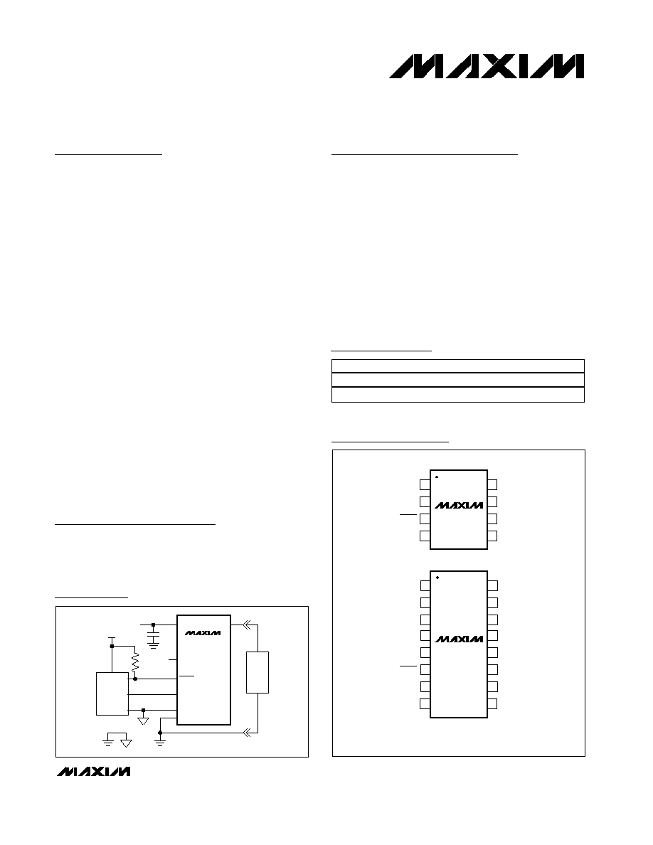
AGND
ENABLE
DGND
1
2
8
7
UVLO
V
OUT
V
IN
FAULT
GATE
8 SO
TOP VIEW
3
4
6
5
MAX5911
V
OUT
V
IN
N.C.*
1
2
13
12
N.C.*
UVLO
N.C.*
16 SO
6
7
11
10
MAX5912
3
4
5
8
16
15
14
9
ENABLE
N.C.*
V
IN
AGND
V
IN
GATE
V
IN
N.C.*
DGND
FAULT
*THESE PINS ARE NOT INTERNALLY CONNECTED.
Pin Configurations
V
IN
FAULT
ENABLE
DGND
UVLO
AGND
POSITIVE
LOGIC
0.1
µF
3.3k
+3.3V
V
OUT
LOAD
V
IN
(-48V)
MAX5911
MAX5912
AGND
DGND
Typical Operating Circuit
19-1832; Rev 0a; 1/01
For price, delivery, and to place orders, please contact Maxim Distribution at 1-888-629-4642,
or visit Maxim's website at www.maxim-ic.com.
Ordering Information
Simple Swapper is a trademark of Maxim Integrated Products, Inc.
PART
TEMP. RANGE
PIN-PACKAGE
MAX5911ESA
-40
∞C to +85∞C
8 SO
MAX5912ESE
-40
∞C to +85∞C
16 SO
IP Phones
Network Routers
Network Switches
Internet Appliances
Power-Over-LAN
MAX5911/MAX5912
-48V Simple Swapper Hot-Swap Switches
2
_______________________________________________________________________________________
ABSOLUTE MAXIMUM RATINGS
ELECTRICAL SPECIFICATIONS
(V
IN
= -48V, AGND = DGND = 0, UVLO = open circuit, V
ENABLE
= +3.3V, and T
A
= -40∞C to +85∞C, unless otherwise noted. Typical
values are at T
A
= +25∞C.)
Stresses beyond those listed under "Absolute Maximum Ratings" may cause permanent damage to the device. These are stress ratings only, and functional
operation of the device at these or any other conditions beyond those indicated in the operational sections of the specifications is not implied. Exposure to
absolute maximum rating conditions for extended periods may affect device reliability.
V
IN
..........................................................................+0.3V to -70V
V
OUT
............................................................+0.3V to (V
IN
- 0.3V)
ENABLE to DGND ..................................................-0.3V to +11V
ENABLE to V
IN
.......................................................-0.3V to +70V
FAULT to DGND .....................................................-0.3V to +11V
UVLO to V
IN
............................................................-0.3V to +11V
DGND ..........................................................................-5V to +5V
DGND to V
IN
...........................................................-0.3V to +70V
FAULT Sink Current ............................................................10mA
Continuous Output Current ...............................Internally Limited
Continuous Power Dissipation (T
A
= +70∞C)
8-Pin SO (derate 5.9mW/∞C above +70∞C)..................470mW
16-Pin SO (derate 12.9mW/∞C above +70∞C)...........1039mW
Operating Temperature Range ...........................-40∞C to +85∞C
Junction Temperature ......................................................+150∞C
Storage Temperature Range .............................-60∞C to +150∞C
Lead Temperature (soldering, 10s) .................................+300∞C
PARAMETER
SYMBOL
CONDITIONS
MIN
TYP
MAX
UNITS
Input Voltage Range
V
IN
-65
-16
V
Supply Current
I
IN
Measured at AGND at the end of output
voltage slew
1.5
2.5
mA
MAX5911
-310
-280
-250
Maximum V
OUT
Current
I
OUT(MAX)
V
OUT
= V
IN
+ 5V
MAX5912
-457
-415
-373
mA
DMOS On-Resistance
R
DS(ON)
MAX5911 I
OUT
= -225mA,
MAX5912 I
OUT
= -350mA
2.5
4
V
OUT
Leakage Current
Measured on V
OUT
when internal DMOS is
shut off
10
µA
ENABLE Low
Voltage
V
IL
Referenced to DGND
0.8
V
ENABLE High Voltage
V
IH
Referenced to DGND
2.0
V
ENABLE High Input Current
I
IH
V
ENABLE
= +3.3V
140
300
µA
ENABLE Low Pulse Width
(Note 1)
t
EPW
200
ns
FAULT Output Low Voltage
V
OL
I
FAULT
= 3mA
0.4
V
FAULT Output Leakage Current
I
OH
V
FAULT
= +3.3V
10
µA
Zero-Current Detection
Threshold
IF
TH
Decreasing load current
-12
-8
-4
mA
Zero-Current Detection
Threshold Hysteresis
IF
HY
1.5
mA
Zero-Current Detection Delay
(Note 2)
IF
DEL
280
350
520
ms
Current-Limit Delay (Note 3)
t
LIMIT
V
OUT
shorted to AGND
10
20
µs
Power-Good Threshold
V
PG
|V
IN
- V
OUT
|, |V
IN
- V
OUT
| decreasing
1.95
2.15
2.35
V
Power-Good Hysteresis
PG
HYS
% of V
PG
5
%
Voltages are with respect to AGND, unless otherwise noted.
MAX5911/MAX5912
-48V Simple Swapper Hot-Swap Switches
_______________________________________________________________________________________
3
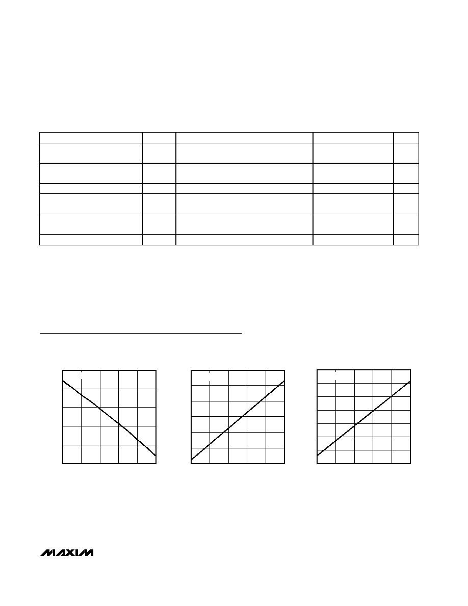
0.8
1.0
1.4
1.2
1.6
1.8
-65
-45
-55
-35
-25
-15
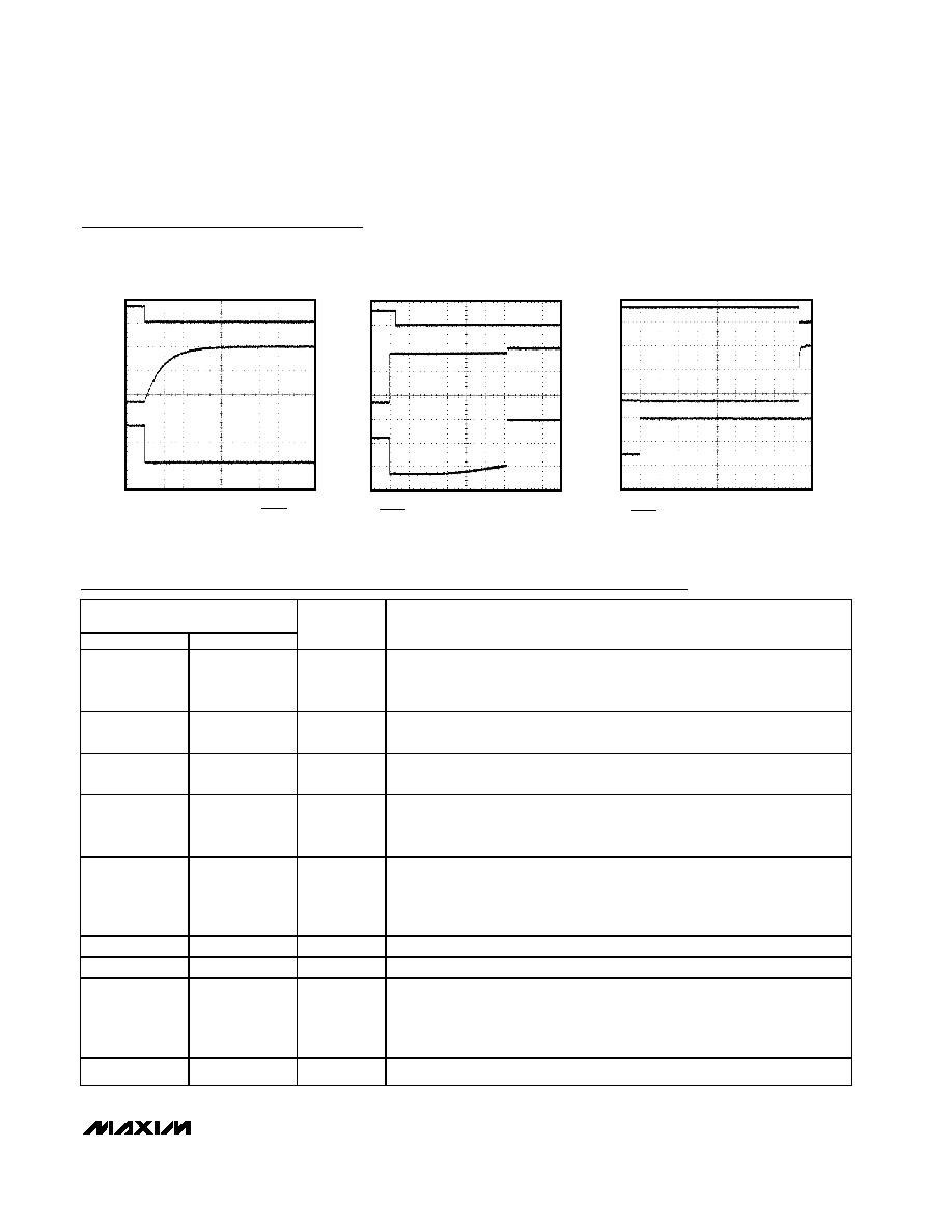
SUPPLY CURRENT
vs. SUPPLY VOLTAGE
MAX5911 toc01
SUPPLY VOLTAGE (V)
SUPPLY CURRENT (mA)
NO LOAD
1.510
1.520
1.515
1.530
1.525
1.535
1.540
-40
10
-15
35
60
85
SUPPLY CURRENT
vs. AMBIENT TEMPERATURE
MAX5911 toc02
TEMPERATURE (
∞C)
SUPPLY CURRENT (mA)
NO LOAD
1.6
2.0
1.8
2.4
2.2
2.8
2.6
3.0
-40
10
-15
35
60
85
ON-RESISTANCE
vs. AMBIENT TEMPERATURE
MAX5911 toc03
TEMPERATURE (
∞C)
ON-RESISTANCE (
)
I
LOAD
= 150mA
Typical Operating Characteristics
(V
IN
= -48V, AGND = DGND = 0, UVLO = open circuit, V
ENABLE
= +3.3V, R
LOAD
= 1.8k
, T
A
= +25∞C, unless otherwise noted.)
ELECTRICAL SPECIFICATIONS (continued)
(V
IN
= -48V, AGND = DGND = 0, UVLO = open circuit, V
ENABLE
= +3.3V, and T
A
= -40∞C to +85∞C, unless otherwise noted. Typical
values are at T
A
= +25∞C.)
Note 1: Minimum ENABLE low pulse width required to unlatch fault condition.
Note 2: The delay from I
OUT
falling below the zero-current threshold until FAULT is latched low and V
OUT
is disabled.
Note 3: The time from an output overcurrent or short-circuit condition until the output goes into current limit.
Note 4: The time from V
OUT
falling until FAULT is asserted low. FAULT is not latched for Power-Not-Good condition.
Note 5: When the device goes into thermal shutdown, the output is disabled and FAULT is latched low.
PARAMETER
SYMBOL
CONDITIONS
MIN
TYP
MAX
UNITS
Power-Not-Good Output Delay
(Note 4)
PG
DEL
After |V
IN
- V
OUT
| increases above
(V
PG
+ PG
HYS
)
8
14
20
ms
Thermal Shutdown Temperature
(Note 5)
T
J
140
o
C
Default UVLO
UVLO open circuit, |V
IN
| increasing
-30
-28
-26
V
UVLO Hysteresis
UVLO open circuit, percentage of UVLO
threshold
12
%
UVLO Comparator Threshold
Referenced to V
IN
, UVLO open circuit,
|V
IN
| increasing
+1.258
V
UVLO Input Resistance
R
UVLO
95
k
MAX5911/MAX5912
-48V Simple Swapper Hot-Swap Switches
4
_______________________________________________________________________________________
Typical Operating Characteristics (continued)
(V
IN
= -48V, AGND = DGND = 0, UVLO = open circuit, V
ENABLE
= +3.3V, R
LOAD
= 1.8k
, T
A
= +25∞C, unless otherwise noted.)
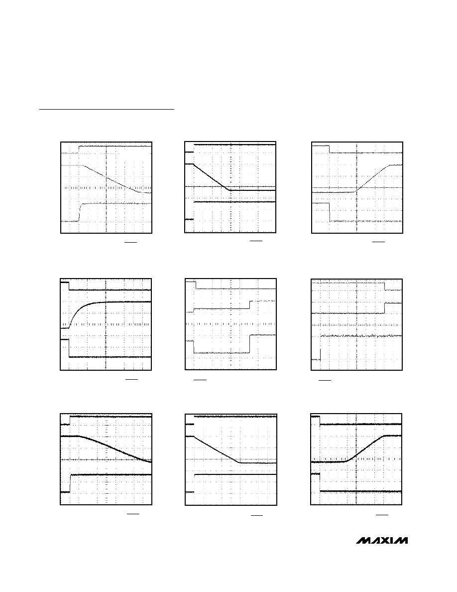
0
MAX5911 TURN-OFF WAVEFORMS
(R
L
= 1.8k
, C
L
= NONE)
MAX5911 toc06
t = 10
µs/div
0
0
A
B
C
A: ENABLE, 5V/div C: FAULT, 2V/div
B: V
OUT
, 20V/div
t = 100ms/div
MAX5911 TURN-OFF WAVEFORMS
(R
L
= 1.8k
, C
L
= 47µF)
A: ENABLE, 5V/div C: FAULT, 2V/div
B: V
OUT
, 20V/div
A
B
C
0
MAX5911 toc07
0
0
0
MAX5911 TURN-ON WAVEFORMS
(R
L
= 1.8k
, C
L
= NONE)
MAX5911 toc04
t = 10
µs/div
0
0
A
B
C
A: ENABLE, 5V/div
B: V
OUT
, 20V/div
C: FAULT, 2V/div
t = 2ms/div
MAX5911 TURN-ON WAVEFORMS
(R
L
= 1.8k
, C
L
= 47µF)
A: ENABLE, 5V/div C: FAULT, 2V/div
B: V
OUT
, 20V/div
A
B
C
0
MAX5911 toc05
0
0
0
MAX5911
OVERCURRENT RESPONSE
MAX5911 toc08
t = 50ms/div
0
0
A
B
C
B: V
OUT
, 50V/div
A: FAULT, 5V/div C: I
OUT
, 200mA/div
0
MAX5911
ZERO-CURRENT RESPONSE
MAX5911 toc09
t = 50ms/div
0
0
A
B
C
B: V
OUT
, 50V/div
A: FAULT, 5V/div C: I
OUT
, 50mA/div
t = 10µs/div
MAX5912 TURN-ON WAVEFORMS
(R
L
= 1.8k
, C
L
= NONE)
A: ENABLE, 5V/div C: FAULT, 2V/div
B: V
OUT
, 20V/div
A
B
C
0
MAX5911 toc10
0
0
t = 1ms/div
MAX5912 TURN-ON WAVEFORMS
(R
L
= 1.8k
, C
L
= 47µF)
A
B
C
0
MAX5911 toc11
0
A: ENABLE, 5V/div C: FAULT, 2V/div
B: V
OUT
, 20V/div
0
t = 10µs/div
MAX5912 TURN-OFF WAVEFORMS
(R
L
= 1.8k
, C
L
= NONE)
A: ENABLE, 5V/div C: FAULT, 2V/div
B: V
OUT
, 20V/div
A
B
C
0
MAX5911 toc12
0
0
MAX5911
/
MAX5912
-48V Simple Swapper Hot-Swap Switches
_______________________________________________________________________________________
5
Pin Description
PIN
MAX5911
MAX5912
NAME
FUNCTION
1
3
GATE
Gate of the Internal Power MOSFET. Normally leave open circuit. To slow
down the output voltage ramp, connect two capacitors, one to V
IN
and one to
V
OUT
. See GATE Connections for details.
2
4, 5, 12, 13
V
IN
Voltage Input Terminal. Bypass V
IN
, to AGND with a 0.1µF capacitor to
improve noise immunity.
3
6
FAULT
Fault Logic Output, open-drain. Tie
FAULT to the positive logic supply with a
3.3k
resistor. Referenced to DGND.
4
7
DGND
Digital Ground. Ground reference level for the external positive logic,
FAULT,
and ENABLE. DGND can vary up to
±5V with respect to AGND to
accommodate differential ground voltages in large systems.
5
10
ENABLE
ENABLE Input. Turns on and off the internal FET. ENABLE is a positive logic-
level input referenced to DGND. Drive ENABLE high to enable V
OUT
. Drive
ENABLE low to disable V
OUT
. Pulse ENABLE low to reset the MAX5911/
MAX5912 after a latched fault condition occurs.
6
11
AGND
Analog Ground. Ground reference level for V
IN
, V
OUT
, and UVLO.
7
14
V
OUT
Voltage Output Terminal
8
15
UVLO
Undervoltage Lockout Input. Leave UVLO open circuit for default setting
of -28V. Alternatively, UVLO can be connected to a resistive divider to set the
lockout voltage (see the Changing the Undervoltage Lockout Setting section).
The comparator threshold level is +1.258V with respect to V
IN
.
--
1, 2, 8, 9, 16
N.C.
No Connection. No internal connection.
t = 100ms/div
MAX5912 TURN-OFF WAVEFORMS
(R
L
= 1.8k
, C
L
= 47µF)
A: ENABLE, 5V/div C: FAULT, 2V/div
B: V
OUT
, 20V/div
A
B
C
0
MAX5911 toc13
0
0
Typical Operating Characteristics (continued)
(V
IN
= -48V, AGND = DGND = 0, UVLO = open circuit, V
ENABLE
= +3.3V, R
LOAD
= 1.8k
, T
A
= +25∞C, unless otherwise noted.)
t = 40ms/div
MAX5912
OVERCURRENT RESPONSE
A: FAULT, 5V/div C: I
OUT
, 200mA/div
B: V
OUT
, 20V/div
A
B
C
0
MAX5911 toc14
0
0
t = 40ms/div
MAX5912
ZERO-CURRENT RESPONSE
A: FAULT, 5V/div C: I
OUT
, 100mA/div
B: V
OUT
, 20V/div
A
B
C
0
MAX5911 toc15
0
0