 | –≠–ª–µ–∫—Ç—Ä–æ–Ω–Ω—ã–π –∫–æ–º–ø–æ–Ω–µ–Ω—Ç: MAX5915 | –°–∫–∞—á–∞—Ç—å:  PDF PDF  ZIP ZIP |

General Description
The MAX5915/MAX5916 dual PCI 2.2 hot-swap con-
trollers allow for safe insertion and removal of two PCI
cards into live PCI slots or backplanes by limiting the
inrush current at startup. After startup, the
MAX5915/MAX5916 provide protection against short-
circuit, overcurrent, and undervoltage conditions.
The MAX5915/MAX5916 provide independent power
controls for +3.3V, +5V,
±12V, and +3.3V auxiliary sup-
plies of two PCI cards. The MAX5915/MAX5916 provide
intelligent selective thermal shutdown control that shuts
down the channel with an overcurrent fault. Both the
MAX5915 and MAX5916 include internal power
MOSFETs for the +12V, -12V, and +3.3V auxiliary out-
puts. The MAX5915/MAX5916 use internal charge
pumps to activate the gates of the internal FETs control-
ling the +3.3V auxiliary supply. Internal FETs and current-
sense circuitry regulate the
±12V and the +3.3V auxiliary
supplies. Channels A and B operate independently,
allowing a single MAX5915/MAX5916 to monitor two PCI
card slots.
The MAX5915 offers latched fault protection and the
MAX5916 offers autorestart fault protection. The
devices are available in the low-profile 28-pin TSSOP
package and are specified over the -40
∞C to +85∞C
extended temperature range.
Applications
PCI 2.2 Server
PCI Server
RAID
Features
o PCI 2.2 Compliant
o Independent Power Controls for +3.3V, +5V, ±12V,
and +3.3V Auxiliary Supplies of Two PCI Cards
o Internal MOSFET Switches for ±12V and +3.3V
Auxiliary Outputs
o Separate ON/OFF Control Input for Each Channel
o Independent +3.3V Auxiliary Output ON/OFF
Control
o Overcurrent Foldback with Timeout and Shutdown
Protection for
±12V and +3.3V Auxiliary Rails with
Status Report
o Brick Wall with Timeout and Shutdown Protection
for +5V and +3.3V Rails with Status Report
o Output Undervoltage Monitoring for +3.3V, +5V,
+12V, and +3.3V Auxiliary Rails with Status Report
o +3.3V Auxiliary Autorestart
o Intelligent Selective Thermal Shutdown Control
Shuts Down Only the Channel with an Overcurrent
Fault
o 28-Pin TSSOP Package
MAX5915/MAX5916
Dual PCI 2.2 Hot-Swap Controllers
________________________________________________________________ Maxim Integrated Products
1
19-2420; Rev 0; 4/02
For pricing, delivery, and ordering information, please contact Maxim/Dallas Direct! at
1-888-629-4642, or visit Maxim's website at www.maxim-ic.com.
Ordering Information
PART
FAULT
MANAGEMENT
TEMP
RANGE
PIN-
PACKAGE
MAX5915EUI
Latched
-40
∞C to +85∞C 28 TSSOP
MAX5916EUI
Autorestart
-40
∞C to +85∞C 28 TSSOP
Pin Configuration, Functional Diagram, and Typical Operating
Circuit appear at end of data sheet.
Typical Application Circuit
+12VIN
+3.3V
+5V
-12VIN
3.3VGATE_
3.3VSEN_
3.3VO_
5VGATE_
5VSEN_
FAIRCHILD
FDS6670A
FAIRCHILD
FDS6670A
0.005
0.005
10k
10k
5VO_
5V
470
µF
47
µF
3.3VAUXIN
3.3VAUXO_
PGOOD_
GND
ON_
ON
OFF
AUXON_
+12VO_
-12VO_
MAX5915
MAX5916
470
µF
4.7
µF 0.1µF
ON
OFF
4.7
µF 0.1µF
4.7
µF 0.1µF
47
µF
47
µF
-12V
+12V
+3.3VAUX
MAX5915/MAX5916
Dual PCI 2.2 Hot-Swap Controllers
2
_______________________________________________________________________________________
ABSOLUTE MAXIMUM RATINGS
Stresses beyond those listed under "Absolute Maximum Ratings" may cause permanent damage to the device. These are stress ratings only, and functional
operation of the device at these or any other conditions beyond those indicated in the operational sections of the specifications is not implied. Exposure to
absolute maximum rating conditions for extended periods may affect device reliability.
+12VIN to GND ...................................................-0.3V to +14.0V
-12VIN to GND........................................................-14V to +0.3V
-12VO_ to GND......................................+0.3V to (V
-12VIN
- 0.3V)
+12VO_, 3.3VGATE_, 5VGATE_
to GND..................................................-0.3V to (V
+12VIN
+ 0.3V)
Any Other Pin to GND ...........................................-0.3V to +6.0V
Continuous Power Dissipation (T
A
= +70
∞C)
28-Pin TSSOP (derate 23.8mW/
∞C above +70∞C) ...........1.9W
Maximum Junction Temperature .....................................+150∞C
Storage Temperature Range .............................-65∞C to +150∞C
Lead Temperature (soldering, 10s) .................................+300∞C
ELECTRICAL CHARACTERISTICS
(V
-12VIN
= -12V, V
+12VIN
= +12V, V
3.3VAUXIN
= +3.3V, V
ON_
= V
AUXON_
= +5V, T
A
= -40
∞C to +85∞C, unless otherwise specified.
Typical values are at T
A
= +25
∞C.)
PARAMETER
SYMBOL
CONDITIONS
MIN
TYP
MAX
UNITS
POWER SUPPLIES
Main Supply Input Voltage
Range
V
+12VIN
10.8
12
13.2
V
Main Supply Undervoltage
Lockout (UVLO)
V
+12UVLO
V
+12VIN
rising
9.6
10
10.8
V
Main Supply UVLO Hysteresis
V
UVLO, HYS
100
mV
Main Input UVLO Delay Time
t
DEG, UVLO
Figures 1 and 2 (Note 1)
1.6
ms
Supply Current
I
Q
2.5
5.0
mA
+3.3V SUPPLY CONTROL
Gate Charge Current
I
3.3VGATE_, CHG
V
3 .3 V GAT E
_ = + 6V , V
3 .3 V S E N _
= + 3.3V ,
V
3 .3 V O
_ = + 3.3V
5
15
30
µA
Gate Discharge Current
I
3.3VGATE_, DIS
V
3.3VGATE
_ = +12V, V
ON_
= 0
50
150
250
µA
Gate High Voltage
V
3.3VGATE_, HIGH
I
3.3VGATE
_ = 1
µA
V
+12VIN
-
0.5
V
+12VIN
V
Gate Low Voltage
V
3.3VGATE_, LOW
I
3.3VGATE
_ = 1
µA, V
ON
_ = 0
0.1
0.4
V
3.3VO_ Input Bias Current
I
3.3VO_, BIAS
V
3.3VO
_ = +3.3V
20
µA
3.3VO_ Internal Pulldown
R
PD
V
ON
_ = 0
1
k
3.3VSEN_ Input Bias Current
I
3.3VSEN_, BIAS
V
3.3VSEN
_ = +3.3V
10
µA
Current-Limit Threshold
V
3.3V, LIM
V
3.3VGATE
_ = +6V
41
46
51
mV
Output Undervoltage Threshold
V
3.3VIN, UV
V
3.3VGATE
_ falling
2.79
2.89
2.99
V
Output Undervoltage Threshold
Hysteresis
30
mV
MAX5915/MAX5916
Dual PCI 2.2 Hot-Swap Controllers
_______________________________________________________________________________________
3
ELECTRICAL CHARACTERISTICS (continued)
(V
-12VIN
= -12V, V
+12VIN
= +12V, V
3.3VAUXIN
= +3.3V, V
ON_
= V
AUXON_
= +5V, T
A
= -40
∞C to +85∞C, unless otherwise specified.
Typical values are at T
A
= +25
∞C.)
PARAMETER
SYMBOL
CONDITIONS
MIN
TYP
MAX
UNITS
+5V SUPPLY CONTROL
Gate Charge Current
I
5VGATE
_
, CHG
V
5VGATE
_ = +6V, V
5VSEN
_ = +5V,
V
5VO
_ = +5V
5
15
30
µA
Gate Discharge Current
I
5VGATE
_
, DIS
V
5VGATE
_ = +12V, V
ON
_ = 0
50
150
250
µA
Gate High Voltage
V
5VGATE
_
, HIGH
I
5VGATE
_ = 1
µA
V
+12VIN
-
0.5V
V
+12VIN
V
Gate Low Voltage
V
5VGATE
_
, LOW
I
5VGATE
_ = 1
µA, V
ON
_ = 0
0.1
0.4
V
5VO_ Input Bias Current
I
5VO
_
, BIAS
V
5VO
_ = +5V
20
µA
5VO_ Internal Pulldown
R
5VO
_
, PD
V
ON
_ = 0
1
k
5VSEN_ Input Bias Current
I
5VSEN
_
, BIAS
V
5VSEN
_ = +5V
10
µA
Current-Limit Threshold
V
5VO
_
, LIM
V
5VGATE
_ falling
27
31
35
mV
Output Undervoltage Threshold
V
5VO
_
, UV
Output falling
4.34
4.50
4.70
V
Output Undervoltage Threshold
Hysteresis
45
mV
+12V SUPPLY CONTROL
T
A
= +25
∞C, I
D
= 0.5A
0.32
0.38
On-Resistance of Internal Switch
R
DS(ON), +12V
T
A
= +85
∞C, I
D
= 0.5A
0.5
Foldback Current Limit
I
+12VIN, LIM
V
+12VO
_ = 0
0.68
1
1.36
A
Current-Foldback Threshold
Output current rising (Note 2)
1.4
A
Output Undervoltage Threshold
V
+12VO
_
, UV
Output falling
10.00
10.4
10.82
V
+12VO_ Internal Pulldown
R
+12VO
_
, PD
V
ON
_ = 0
1
k
-12V SUPPLY CONTROL
T
A
= +25
∞C, I
D
= 0.1A
0.58
0.9
On-Resistance of Internal Switch
R
DS(ON), -12V
T
A
= +85
∞C, I
D
= 0.1A
1.3
Foldback Current Limit
I
-12VIN, LIM
V
-12VO_
= 0
136
205
273
mA
Current-Foldback Threshold
Output current rising (Note 2)
240
mA
-12VO_ Internal Pullup
R
-12VO_, PU
V
ON_
= 0
1
k
+3.3VAUX SUPPLY CONTROL
Input Voltage Range
V
3.3VAUXIN
3.0
3.3
3.6
V
3.3VAUXIN Undervoltage
Lockout
V
UVLO, AUX
Input rising
2.65
2.75
2.85
V
Hysteresis
V
UVLO-AUX, HYS
30
mV
Supply Current
I
Q, 3.3VAUX
1
2
mA
MAX5915/MAX5916
Dual PCI 2.2 Hot-Swap Controllers
4
_______________________________________________________________________________________
ELECTRICAL CHARACTERISTICS (continued)
(V
-12VIN
= -12V, V
+12VIN
= +12V, V
3.3VAUXIN
= +3.3V, V
ON_
= V
AUXON_
= +5V, T
A
= -40
∞C to +85∞C, unless otherwise specified.
Typical values are at T
A
= +25
∞C.)
PARAMETER
SYMBOL
CONDITIONS
MIN
TYP
MAX
UNITS
T
A
= +25
∞C, I
D
= 0.4A
0.24
0.4
On-Resistance of Internal Switch
R
DS(ON), 3.3VAUX
T
A
= +85
∞C, I
D
= 0.4A
0.6
Foldback Current Limit
I
3.3VAUXIN, LIM
V
3.3VAUXO
_ = 0
0.5
0.75
1.0
A
Current-Foldback Threshold
Output current rising (Note 2)
1.2
A
Output Undervoltage Threshold
V
3.3VAUXIN, UV
2.76
2.89
2.99
V
Auxiliary Input UVLO Delay Time
t
DEG, UVLO
(Note 1)
1.6
ms
3.3VAUXO_ Internal Pulldown
R
3.3VAUXO_
ON_ = 0
1
k
ON AND AUXON COMPARATORS
Threshold Voltage
1.0
2.1
V
Hysteresis
V
HYS
25
mV
Input Bias Current
I
B, COMP
20
µA
ON_ and AUXON_ Deglitch
Time
t
DEG
Figures 5≠8 (Note 3)
4
µs
FAULT RESPONSE, PGOOD_ STATUS OUTPUT
PGOOD_ Output Overcurrent
and Undervoltage Response
Time
t
RESP
Figures 5≠8
0.5
1.5
ms
Output Overcurrent and
Undervoltage Deglitch Time
t
DELAY
Figures 3≠7
16
t
RESP
ms
PGOOD_ Startup Time Out
t
START
See Figures 1, 2, 5, 6, 7, and 8
4
t
DELAY
ms
Autorestart Delay
t
RESTART
Delay time to restart after OC and/or
UV shutdown
64
t
START
ms
PGOOD_ Output Low Voltage
V
OL
I
SINK
= 2mA, ON_ = 0
0.5
0.7
V
PGOOD_ Output High Leakage
Current
I
LEAK
V
PGOOD_
= +5.5V
1
µA
Thermal Shutdown Threshold
T
SD
(Note 4)
125
∞C
Thermal Shutdown Hysteresis
T
HYS
5
∞C
Full Thermal Shutdown
Threshold
T
SD, FULL
(Note 5)
T
SD
+
20
∞C
Full Thermal Shutdown
Hysteresis
T
HYS, FULL
5
∞C
Note 1: t
DEG, UVLO
is negative edge triggered. There is no time delay when the inputs rise above the UVLO threshold.
Note 2: The current threshold when the output current starts to fold back. See the Typical Operating Characteristics.
Note 3: t
DEG
is negative edge triggered. ON_ or AUXON_ transition from low to high has no delay.
Note 4: Temperature threshold at which the outputs of the channel with overcurrent shut down.
Note 5: The temperature threshold at which both channels shut down.
MAX5915/MAX5916
Dual PCI 2.2 Hot-Swap Controllers
_______________________________________________________________________________________
5
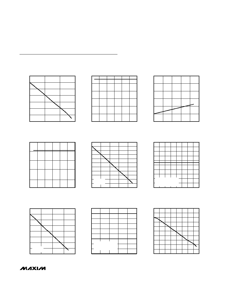
Typical Operating Characteristics
(V
+12VIN
= +12V, V
3.3VAUXIN
= +3.3V, V
-12VIN
= -12V, V
5V
= +5V, V
3.3V
= +3.3V, R
5VSEN_
= 0.005
, R
3.3VSEN_
= 0.005
, C
3.3VO_
=
C
5VO_
= 470µF, C
+12VO_
= C
-12VO_
= C
3.3VAUXO_
= 47µF, T
A
= +25
∞C, unless otherwise noted. See Typical Application Circuit.)
MAX5915 toc09
OUTPUT CURRENT (A)
3.3VAUX_ VOLTAGE (V)
1.05
0.90
0.60 0.75
0.30 0.45
0.15
2.6
2.7
2.8
2.9
3.0
3.1
3.2
3.3
3.4
3.5
2.5
0
1.20
3.3VAUX_ VOLTAGE
vs. OUTPUT CURRENT
3.3VO_ SENSE RESISTOR VOLTAGE
vs. DIFFERENTIAL SWITCH VOLTAGE
MAX5915 toc08
V
IN
- V
3.3VSEN_
(V)
3.3VO_ CURRENT-LIMIT THRESHOLD (mV)
30
34
32
36
38
42
46
44
48
40
3.0
2.5
1.5
2.0
1.0
3.5
DURING CURRENT LIMIT
FAIRCHILD
FDS6670A
3.3VO_ VOLTAGE
vs. OUTPUT CURRENT
MAX5915 toc07
OUTPUT CURRENT (A)
3.3VO_ VOLTAGE (V)
2
3.18
3.20
3.22
3.28
3.30
3.32
3.16
0
8
4
6
3.24
3.26
FAIRCHILD
FDS6670A
20
24
22
28
26
30
34
38
36
40
1.0
1.5
2.0
2.5
3.0
3.5
4.0
4.5
5.0
5VO_ SENSE RESISTOR VOLTAGE
vs. DIFFERENTIAL SWITCH VOLTAGE
MAX5915 toc06
V
IN
- V
5VSEN_
(V)
5VO_ CURRENT-LIMIT THRESHOLD (mV)
32
DURING CURRENT LIMIT
FAIRCHILD
FDS6670A
5VO_ VOLTAGE
vs. OUTPUT CURRENT
MAX5915 toc05
OUTPUT CURRENT (A)
5VO_ VOLTAGE (V)
1
4.82
4.84
4.86
4.88
4.90
4.92
4.80
0
5
2
3
4
4.94
4.96
4.98
5.00
5.02
FAIRCHILD
FDS6670A
-12VO_ CURRENT FOLDBACK
vs. DIFFERENTIAL SWITCH VOLTAGE
MAX5915 toc04
V
-12VIN
- V
-12VO_
(V)
-12VO_ CURRENT FOLDBACK (mA)
2
50
100
150
200
250
0
0
4
6
8
10
12
-12VO_ VOLTAGE
vs. OUTPUT CURRENT
MAX5915 toc03
OUTPUT CURRENT (mA)
-12VO_ VOLTAGE (V)
50
-12.0
-11.9
-11.8
-11.7
-11.6
-11.5
-12.1
0
250
100
150
200
+12VO_ CURRENT FOLDBACK
vs. DIFFERENTIAL SWITCH VOLTAGE
MAX5915 toc02
V
+12VIN
- V
+12VO_
(V)
+12VO_ CURRENT FOLDBACK (A)
2
0.1
0.3
0.5
0.7
0.9
1.1
-0.1
0
4
6
8
10
12
+12VO_ VOLTAGE
vs. OUTPUT CURRENT
MAX5915 toc01
OUTPUT CURRENT (A)
+12VO_ VOLTAGE (V)
1.0
0.5
11.5
11.6
11.7
11.8
11.9
12.0
12.1
11.4
0
1.5