 | ÐлекÑÑоннÑй компоненÑ: MAX5931 | СкаÑаÑÑ:  PDF PDF  ZIP ZIP |
Äîêóìåíòàöèÿ è îïèñàíèÿ www.docs.chipfind.ru
General Description
The MAX5930/MAX5931 +1V to +13.2V triple hot-swap
controllers provide complete protection for multisupply
systems. They allow the safe insertion and removal of
circuit cards into live backplanes. These devices hot
swap multiple supplies ranging from +1V to +13.2V,
provided one supply is at or above +2.7V and only one
supply is above 11V. The input voltage rails (channels)
can be configured to sequentially turn-on/off, track
each other, or have completely independent operation.
The discharged filter capacitors of the circuit card pro-
vide low impedance to the live backplane. High inrush
currents from the backplane to the circuit card can burn
up connectors and components, or momentarily collapse
the backplane power supply leading to a system reset.
The MAX5930/MAX5931 hot-swap controllers prevent
such problems by gradually ramping up the output volt-
age and regulating the current to a preset limit when the
board is plugged in, allowing the system to stabilize
safely. After the startup cycle is complete, on-chip com-
parators provide VariableSpeed/BiLevelTM protection
against short-circuit and overcurrent faults, and provide
immunity against system noise and load transients.
The load is disconnected in the event of a fault condi-
tion. The MAX5930/MAX5931 fault-management mode
is selectable, allowing latched fault or autoretry after a
fault condition.
The MAX5930/MAX5931 offer a variety of options to
reduce external component count and design time. All
devices integrate an on-board charge pump to drive
the gates of low-cost, external N-channel MOSFETs, an
adjustable startup timer, and an adjustable current limit.
The devices offer integrated features like startup cur-
rent regulation and current glitch protection to eliminate
external timing resistors and capacitors. The
MAX5931L provides an open-drain, active-low status
output for each channel, the MAX5931H provides an
open-drain, active-high status output for each channel,
and the MAX5930 status output polarity is selectable.
The MAX5930 is available in a 24-pin QSOP package,
and the MAX5931 is available in a 20-pin QSOP pack-
age. All devices are specified over the extended -40°C
to +85°C temperature range.
Applications
Features
Safe Hot Swap for +1V to +13.2V Power Supplies
with Any Input Voltage (V
IN_
)
2.7V and Only One
V
IN_
> 11.0V
Adjustable Circuit Breaker/Current-Limit
Threshold from 25mV to 100mV
Configurable Tracking, Sequencing, or
Independent Operation Modes
VariableSpeed/BiLevel Circuit-Breaker Response
Internal Charge Pumps Generate N-Channel
MOSFET Gate Drives
Inrush Current Regulated at Startup
Autoretry or Latched Fault Management
Programmable Undervoltage Lockout
Status Outputs Indicate Fault/Safe Condition
MAX5930/MAX5931
Low-Voltage, Triple, Hot-Swap Controllers/
Power Sequencers/Voltage Trackers
________________________________________________________________ Maxim Integrated Products
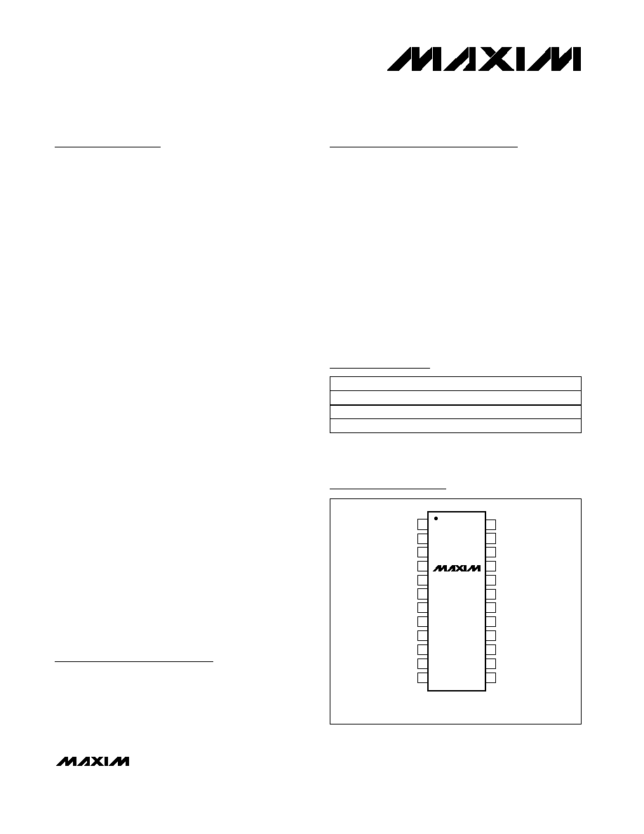
1
24
23
22
21
20
19
18
17
1
2
3
4
5
6
7
8
MODE
ON3
LIM2
IN2
LIM1
ON1
ON2
POL
TOP VIEW
SENSE2
GATE2
LIM3
IN3
STAT1
GATE1
SENSE1
IN1
16
15
14
13
9
10
11
12
SENSE3
GATE3
GND
BIAS
STAT3
LATCH
TIM
STAT2
QSOP
MAX5930
Pin Configurations
Ordering Information
19-3032; Rev 0; 10/03
For pricing, delivery, and ordering information, please contact Maxim/Dallas Direct! at
1-888-629-4642, or visit Maxim's website at www.maxim-ic.com.
PART
TEMP RANGE
PIN-PACKAGE
MAX5930EEG
-40°C to +85°C
24 QSOP
MAX5931LEEP*
-40°C to +85°C
20 QSOP
MAX5931HEEP*
-40°C to +85°C
20 QSOP
VariableSpeed/BiLevel is a trademark of Maxim Integrated
Products, Inc.
Network Switches, Routers,
Hubs
Hot Plug-In Daughter Cards
RAID
Solid-State Circuit Breakers
Power-Supply
Sequencing/Tracking
Base-Station Line Cards
Portable Computer Device
Bays (Docking Stations)
*Future product--contact factory for availability.
Selector Guide and Typical Operating Circuit appear at end
of data sheet.
Pin Configurations continued at end of data sheet.
MAX5930/MAX5931
Low-Voltage, Triple, Hot-Swap Controllers/
Power Sequencers/Voltage Trackers
2
_______________________________________________________________________________________
ABSOLUTE MAXIMUM RATINGS
Stresses beyond those listed under "Absolute Maximum Ratings" may cause permanent damage to the device. These are stress ratings only, and functional
operation of the device at these or any other conditions beyond those indicated in the operational sections of the specifications is not implied. Exposure to
absolute maximum rating conditions for extended periods may affect device reliability.
(All voltages referenced to GND, unless otherwise noted.)
IN_ ..........................................................................-0.3V to +14V
GATE_.............................................................-0.3V to (IN_ + 6V)
BIAS (Note 1) .............................................. (V
IN
- 0.3V) to +14V
ON_, STAT_, LIM_ (MAX5930), TIM, MODE,
LATCH, POL (MAX5930) ..........................-0.3V to (V
IN
+ 0.3V)
SENSE_........................................................-0.3V to (IN_ + 0.3V)
Current into Any Pin..........................................................±50mA
Continuous Power Dissipation (T
A
= +70°C)
20-Pin QSOP (derate 9.1mW/°C above +70°C)............727mW
24-Pin QSOP (derate 9.5mW/°C above +70°C)............762mW
Operating Temperature Range ...........................-40°C to +85°C
Junction Temperature .....................................................+150°C
Storage Temperature Range .............................-65°C to +150°C
Lead Temperature (soldering, 10s) .................................+300°C
ELECTRICAL CHARACTERISTICS
(V
IN_
= +1V to +13.2V provided at least one supply is larger than or equal to +2.7V and only one supply is > 11.0V, T
A
= -40°C to +85°C,
unless otherwise noted. Typical values are at V
IN1
= 12.0V, V
IN2
= 5.0V, V
IN3
= 3.3V, V
ON_
= +3.3V, and T
A
= +25°C.) (Notes 1, 2)
PARAMETER
SYMBOL
CONDITIONS
MIN
TYP
MAX
UNITS
POWER SUPPLIES
IN_ Input Voltage Range
V
IN_
At least one V
IN_
+2.7V and only one
V
IN_
> 11.0V
1.0
13.2
V
Supply Current
I
Q
I
IN1
+ I
IN2
+ I
IN3
, V
ON_
= 2.7V,
V
IN_
= +13.2V, after STAT_ high
2.5
5
mA
CURRENT CONTROL
T
A
= +25°C
22.5
25
27.5
LIM_ = GND
(MAX5930),
MAX5931
(Note 4)
T
A
= -40°C to +85°C
21.0
27.5
R
LIM_
= 10k
(MAX5930)
80
125
Slow-Comparator Threshold
(V
IN_
- V
SENSE_
)
(Note 3)
V
SC,TH
R
LIM_
from LIM_ to GND (MAX5930)
R
LIM_
x 7.5 x
10
-6
+ 25mV
mV
1mV overdrive
3
ms
Slow-Comparator Response Time
(Note 4)
t
SCD
50mV overdrive
130
µs
Fast-Comparator Threshold
(V
IN_
- V
SENSE_
)
V
FC,TH
2 x
V
SC,TH
mV
Fast-Comparator Response Time
t
FCD
10mV overdrive, from overload condition
200
ns
SENSE_ Input Bias Current
I
B SENSE_
V
SENSE_
= V
IN_
0.03
1
µA
MOSFET DRIVER
R
TIM
= 100k
8.0
10.8
13.6
R
TIM
= 4k
(minimum value)
0.30
0.4
0.55
Startup Period (Note 5)
t
START
TIM floating (default)
5
9
14
ms
Note 1: V
IN
is the largest of V
IN1
, V
IN2
, and V
IN3
.
MAX5930/MAX5931
Low-Voltage, Triple, Hot-Swap Controllers/
Power Sequencers/Voltage Trackers
_______________________________________________________________________________________
3
ELECTRICAL CHARACTERISTICS (continued)
(V
IN_
= +1V to +13.2V provided at least one supply is larger than or equal to +2.7V and only one supply is > 11.0V, T
A
= -40°C to +85°C,
unless otherwise noted. Typical values are at V
IN1
= 12.0V, V
IN2
= 5.0V, V
IN3
= 3.3V, V
ON_
= +3.3V, and T
A
= +25°C.) (Notes 1, 2)
PARAMETER
SYMBOL
CONDITIONS
MIN
TYP
MAX
UNITS
Charging, V
GATE_
= GND, V
IN_
= +5V
(Note 6)
80
100
125
Discharging, during startup
100
µA
Discharging, normal turn-off or triggered by
the slow comparator after startup; V
GATE_
=
5V, V
IN_
= 10V, V
ON_
= 0V
2
3
7
Average Gate Current
I
GATE
Discharging, triggered by a fault after
startup; V
GATE_
= 5V, V
IN_
= 10V, (V
IN_
-
V
SENSE_
) > V
FC,TH_
(Note 7)
30
50
120
mA
Gate-Drive Voltage
V
DRIVE
V
GATE_
- V
IN_
, I
GATE_
= 1µA
4.9
5.3
5.6
V
ON COMPARATOR
Low to high
0.85
0.875
0.90
V
ON_ Threshold
V
ON_,TH
Hysteresis
25
mV
ON_ Propagation Delay
10mV overdrive
10
µs
ON_ Voltage Range
V
ON_
Without false output inversion
V
IN
V
ON_ Input Bias Current
I
BON
V
ON_
= V
IN
0.03
1
µA
ON_ Pulse-Width Low
t
UNLATCH
To unlatch after a latched fault
100
µs
DIGITAL OUTPUTS (STAT_)
Output Leakage Current
V
STAT_
13.2V
1
µA
Output Voltage Low
V
OL_
POL = floating (MAX5930), I
SINK
= 1mA
0.4
V
UNDERVOLTAGE LOCKOUT (UVLO)
UVLO Threshold
V
UVLO
Startup is initiated when this threshold is
reached by any V
IN_
and V
ON_
> 0.9V
(Note 8)
2.25
2.45
2.65
V
UVLO Hysteresis
V
UVLO,HYST
250
mV
UVLO Glitch Filter Reset Time
t
D,GF
V
I N
< V
U V L O
m axi m um p ul se w i d th to r eset
10
µs
UVLO to Startup Delay
t
D,UVLO
Time input voltage must exceed V
UVLO
before startup is initiated
20
37.5
60
ms
Input Power-Ready Threshold
V
PWRRDY
Any channel, while V
IN
> V
UVLO
(Note 9)
0.9
0.95
1.0
V
Input Power-Ready Hysteresis
V
PWRHYST
50
mV
LOGIC AND TIMING
POL Input Pullup
I
POL
POL = GND (MAX5930)
2
4
6
µA
LATCH Input Pullup
I
LATCH
LATCH = GND
2
4
6
µA
MODE Input Voltage
V
MODE
MODE floating (default to sequencing
mode)
1.0
1.25
1.5
V
Independent-Mode Selection
Threshold
V
INDEP,TH
V
MODE
rising
0.4
V
Tracking-Mode Selection
Threshold
V
TRACK,TH
V
MODE
rising
2.7
V
MAX5930/MAX5931
Low-Voltage, Triple, Hot-Swap Controllers/
Power Sequencers/Voltage Trackers
4
_______________________________________________________________________________________
ELECTRICAL CHARACTERISTICS (continued)
(V
IN_
= +1V to +13.2V provided at least one supply is larger than or equal to +2.7V and only one supply is > 11.0V, T
A
= -40°C to +85°C,
unless otherwise noted. Typical values are at V
IN1
= 12.0V, V
IN2
= 5.0V, V
IN3
= 3.3V, V
ON_
= +3.3V, and T
A
= +25°C.) (Notes 1, 2)
PARAMETER
SYMBOL
CONDITIONS
MIN
TYP
MAX
UNITS
MODE Input Impedance
R
MODE
200
k
Autoretry Delay
t
RETRY
Delay time to restart after fault shutdown
64 x
t
START
ms
Note 2: All devices are 100% tested at T
A
= +25°C. Limits over temperature are guaranteed by design.
Note 3: The slow-comparator threshold is adjustable. V
SC,TH
= R
LIM
x 7.5µA + 25mV (see the Typical Operating Characteristics).
Note 4: The current-limit slow-comparator response time is weighed against the amount of overcurrent, the higher the overcurrent
condition, the faster the response time (see the Typical Operating Characteristics).
Note 5: The startup period (t
START
) is the time during which the slow comparator is ignored and the device acts as a current-limiter
by regulating the sense current with the fast comparator (see the Startup Period section).
Note 6: The current available at GATE is a function of V
GATE
(see the Typical Operating Characteristics).
Note 7: After a fault triggered by the fast comparator, the gate is discharged by the strong discharge current.
Note 8: Each channel input while the other inputs are at +1V.
Note 9: Each channel input while any other input is at +2.7V.
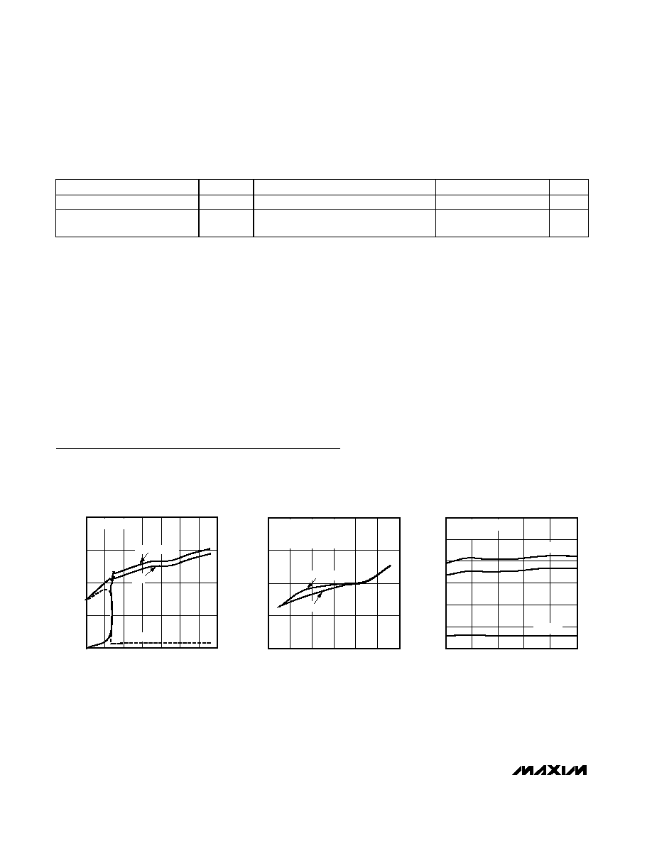
Typical Operating Characteristics
(Typical Operating Circuits, Q1 = Q2 = Q3 = Fairchild FDB7090L, V
IN1
= +12.0V, V
IN2
= +5.0V, V
IN3
= +1V, T
A
= +25°C, unless oth-
erwise noted. Channels 1 through 3 are identical in performance. Where characteristics are interchangeable, channels 1 through 3
are referred to as X, Y, and Z.)
0
1
2
3
4
SUPPLY CURRENT vs. INPUT VOLTAGE
MAX5930 toc01
V
INX
(V)
I
IN
(mA)
0
6
8
2
4
10
12
14
V
INY
= V
INZ
= 2.7V
I
INX
+ I
INY
+ I
INZ
I
INX
I
INY
+ I
INZ
1.0
2.0
3.0
4.0
5.0
2
6
4
8
10
12
14
TOTAL SUPPLY CURRENT
vs. INPUT VOLTAGE
MAX5930 toc02
V
IN
(V)
I
IN
(mA)
I
IN
= I
IN1
+ I
IN2
+ I
IN3
V
IN
= V
INX
= V
INY
= V
INZ
V
ON
= V
ON1
= V
ON2
= V
ON3
V
ON
= 0V
V
ON
= 3.3V
0
1.0
0.5
2.0
1.5
2.5
3.0
-40
85
SUPPLY CURRENT
vs. TEMPERATURE
MAX5930 toc03
TEMPERATURE (
°C)
I
IN
(mA)
10
-15
35
60
I
INY
+ I
INZ
V
ON_
= V
INY
= V
INZ
= 2.7V
V
INX
= 2.8V
I
INY
+ I
INZ
I
INX
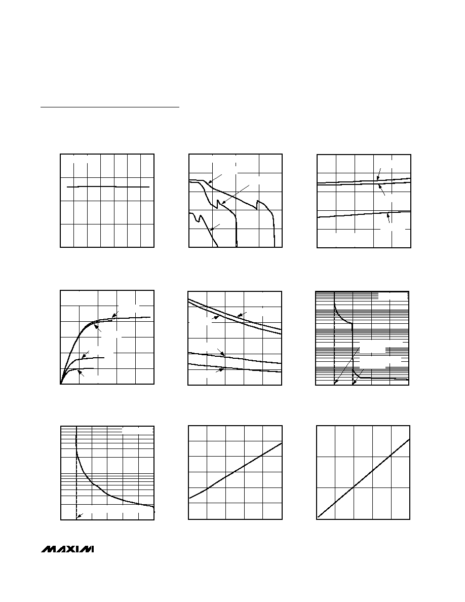
MAX5930/MAX5931
Low-Voltage, Triple, Hot-Swap Controllers/
Power Sequencers/Voltage Trackers
_______________________________________________________________________________________
5
0
2
4
6
8
GATE-DRIVE VOLTAGE
vs. INPUT VOLTAGE
MAX5930 toc04
V
INX
(V)
V
DRIVEX
(V)
0
6
8
2
4
10
12
14
V
INY
= V
INZ
= 2.7V
0
30
90
60
120
150
GATE CHARGE CURRENT
vs. GATE VOLTAGE
MAX5930 toc05
V
GATEX
(V)
GATE CHARGE CURRENT (
µ
A)
0
10
5
15
20
V
ONW
= V
INY
= V
INZ
= 2.7V
V
INX
= 13.2V
V
INX
= 5V
V
INX
= 1V
0
40
120
80
160
200
GATE CHARGE CURRENT
vs. TEMPERATURE
MAX5930 toc06
TEMPERATURE (
°C)
GATE CHARGE CURRENT (
µ
A)
-40
35
10
-15
60
85
V
ONX
= V
INY
= V
INZ
= 2.7V
V
GATEX
= 0V
V
INX
= 13.2V
V
INX
= 5V
V
INX
= 1V
0
2
1
4
3
5
6
0
20
STRONG GATE DISCHARGE CURRENT
vs. GATE VOLTAGE
MAX5930 toc07
V
GATEX
(V)
GATE DISCHARGE CURRENT (mA)
8
4
12
16
V
INX
= 13.2V
V
INX
= 1V
V
INX
= 5V
V
INX
= 3.3V
V
ONX
= 0V
V
INY
= V
INZ
= 2.7V
0
2
1
4
3
5
6
-40
85
STRONG GATE DISCHARGE CURRENT
vs. TEMPERATURE
MAX5930 toc08
TEMPERATURE (
°C)
GATE DISCHARGE CURRENT (mA)
10
-15
35
60
V
INX
= 13.2V
V
INX
= 5V
V
INX
= 3.3V
V
INX
= 1V
V
ONX
= 0V
V
INY
= V
INZ
= 2.7V
10
0
25
50
75
100
125
1
0.1
0.01
0.001
0.0001
TURN-OFF TIME
vs. SENSE VOLTAGE
MAX5930 toc09
V
INX
- V
SENSEX
(mV)
TURN-OFF TIME (ms)
R
LIMX
= 100
SLOW-COMPARATOR
THRESHOLD
FAST-COMPARATOR
THRESHOLD
TURN-OFF TIME vs. SENSE VOLTAGE
(EXPANDED SCALE)
MAX5930 toc10
V
INX
- V
SENSEX
(mV)
TURN-OFF TIME (ms)
10
0.1
1
20
25
30
35
40
45
50
R
LIMX
= 100
SLOW-COMPARATOR THRESHOLD
0
40
20
60
100
80
120
SLOW-COMPARATOR THRESHOLD
vs. R
LIMX
MAX5930 toc11
R
LIMX
(k
)
V
SC,TH
(mV)
0
2
6
4
8
10
0
20
40
60
STARTUP PERIOD
vs. R
TIM
MAX5930 toc12
R
TIM
(k
)
t
START
(ms)
0
100
200
400
300
500
Typical Operating Characteristics (continued)
(Typical Operating Circuits, Q1 = Q2 = Q3 = Fairchild FDB7090L, V
IN1
= +12.0V, V
IN2
= +5.0V, V
IN3
= +1V, T
A
= +25°C, unless oth-
erwise noted. Channels 1 through 3 are identical in performance. Where characteristics are interchangeable, channels 1 through 3
are referred to as X, Y, and Z.)