 | ÐлекÑÑоннÑй компоненÑ: MAX5933B | СкаÑаÑÑ:  PDF PDF  ZIP ZIP |
Äîêóìåíòàöèÿ è îïèñàíèÿ www.docs.chipfind.ru
General Description
The MAX5933AMAX5933F/MAX5947A/B/C fully integrat-
ed hot-swap controllers for +9V to +80V positive supply
rails (MAX5947A/B/C), allow for the safe insertion and
removal of circuit cards into live backplanes without caus-
ing glitches on the backplane power-supply rail. The
MAX5947B is pin- and function-compatible with the
LT1641-2. The other devices offer added features such
as a choice of active-high or active-low power-good out-
puts (PWRGD/PWRGD), latched/autoretry fault manage-
ment, and autoretry duty-cycle options of 3.75% or 0.94%
(see the Selector Guide).
The MAX5933AMAX5933F are available with a default
undervoltage lockout threshold of +31V and operate over
a supply voltage range of +33V to +80V. The
MAX5947A/B/C are available with a default undervoltage
of +8.3V. All devices feature a programmable analog
foldback current limit. If the device remains in current limit
for more than a programmable time, the external
n-channel MOSFET is either latched off (MAX5933A/
MAX5933C/MAX5947A) or is set to automatically restart
after a timeout delay (MAX5933B/MAX5933D/MAX5933E/
MAX5933F/MAX5947B/MAX5947C).
The MAX5933_ and MAX5947_ operate in the extended
temperature range of -40°C to +85°C. These devices are
available in an 8-pin SO package.
Applications
Hot Board Insertion
Electronic Circuit Breakers
Industrial High-Side Switch/Circuit Breakers
Network Routers and Switches
24V/48V Industrial/Alarm Systems
Features
Pin- and Function-Compatible with the LT1641-2
(MAX5947B)
Provides Safe Hot Swap for +9V to +80V Power-
Supply Range (MAX5947A/B/C)
Safe Board Insertion and Removal from Live
Backplanes
Latched/Autoretry Management
Active-Low or Active-High Power-Good Output
Programmable Foldback Current Limiting
High-Side Drive for an External N-Channel MOSFET
Built-In Thermal Shutdown
Undervoltage Lockout (UVLO)
Overvoltage Protection
User-Programmable Supply Voltage
Power-Up Rate
MAX5933AMAX5933F/MAX5947A/B/C
Positive High-Voltage, Hot-Swap Controllers
________________________________________________________________ Maxim Integrated Products
1
Ordering Information
19-3263; Rev 1; 7/04
For pricing, delivery, and ordering information, please contact Maxim/Dallas Direct! at
1-888-629-4642, or visit Maxim's website at www.maxim-ic.com.
Typical Application Circuit and Pin Configuration appear at
end of data sheet.
PART
TEMP RANGE
PIN-PACKAGE
MAX5933_ESA*
-40°C to +85°C
8 SO
MAX5947_ESA*
-40°C to +85°C
8 SO
*Insert the desired suffix from the Selector Guide into the blank
to complete the part number.
PART
LATCHED
FAULT
PROTECTION
AUTORETRY
FAULT
PROTECTION
PWRGD
OUTPUT LOGIC
DUTY CYCLE
(%)
DEFAULT UVLO
(V)
SUPPLY
VOLTAGE
RANGE (V)
MAX5933A
Yes
--
High
--
31
33 to 80
MAX5933B
--
Yes
High
3.75
31
33 to 80
MAX5933C
Yes
--
Low
--
31
33 to 80
MAX5933D
--
Yes
Low
3.75
31
33 to 80
MAX5933E
--
Yes
High
0.94
31
33 to 80
MAX5933F
--
Yes
Low
0.94
31
33 to 80
MAX5947A
Yes
--
Low
--
8.3
9 to 80
MAX5947B
--
Yes
High
3.75
8.3
9 to 80
MAX5947C
--
Yes
Low
3.75
8.3
9 to 80
Selector Guide
MAX5933AMAX5933F/MAX5947A/B/C
Positive High-Voltage, Hot-Swap Controllers
2
_______________________________________________________________________________________
ABSOLUTE MAXIMUM RATINGS
ELECTRICAL CHARACTERISTICS
(V
CC
= +24V (MAX5947A/B/C), V
CC
= +48V (MAX5933AMAX5933F), GND = 0V, T
A
= -40°C to +85°C, unless otherwise noted.
Typical values are at T
A
= +25°C.) (Note 1)
Stresses beyond those listed under "Absolute Maximum Ratings" may cause permanent damage to the device. These are stress ratings only, and functional
operation of the device at these or any other conditions beyond those indicated in the operational sections of the specifications is not implied. Exposure to
absolute maximum rating conditions for extended periods may affect device reliability.
(Voltages Referenced to GND)
V
CC
.........................................................................-0.3V to +85V
SENSE, FB, ON ..........................................-0.3V to (V
CC
+ 0.3V)
TIMER, PWRGD, PWRGD.......................................-0.3V to +85V
GATE ......................................................................-0.3V to +95V
Maximum GATE Current ....................................-50mA, +150mA
Maximum Current into Any Other Pin................................
±50mA
Continuous Power Dissipation (T
A
= +70°C)
8-Pin SO (derate 5.9mW/°C above +70°C)..................470mW
Operating Temperature Range ...........................-40
°C to +85°C
Maximum Junction Temperature .....................................+150°C
Storage Temperature Range .............................-60°C to +150°C
Lead Temperature (soldering, 10s) .................................+300°C
ESD Rating (Human Body Model)......................................2000V
PARAMETER
SYMBOL
CONDITIONS
MIN
TYP
MAX
UNITS
MAX5947A/B/C
9
80
Supply Voltage Range
V
CC
MAX5933AMAX5933F
33
80
V
Supply Current
I
CC
V
ON
= 3V, V
CC
= 80V
1.4
3.5
mA
MAX5947A/B/C
7.5
8.3
8.8
V
CC
Undervoltage Lockout
V
LKO
V
CC
low-to-high
transition
MAX5933AMAX5933F
29.5
31
32.5
V
MAX5947A/B/C
0.4
V
CC
Undervoltage Lockout
Hysteresis
V
LKOHYST
MAX5933AMAX5933F
2
V
FB High-Voltage Threshold
V
FBH
FB low-to-high transition
1.280
1.313
1.345
V
FB Low-Voltage Threshold
V
FBL
FB high-to-low transition
1.221
1.233
1.245
V
FB Hysteresis
V
FBHYST
80
mV
FB Input Bias Current
I
INFB
V
FB
= 0V
-1
+1
µA
FB Threshold Line Regulation
V
FB
V
CC(MIN)
V
CC
80V, ON = 0V,
T
A
= 0°C to +70°C
0.05
mV/V
V
FB
= 0V, T
A
= 0°C to +70°C
8
12
17
SENSE Trip Voltage
(V
CC
- V
SENSE
)
V
SENSETRIP
V
FB
= 1V, T
A
= 0°C to +70°C
39
47
55
mV
GATE Pullup Current
I
GATEUP
Charge pump on, V
GATE
= 7V
-5
-10
-20
µA
GATE Pulldown Current
I
GATEDN
Any fault condition, V
GATE
= 2V
35
70
100
mA
MAX5933AMAX5933F
10
13.6
18
V
CC
= 10.8V to 20V,
MAX5947A/B/C
4.5
6.2
18.0
External N-Channel Gate Drive
V
GATE
V
GATE
- V
CC
V
CC
= 20V to 80V,
MAX5947A/B/C
10
13.2
18
V
TIMER Pullup Current
I
TIMERUP
V
TIMER
= 0V
-24
-80
-120
µA
MAX5933AMAX5933D,
MAX5947A/B/C
1.5
3
4.5
TIMER Pulldown Current
I
TIMERON
V
TIMER
= 1V
MAX5933E/MAX5933F
0.37
0.75
1.12
µA
ON Logic-High Threshold
V
ONH
ON low-to-high transition
1.280
1.313
1.345
V
ON Logic-Low Threshold
V
ONL
ON high-to-low transition
1.221
1.233
1.245
V
MAX5933AMAX5933F/MAX5947A/B/C
Positive High-Voltage, Hot-Swap Controllers
_______________________________________________________________________________________
3
Note 1: All currents into the device are positive and all currents out of the device are negative. All voltages are referenced to
ground, unless otherwise noted.
ELECTRICAL CHARACTERISTICS (continued)
(V
CC
= +24V (MAX5947A/B/C), V
CC
= +48V (MAX5933AMAX5933F), GND = 0V, T
A
= -40°C to +85°C, unless otherwise noted.
Typical values are at T
A
= +25°C.) (Note 1)
PARAMETER
SYMBOL
CONDITIONS
MIN
TYP
MAX
UNITS
ON Hysteresis
V
ONHYST
80
mV
ON Input Bias Current
I
INON
V
ON
= 0V
-1
+1
µA
PWRGD Leakage Current
I
OH
V
PWRGD
= 80V
10
µA
PWRGD Leakage Current
I
OL
V
PWRGD
= 80V
10
µA
I
O
= 2mA
0.4
PWRGD/PWRGD Output Low
Voltage
I
O
= 4mA
2.5
V
SENSE Input Bias Current
I
SENSE
V
SENSE
= 0V to V
CC
-1
+3
µA
Thermal Shutdown
Temperature rising
+150
°C
Thermal Shutdown Hysteresis
20
°C
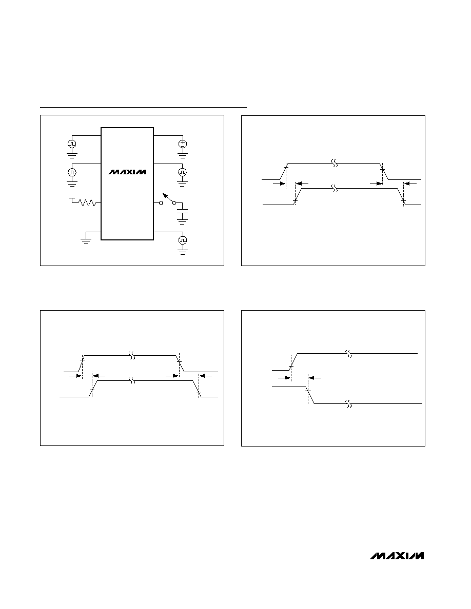
ON Low-to-GATE Low
Propagation Delay
t
PHLON
C
GATE
= 0, Figures 1, 2
6
µs
ON High-to-GATE High
Propagation Delay
t
PLHON
C
GATE
= 0, Figures 1, 2
1.7
µs
FB Low-to-PWRGD Low
Propagation Delay
t
PHLFB
Figures 1, 3
3.2
µs
FB High-to-PWRGD High
Propagation Delay
t
PLHFB
Figures 1, 3
1.5
µs
(V
CC
- V
SENSE
) High-to-GATE
Low Propagation Delay
t
PHLSENSE
T
A
= +25°C, C
GATE
= 0, Figures 1, 4
0.5
2
µs
MAX5933AMAX5933F/MAX5947A/B/C
Positive High-Voltage, Hot-Swap Controllers
4
_______________________________________________________________________________________
Test Circuit and Timing Diagrams
MAX5933_
MAX5947_
ON
V
CC
24V
SENSE
GATE
TIMER
FB
PWRGD
GND
5k
V+ = 5V
10nF
Figure 1. Test Circuit
ON
GATE
1.313V
1.233V
5V
1V
t
PHLON
t
PLHON
Figure 2. ON to GATE Timing
FB
PWRGD
1.313V
1V
1.233V
1V
t
PLHFB
t
PHLFB
Figure 3. FB to PWRGD Timing
V
CC
- SENSE
GATE
47mV
V
CC
t
PHLSENSE
Figure 4. SENSE to GATE Timing
MAX5933AMAX5933F/MAX5947A/B/C
Positive High-Voltage, Hot-Swap Controllers
_______________________________________________________________________________________
5
I
CC
vs. V
CC
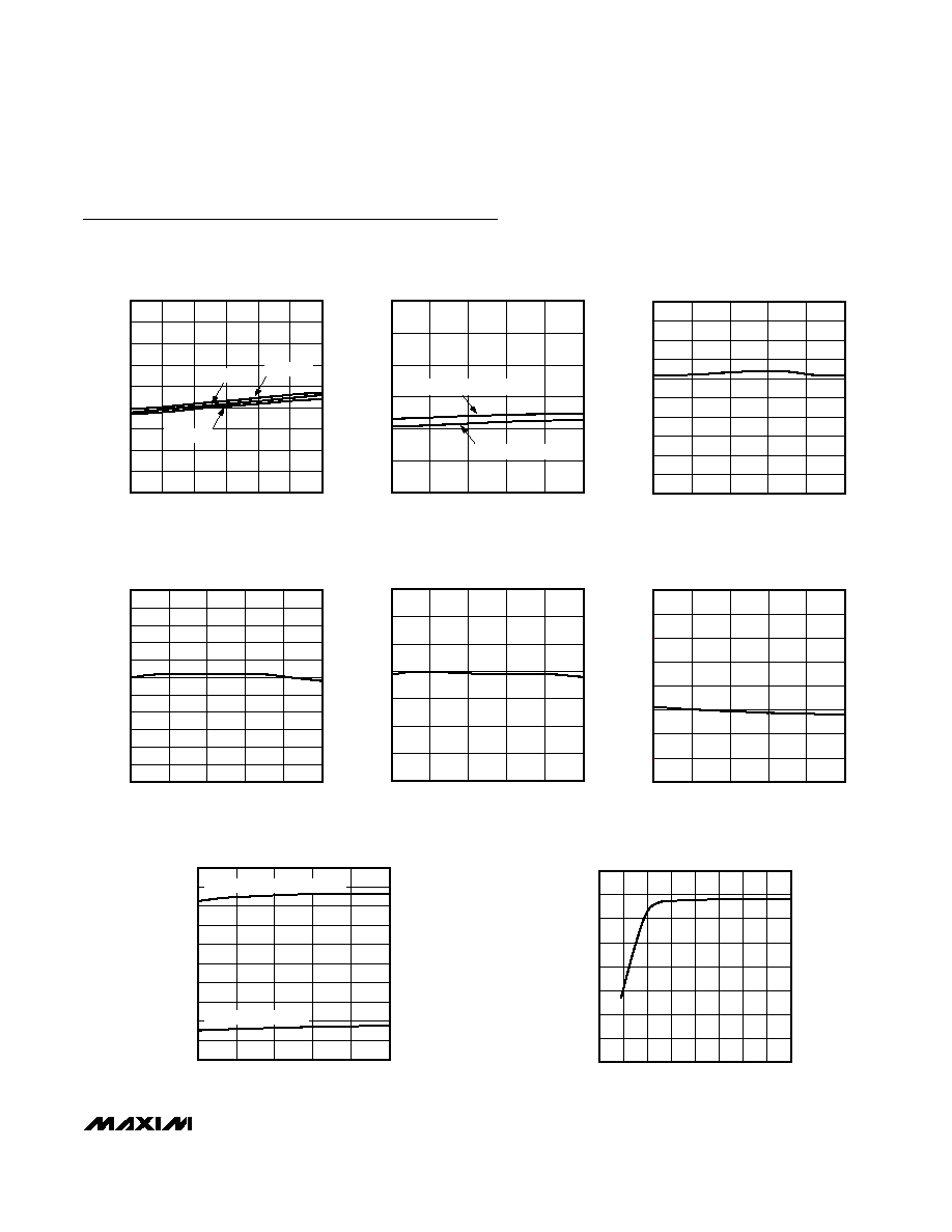
MAX5933 toc01
V
CC
(V)
I
CC
(mA)
0.3
0.6
0.9
1.2
1.5
1.8
2.1
2.4
2.7
0
72
64
56
48
40
33
80
T
A
= -40
°C
T
A
= +25
°C
T
A
= +85
°C
I
CC
vs. TEMPERATURE
MAX5933 toc02
TEMPERATURE (
°C)
I
CC
(mA)
60
35
10
-15
0.5
1.0
1.5
2.0
2.5
3.0
0
-40
85
V
CC
= 48V (MAX5933_/MAX5947_)
V
CC
= 24V (MAX5947_)
FB LOW-VOLTAGE THRESHOLD
vs. TEMPERATURE
MAX5933 toc03
TEMPERATURE (
°C)
FB LOW-VOLTAGE THRESHOLD (V)
60
35
10
-15
1.205
1.210
1.215
1.220
1.225
1.230
1.235
1.240
1.245
1.250
1.200
-40
85
FB HIGH-VOLTAGE THRESHOLD
vs. TEMPERATURE
MAX5933 toc04
TEMPERATURE (
°C)
FB HIGH-VOLTAGE THRESHOLD (V)
60
35
10
-15
-40
85
1.285
1.290
1.295
1.300
1.305
1.310
1.315
1.320
1.325
1.330
1.335
1.280
FB HYSTERESIS vs. TEMPERATURE
MAX5933 toc05
TEMPERATURE (
°C)
FB HYSTERESIS (V)
60
35
10
-15
0.05
0.06
0.07
0.08
0.09
0.10
0.11
0.04
-40
85
I
GATE
PULLUP CURRENT
vs. TEMPERATURE
MAX5933 toc06
TEMPERATURE (
°C)
I
GATE
PULLUP CURRENT (
µ
A)
60
35
-15
10
-12
-11
-10
-9
-7
-8
-6
-5
-13
-40
85
MAX5947_
GATE DRIVE vs. V
CC
MAX5933 toc08
V
CC
(V)
GATE DRIVE (V
GATE
- V
CC
) (V)
60
50
70
40
20
30
10
2
4
6
8
10
12
14
16
0
0
80
GATE DRIVE vs. TEMPERATURE
MAX5933 toc07
TEMPERATURE (
°C)
GATE DRIVE (V
GATE
- V
CC
) (V)
60
35
10
-15
6
7
8
9
10
11
12
13
14
15
5
-40
85
V
CC
= 48V (MAX5933_/MAX5947_)
V
CC
= 10.8V (MAX5947_)
Typical Operating Characteristics
(V
CC
= +48V, T
A
= +25°C, unless otherwise noted.)