 | –≠–ª–µ–∫—Ç—Ä–æ–Ω–Ω—ã–π –∫–æ–º–ø–æ–Ω–µ–Ω—Ç: MAX6101 | –°–∫–∞—á–∞—Ç—å:  PDF PDF  ZIP ZIP |

General Description
The MAX6101≠MAX6105 are low-cost, low-dropout
(LDO), micropower voltage references. These three-termi-
nal references operate with an input voltage range from
(V
OUT
+ 200mV) to 12.6V and are available with output
voltage options of 1.25V, 2.5V, 3V, 4.096V, and 5V. They
feature a proprietary curvature-correction circuit and
laser-trimmed thin-film resistors that result in a low tem-
perature coefficient of 75ppm/∞C (max) and an initial
accuracy of ±0.4% (max). These devices are specified
over the extended temperature range (-40∞C to +85∞C).
These series-mode voltage references draw only 90µA of
supply current and can source 5mA and sink 2mA of load
current. Unlike conventional shunt-mode (two-terminal)
references that waste supply current and require an
external resistor, these devices offer a supply current that
is virtually independent of the supply voltage (with only a
4µA/V variation with supply voltage) and do not require an
external resistor. Additionally, these internally compensat-
ed devices do not require an external compensation
capacitor and are stable with up to 1µF of load capaci-
tance. Eliminating the external compensation capacitor
saves valuable board area in space-critical applications.
Their LDO voltage and supply-independent, ultra-low
supply current make these devices ideal for battery-oper-
ated, high-performance, low-voltage systems.
The MAX6101≠MAX6105 are available in tiny 3-pin
SOT23 packages.
Applications
Portable Battery-Powered Systems
Notebook Computers
PDAs, GPSs, DMMs
Cellular Phones
Hard-Disk Drives
Features
o Ultra-Small 3-Pin SOT23 Package
o Low Cost
o Stable with C
LOAD
= 0 to 1µF
o 5mA Source Current
o ±0.4% max Initial Accuracy
o Low 75ppm/∞C Temperature Coefficient
o 150µA max Quiescent Supply Current
o 50mV Dropout at 1mA Load Current
MAX6101≠MAX6105
Low-Cost, Micropower, Low-Dropout,
High-Output-Current, SOT23 Voltage References
________________________________________________________________ Maxim Integrated Products
1
OUT
1
3
GND
IN
MAX6101
MAX6102
MAX6103
MAX6104
MAX6105
SOT23-3
TOP VIEW
2
19-1613; Rev 0; 1/00
Pin Configuration
Ordering Information
Selector Guide
PART
MAX6101EUR-T
MAX6102EUR-T
MAX6103EUR-T
-40∞C to +85∞C
-40∞C to +85∞C
-40∞C to +85∞C
TEMP. RANGE
PIN-
PACKAGE
3 SOT23-3
3 SOT23-3
3 SOT23-3
TOP
MARK
FZGT
FZGU
FZGV
MAX6104EUR-T
MAX6105EUR-T
-40∞C to +85∞C
-40∞C to +85∞C
3 SOT23-3
3 SOT23-3
FZGW
FZGX
PART
MAX6101
MAX6102
MAX6103
3.000
2.500
1.250
OUTPUT
VOLTAGE (V)
INPUT VOLTAGE
RANGE (V)
2.5 to 12.6
(V
OUT
+ 200mV) to 12.6
(V
OUT
+ 200mV) to 12.6
MAX6104
MAX6105
5.000
4.096
(V
OUT
+ 200mV) to 12.6
(V
OUT
+ 200mV) to 12.6
Note: There is a minimum order increment of 2500 pieces for
SOT packages.
IN
+SUPPLY INPUT (SEE SELECTOR GUIDE)
OUT
REFERENCE
OUT
1
µF MAX*
*CAPACITORS ARE OPTIONAL.
GND
MAX6101
MAX6102
MAX6103
MAX6104
MAX6105
*
Typical Operating Circuit
For free samples and the latest literature, visit www.maxim-ic.com or phone 1-800-998-8800.
For small orders, phone 1-800-835-8769.

MAX6101≠MAX6105
Low-Cost, Micropower, Low-Dropout,
High-Output-Current, SOT23 Voltage References
2
_______________________________________________________________________________________
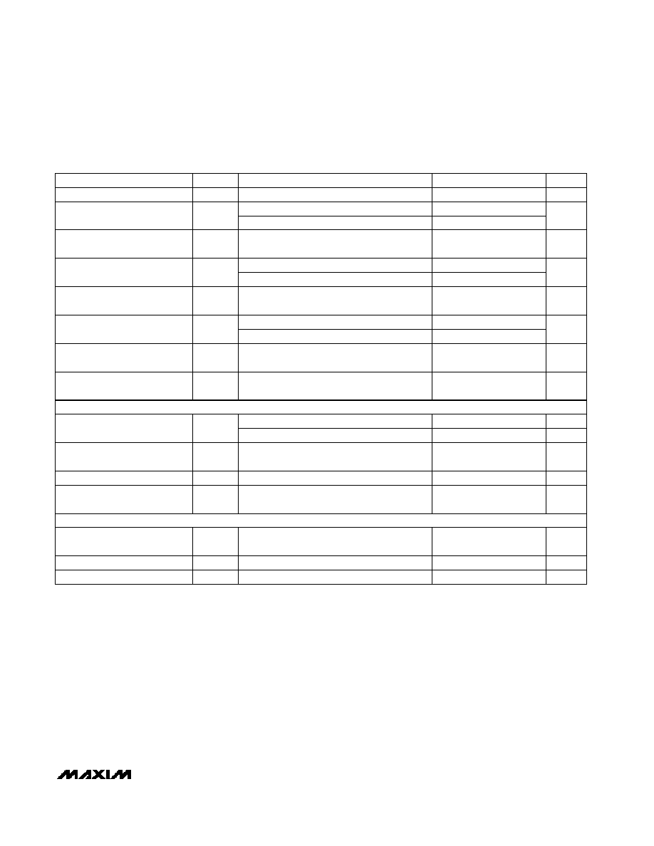
ABSOLUTE MAXIMUM RATINGS
ELECTRICAL CHARACTERISTICS--MAX6101, V
OUT
= 1.25V
(V
IN
= +5V, I
OUT
= 0, T
A
= T
MIN
to T
MAX
, unless otherwise noted. Typical values are at T
A
= +25∞C.) (Note 1)
Stresses beyond those listed under "Absolute Maximum Ratings" may cause permanent damage to the device. These are stress ratings only, and functional
operation of the device at these or any other conditions beyond those indicated in the operational sections of the specifications is not implied. Exposure to
absolute maximum rating conditions for extended periods may affect device reliability.
(Voltages Referenced to GND)
IN .........................................................................-0.3V to +13.5V
OUT .............................................................-0.3V to (V
IN
+ 0.3V)
Output Short Circuit to GND or IN (V
IN
< 6V) ............Continuous
Output Short Circuit to GND or IN (V
IN
6V) .........................60s
Continuous Power Dissipation (T
A
= +70∞C)
3-Pin SOT23 (derate 4.0mW/∞C above +70∞C)............320mW
Operating Temperature Range ...........................-40∞C to +85∞C
Storage Temperature Range .............................-65∞C to +150∞C
Lead Temperature (soldering, 10s) .................................+300∞C
-40∞C to +85∞C
2.5V
V
IN
12.6V
0∞C to +70∞C
T
A
= +25∞C
Guaranteed by line-regulation test
To V
OUT
= 0.1% of final value, C
OUT
= 50pF
V
IN
= 5V ±100mV, f = 120Hz
1000h at +25∞C
Short to IN
2.5V
V
IN
12.6V
Sourcing: 0
I
OUT
4mA
Sinking: -2mA
I
OUT
0
f = 10Hz to 10kHz
Short to GND
f = 0.1Hz to 10Hz
CONDITIONS
µA/V
4
10
I
IN
/V
IN
Change in Supply Current
µA
90
150
I
IN
Quiescent Supply Current
V
2.5
12.6
V
IN
Supply Voltage Range
µF
0
1.0
C
OUT
Capacitive-Load Stability Range
(Note 3)
µs
50
t
R
Turn-On Settling Time
dB
86
V
OUT
/
V
IN
Ripple Rejection
µV
RMS
15
µVp-p
13
e
OUT
Noise Voltage
75
ppm/∞C
65
TCV
OUT
V
1.245
1.250
1.255
V
OUT
Output Voltage
Output Voltage Temperature
Coefficient (Notes 2, 3)
ppm
130
V
OUT
/
cycle
Output Voltage Hysteresis
(Note 4)
ppm/
1000h
50
V
OUT
/
time
Long-Term Stability
25
µV/V
7
90
V
OUT
/
V
IN
Line Regulation
mV/mA
0.7
0.9
V
OUT
/
I
OUT
Load Regulation
0.03
3.0
mA
25
I
SC
OUT Short-Circuit Current
UNITS
MIN
TYP
MAX
SYMBOL
PARAMETER
DYNAMIC CHARACTERISTICS
INPUT CHARACTERISTICS
MAX6101≠MAX6105
Low-Cost, Micropower, Low-Dropout,
High-Output-Current, SOT23 Voltage References
_______________________________________________________________________________________
3
ELECTRICAL CHARACTERISTICS--MAX6102, V
OUT
= 2.50V
(V
IN
= +5V, I
OUT
= 0, T
A
= T
MIN
to T
MAX
, unless otherwise noted. Typical values are at T
A
= +25∞C.) (Note 1)
-40∞C to +85∞C
(V
OUT
+ 0.2V)
V
IN
12.6V
0∞C to +70∞C
T
A
= +25∞C
Guaranteed by line-regulation test
(Note 2)
To V
OUT
= 0.1% of final value, C
OUT
= 50pF
V
IN
= 5V ±100mV, f = 120Hz
1000h at +25∞C
Short to IN
(V
OUT
+ 0.2V)
V
IN
12.6V
Sourcing: 0
I
OUT
5mA
Sinking: -2mA
I
OUT
0
f = 10Hz to 10kHz
Short to GND
f = 0.1Hz to 10Hz
CONDITIONS
µA/V
4
10
I
IN
/V
IN
Change in Supply Current
µA
90
150
I
IN
Quiescent Supply Current
V
V
OUT
+
12.6
0.2
V
IN
Supply Voltage Range
µF
0
1.0
C
OUT
Capacitive-Load Stability Range
(Note 3)
µs
115
t
R
Turn-On Settling Time
dB
86
V
OUT
/
V
IN
Ripple Rejection
µV
RMS
30
µVp-p
27
e
OUT
Noise Voltage
75
ppm/∞C
65
TCV
OUT
V
2.490
2.50
2.510
V
OUT
Output Voltage
Output Voltage Temperature
Coefficient (Notes 2, 3)
ppm
130
V
OUT
/
cycle
Output Voltage Hysteresis
(Note 4)
ppm/
1000h
50
V
OUT
/
time
Long-Term Stability
25
µV/V
12
300
V
OUT
/
V
IN
Line Regulation
mV/mA
0.6
0.9
V
OUT
/
I
OUT
Load Regulation
0.025
6.0
mA
25
I
SC
OUT Short-Circuit Current
UNITS
MIN
TYP
MAX
SYMBOL
PARAMETER
I
OUT
= 1mA
mV
50
200
V
IN
-
V
OUT
Dropout Voltage (Note 5)
DYNAMIC CHARACTERISTICS
INPUT CHARACTERISTICS

MAX6101≠MAX6105
Low-Cost, Micropower, Low-Dropout,
High-Output-Current, SOT23 Voltage References
4
_______________________________________________________________________________________
ELECTRICAL CHARACTERISTICS--MAX6103, V
OUT
= 3.0V
(V
IN
= +5V, I
OUT
= 0, T
A
= T
MIN
to T
MAX
, unless otherwise noted. Typical values are at T
A
= +25∞C.) (Note 1)
I
OUT
= 1mA
mV
-40∞C to +85∞C
50
200
(V
OUT
+ 0.2V)
V
IN
12.6V
0∞C to +70∞C
T
A
= +25∞C
Guaranteed by line-regulation test
To V
OUT
= 0.1% of final value, C
OUT
= 50pF
V
IN
= 5V ±100mV, f = 120Hz
1000h at +25∞C
Short to IN
(V
OUT
+ 0.2V)
V
IN
12.6V
Sourcing: 0
I
OUT
5mA
Sinking: -2mA
I
OUT
0
f = 10Hz to 10kHz
Short to GND
f = 0.1Hz to 10Hz
CONDITIONS
V
IN
-
V
OUT
Dropout Voltage (Note 5)
µA/V
4
10
I
IN
/V
IN
Change in Supply Current
µA
90
150
I
IN
Quiescent Supply Current
V
V
OUT
+
12.6
0.2
V
IN
Supply Voltage Range
µF
0
1.0
C
OUT
Capacitive-Load Stability Range
(Note 3)
µs
115
t
R
Turn-On Settling Time
dB
76
V
OUT
/
V
IN
Ripple Rejection
µV
RMS
40
µVp-p
35
e
OUT
Noise Voltage
75
ppm/∞C
65
TCV
OUT
V
2.988
3.000
3.012
V
OUT
Output Voltage
Output Voltage Temperature
Coefficient (Notes 2, 3)
ppm
130
V
OUT
/
cycle
Output Voltage Hysteresis
(Note 4)
ppm/
1000h
50
V
OUT
/
time
Long-Term Stability
25
µV/V
13
400
V
OUT
/
V
IN
Line Regulation
mV/mA
0.5
0.9
V
OUT
/
I
OUT
Load Regulation
0.018
7.0
mA
25
I
SC
OUT Short-Circuit Current
UNITS
MIN
TYP
MAX
SYMBOL
PARAMETER
DYNAMIC CHARACTERISTICS
INPUT CHARACTERISTICS

MAX6101≠MAX6105
Low-Cost, Micropower, Low-Dropout,
High-Output-Current, SOT23 Voltage References
_______________________________________________________________________________________
5
ELECTRICAL CHARACTERISTICS--MAX6104, V
OUT
= 4.096V
(V
IN
= +5V, I
OUT
= 0, T
A
= T
MIN
to T
MAX
, unless otherwise noted. Typical values are at T
A
= +25∞C.) (Note 1)
I
OUT
= 1mA
mV
-40∞C to +85∞C
50
200
(V
OUT
+ 0.2V)
V
IN
12.6V
0∞C to +70∞C
T
A
= +25∞C
Guaranteed by line-regulation test
To V
OUT
= 0.1% of final value, C
OUT
= 50pF
V
IN
= 5V ±100mV, f = 120Hz
1000h at +25∞C
Short to IN
(V
OUT
+ 0.2V)
V
IN
12.6V
Sourcing: 0
I
OUT
5mA
Sinking: -2mA
I
OUT
0
f = 10Hz to 10kHz
Short to GND
f = 0.1Hz to 10Hz
CONDITIONS
V
IN
-
V
OUT
Dropout Voltage (Note 5)
µA/V
4
10
I
IN
/V
IN
Change in Supply Current
µA
90
150
I
IN
Quiescent Supply Current
V
V
OUT
+
12.6
0.2
V
IN
Supply Voltage Range
µF
0
1.0
C
OUT
Capacitive-Load Stability Range
(Note 3)
µs
190
t
R
Turn-On Settling Time
dB
72
V
OUT
/
V
IN
Ripple Rejection
µV
RMS
50
µVp-p
50
e
OUT
Noise Voltage
75
ppm/∞C
65
TCV
OUT
V
4.080
4.096
4.112
V
OUT
Output Voltage
Output Voltage Temperature
Coefficient (Notes 2, 3)
ppm
130
V
OUT
/
cycle
Output Voltage Hysteresis
(Note 4)
ppm/
1000h
50
V
OUT
/
time
Long-Term Stability
25
µV/V
20
430
V
OUT
/
V
IN
Line Regulation
mV/mA
0.5
0.9
V
OUT
/
I
OUT
Load Regulation
0.018
8
mA
25
I
SC
OUT Short-Circuit Current
UNITS
MIN
TYP
MAX
SYMBOL
PARAMETER
DYNAMIC CHARACTERISTICS
INPUT CHARACTERISTICS