 | –≠–ª–µ–∫—Ç—Ä–æ–Ω–Ω—ã–π –∫–æ–º–ø–æ–Ω–µ–Ω—Ç: MAX613 | –°–∫–∞—á–∞—Ç—å:  PDF PDF  ZIP ZIP |
_______________General Description
The MAX613/MAX614 contain switches for the VPP
supply-voltage lines for Personal Computer Memory
Card International Association (PCMCIA) Release 2.0
card slots. These ICs also contain level-translator out-
puts to switch the PCMCIA card VCC.
The MAX613 allows digital control of two separate VPP
lines that can be switched between 0V, VCC, +12V,
and high impedance. It also includes level shifters that
allow the control of N-channel power MOSFETs for con-
necting and disconnecting the slot VCC supply voltage.
The MAX614 controls a single VPP supply-voltage line
and includes one level shifter in an 8-pin package.
________________________Applications
Notebook and Palmtop Computers
Personal Organizers
Digital Cameras
Handiterminals
Bar-Code Readers
____________________________Features
o
Logic Compatible with Industry-Standard PCMCIA
Digital Controllers:
Intel 82365SL
Intel 82365SL DF
Vadem VG-365
Vadem VG-465
Vadem VG-468
Cirrus Logic CL-PD6710
Cirrus Logic CL-PD6720
o
0V/VCC/+12V/High-Impedance VPP Outputs
o
Internal 1.6
VPP Power Switches
o
10
m
A Quiescent Supply Current
o
Break-Before-Make Switching
o
VCC Switch Control
______________Ordering Information
MAX613/MAX614
Dual-Slot PCMCIA
Analog Power Controllers
________________________________________________________________
Maxim Integrated Products
1
1
2
3
4
5
6
7
GND
AVPP1
AVPP0
BVPP1
BVPP0
VCC1
VCC0
TOP VIEW
MAX613
DIP/SO
VPPIN
VCCIN
AVPP
BVPP
SHDN
DRV3
DRV5
14
13
12
11
10
9
8
1
2
3
4
GND
AVPP1
AVPP0
VCC0
MAX614
DIP/SO
VPPIN
VCCIN
AVPP
DRV
8
7
6
5
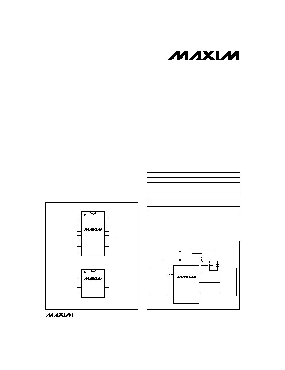
_________________Pin Configurations
PC CARD
SOCKET
CONTROLLER
MAX613
VCCIN
VPPIN
DRV3
AVPP
BVPP
+12V
VCC
VPP1
VPP2
VCC
PCMCIA
SLOT
+5V
5
_________Typical Operating Circuit
Call toll free 1-800-998-8800 for free samples or literature.
19-0188; Rev 0; 11/93
PART
TEMP. RANGE
PIN-PACKAGE
MAX613
CPD
0∞C to +70∞C
14 Plastic DIP
MAX613CSD
0∞C to +70∞C
14 SO
MAX613EPD
-40∞C to +85∞C
14 Plastic DIP
MAX613ESD
-40∞C to +85∞C
14 SO
MAX614
CPA
0∞C to +70∞C
8 Plastic DIP
MAX614CSA
0∞C to +70∞C
8 SO
MAX614EPA
-40∞C to +85∞C
8 Plastic DIP
MAX614ESA
-40∞C to +85∞C
8 SO
MAX613/MAX614
Dual-Slot PCMCIA
Analog Power Controllers
2
_______________________________________________________________________________________
ABSOLUTE MAXIMUM RATINGS
ELECTRICAL CHARACTERISTICS
(VCCIN = +5V, VPPIN = +12V, T
A
= T
MIN
to T
MAX
, unless otherwise noted.)
Stresses beyond those listed under "Absolute Maximum Ratings" may cause permanent damage to the device. These are stress ratings only, and functional
operation of the device at these or any other conditions beyond those indicated in the operational sections of the specifications is not implied. Exposure to
absolute maximum rating conditions for extended periods may affect device reliability.
VCCIN to GND.............................................................+7V, -0.3V
VPPIN to GND ........................................................+13.2V, -0.3V
DRV5, DRV3, DRV to GND ........................(VPPIN + 0.3V), -0.3V
AVPP, BVPP to GND ..................................(VPPIN + 0.3V), -0.3V
All Other Pins to GND ...............................(VCCIN + 0.3V), -0.3V
Continuous Power Dissipation (T
A
= +70∞C)
8-Pin Plastic DIP (derate 9.09mW/∞C above +70∞C) ....727mW
8-Pin SO (derate 5.88mW/∞C above +70∞C).......................471mW
14-Pin Plastic DIP (derate 10.00mW/∞C above +70∞C).......800mW
14-Pin SO (derate 8.33mW/∞C above +70∞C) ..............667mW
Operating Temperature Ranges:
MAX61_C__ ........................................................0∞C to +70∞C
MAX61_E__ .....................................................-40∞C to +85∞C
Storage Temperature Range .............................-65∞C to +160∞C
Lead Temperature (soldering, 10sec) .............................+300∞C
PARAMETER
VCCIN Supply Current
(12V Mode)
MIN
TYP
MAX
AVPP = BVPP = VPPIN
3.5
UNITS
µ
A
2
VPPIN Supply Current
(5V Mode)
20
VPPIN = 12.6V,
AVPP = BVPP= VCCIN
0.05
µ
A
0.05
1
2.25
10
0.05
VPPIN Supply Current
(0V Mode)
AVPP = BVPP = 0V
0.05
µ
A
3.5
VCCIN Supply Current
(5V Mode)
AVPP = BVPP = VCCIN
2.25
3.5
10
µ
A
0.05
22
50
VPPIN Input Voltage Range
3.5
10
VCCIN Supply Current
(0V Mode)
AVPP = BVPP = 0V
VCCIN Input Voltage Range
3.5
2.85
5.5
µ
A
V
20
0
12.6
V
3.5
VPPIN Supply Current
(12V Mode)
AVPP = BVPP = VPPIN =12.6V
0.05
1
CONDITIONS
≠
S
--
H
--
D
--
N = 0V
≠
S
--
H
--
D
--
N = VCCIN
≠
S
--
H
--
D
--
N = 0V
≠
S
--
H
--
D
--
N = 0V
≠
S
--
H
--
D
--
N = VCCIN
≠
S
--
H
--
D
--
N = VCCIN
≠
S
--
H
--
D
--
N = 0V
≠
S
--
H
--
D
--
N = VCCIN
µ
A
≠
S
--
H
--
D
--
N = VCCIN
≠
S
--
H
--
D
--
N = VCCIN
≠
S
--
H
--
D
--
N = 0V
≠
S
--
H
--
D
--
N = 0V
MAX614
MAX614
MAX613
MAX613
MAX613
MAX613
MAX614
MAX613
MAX614
MAX614
MAX613
MAX614
POWER REQUIREMENTS
MAX613/MAX614
Dual-Slot PCMCIA
Analog Power Controllers
_______________________________________________________________________________________
3
ELECTRICAL CHARACTERISTICS (continued)
(VCCIN = +5V, VPPIN = +12V, T
A
= T
MIN
to T
MAX
, unless otherwise noted.)
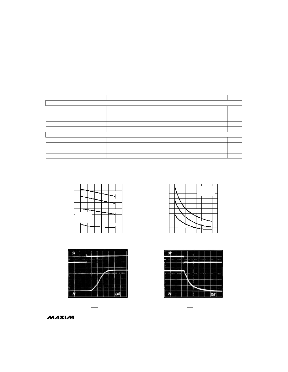
AVPP SWITCH RESISTANCE
(12V MODE)
SWITCH RESISTANCE (
)
1.0
10.0
VPPIN (V)
MAX931-24-01
1.4
1.8
2.2
2.6
10.5
11.0
11.5
12.0
12.5
13.0
13.5
+125∞C
+85∞C
+25∞C
-55∞C
VCCIN = +5.0V
AVPP0 = 0V
AVPP1 = +5.0V
AVPP SWITCH RESISTANCE
(5V MODE)
SWITCH
RESISTANCE
(
)
10
2.0
VCCIN (V)
MAX613/14-02
2.5 3.0 3.5 4.0 4.5 5.0 5.5 6.0 6.5
30
50
70
90
110
VPPIN = +12.0V
AVPP1 = 0V
AVPP0 = VCCIN
+125∞C
+25∞C
-55∞C
__________________________________________Typical Operating Characteristics
(Circuit of Figure 1, T
A
= +25∞C, unless otherwise noted.)
PARAMETER
CONDITIONS
MIN
TYP
MAX
AVPP, BVPP Switch Resistance
VPPIN = 11.4V, 0mA < I
LOAD
< 120mA (12V mode)
1.60
2.45
VCCIN = 4.5V, 0mA < I
LOAD
< 1mA (5V mode)
30
50
VPPIN = 11.4V, 0mA < I
LOAD
< 1mA (0V mode)
135
300
DRV, DRV3, DRV5 Leakage Current
High-impedance mode
1
75
nA
DRV, DRV3, DRV5 Output Voltage Low
I
LOAD
= 1mA
0.1
0.4
V
Logic Input Leakage Current
1
µ
A
Logic Input High
2.4
V
Logic Input Low
0.8
V
_VCC_ to DRV_ Propagation Delay
50
ns
C
VPPIN
= 1
µ
F, AVPP0 = AVPP1, C
AVPP
= 0.1
µ
F
AVPP SWITCHING 5V TO 12V
+5V
AVPP1
+5V
1
µ
s/div
0V
+12V
AVPP
C
VPPIN
= 1
µ
F, AVPP0 = AVPP1, C
AVPP
= 0.1
µ
F
AVPP SWITCHING 12V TO 5V
+5V
AVPP1
+5V
2
µ
s/div
0V
+12V
AVPP
UNITS
DC CHARACTERISTICS
LOGIC SECTION

_______________Detailed Description
VPP Switching
The MAX613/MAX614 allow simple switching of
PCMCIA card VPP to 0V, +5V, and +12V. On-chip
power MOSFETs connect AVPP and BVPP to either
GND, VCCIN, or VPPIN. The AVPP0 and AVPP1 control
logic inputs determine AVPP's state. Likewise, BVPP0
and BVPP1 control BVPP. AVPP and BVPP can also be
programmed to be high impedance.
Each PCMCIA card slot has two VPP voltage inputs
labeled VPP1 and VPP2. Typically, VPP1 supplies the
flash chips that store the low-order byte of the 16-bit
words, and VPP2 supplies the chips that contain the
high-order byte. Programming the high-order bytes
separately from the low-order bytes may be necessary
to minimize +12V current consumption. A single 8-bit
flash chip typically requires at most 30mA of +12V VPP
current during erase or programming.
Thus, systems with less than 60mA current capability
from +12V cannot program two 8-bit flash chips simulta-
neously, and need separate controls for VPP1 and VPP2.
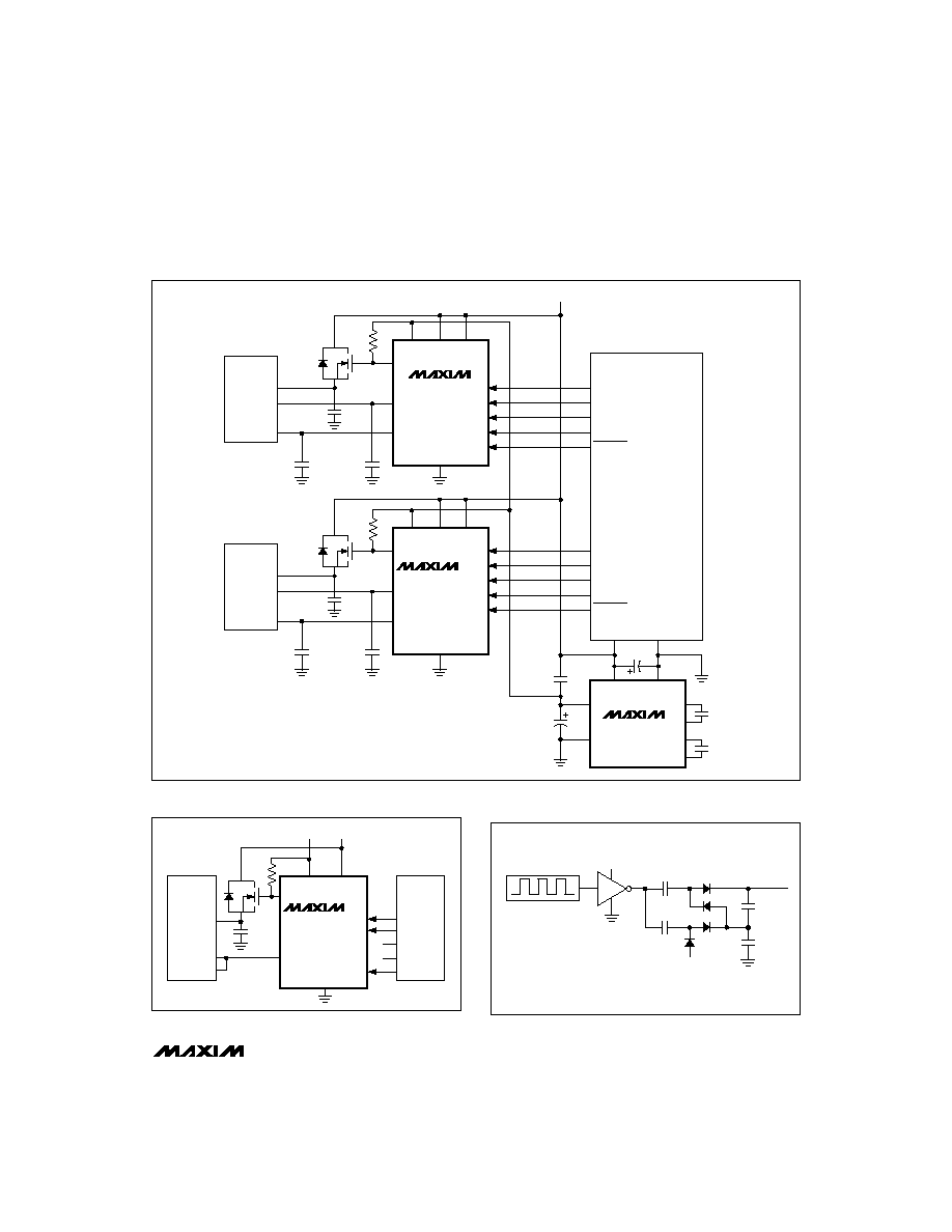
Figure 1 shows an example of a power-control circuit
using the MAX613 to control VPP1 and VPP2 separately.
Figure 1's circuit uses a MAX662 charge-pump DC-DC
converter to convert +5V to +12V at 30mA output current
capability without an inductor. When higher VPP cur-
rent is required, the MAX734 can supply 120mA.
Use the MAX614 for single-slot applications that do
not require a separate VPP1 and VPP2. Figure 2
shows the MAX614 interfaced to the Vadem VG-465
single-slot controller.
To prevent VPP overshoot resulting from parasitic
inductance in the +12V supply, the VPPIN bypass
capacitor's value must be at least 10 times greater than
the capacitance from AVPP or BVPP to GND; the AVPP
and BVPP bypass capacitors must be at least 0.01
µ
F.
______________________________________________________________Pin Description
MAX613/MAX614
Dual-Slot PCMCIA
Analog Power Controllers
4
_______________________________________________________________________________________
PIN
MAX613
14
8
VPPIN
1
1
GND
Ground
2
2
AVPP1
Logic inputs that control the voltage on AVPP (see Table 1 in
Detailed Description).
3
3
AVPP0
4
--
BVPP1
Logic inputs that control the voltage on BVPP (see Table 2 in
Detailed Description).
5
--
BVPP0
6
--
VCC1
Logic input that controls the state of DRV3 and DRV5 (see Table 3 in
Detailed Description).
7
4
VCC0
Logic input that controls the state of DRV on the MAX614. On the MAX613, both VCC0 and
VCC1 control the state of DRV3 and DRV5 (see Table 3 in
Detailed Description).
--
5
DRV
Open-drain power MOSFET gate-driver output used to switch the slot VCC supply voltage.
DRV sinks current when VCC0 is high and goes high impedance when VCC0 is low.
8
--
DRV5
Open-drain power MOSFET gate-driver output used to switch the slot VCC supply voltage (see
Table 3 in
Detailed Description).
9
--
DRV3
Open-drain power MOSFET gate-driver output used to switch the slot VCC supply voltage (see
Table 3 in
Detailed Description).
10
--
≠
S
--
H
--
D
--
N
Logic-level shutdown input. When
≠
S
--
H
--
D
--
N is low, DRV3 and DRV5 sink current regardless of the state of
VCC0 and VCC1. When
≠
S
--
H
--
D
--
N is high, DRV3 and DRV5 are controlled by VCC0 and VCC1.
11
--
BVPP
Switched output, controlled by BVPP1 and BVPP0, that outputs 0V, +5V, or +12V. BVPP can
also be programmed to go high impedance (see Table 2 in
Detailed Description).
12
6
AVPP
Switched output, controlled by AVPP1 and AVPP0, that outputs 0V, +5V, or +12V. AVPP can
also be programmed to go high impedance (see Table 1 in
Detailed Description).
13
7
VCCIN
+5V power input
+12V power input. VPPIN can have 0V or +5V applied as long as VCCIN > 2.85V.
MAX614
NAME
FUNCTION
MAX613/MAX614
Dual-Slot PCMCIA
Analog Power Controllers
_______________________________________________________________________________________
5
MAX613
VCCIN VCC1
AVPP0
AVPP1
BVPP0
BVPP1
VCC0
VCC
VPP1
VPP2
PCMCIA
SLOT B
VPPIN
DRV3
AVPP
BVPP
GND
1
/
2
Si9956DY
M2
0.1
µ
F
1
µ
F
0.1
µ
F
100k
MAX613
VCCIN VCC1
AVPP0
AVPP1
BVPP0
BVPP1
VCC0
VCC
VPP1
VPP2
PCMCIA
SLOT A
VPPIN
DRV3
AVPP
BVPP
GND
1
/
2
Si9956DY
M1
0.1
µ
F
1
µ
F
0.1
µ
F
100k
MAX662
GND
VCC
VOUT
SHDN
4.7
µ
F
0.1
µ
F
C1+
C1-
C2+
C2-
A: V
PP
1_EN0 (A_VPP1EN0)
A:V
PP
1_EN1 (A_VPP1EN1)
A:V
PP
2_EN0 (A_VPP2EN0)
A:V
PP
2_EN1 (A_VPP2EN1)
A:V
CC
_EN (A_VCCEN)
B:V
PP
1_EN0 (B_VPP1EN0)
B:V
PP
1_EN1 (B_VPP1EN1)
B:V
PP
2_EN0 (B_VPP2EN0)
B:V
PP
2_EN1 (B_VPP2EN1)
B:V
CC
_EN (B_VCCEN)
4.7
µ
F
0.22
µ
F
0.22
µ
F
+5V
INTEL 82365SL
VADEM VG-365
or
VADEM VG-468)
VCC
VSS
100k
Figure 1. MAX613 Dual Slot, Separate VPP1 and VPP2, 5V Only VCC Operating Circuit
0.1
µ
F
9.97V (WITH
100k
LOAD)
10nF
10nF
4.5V MIN
NOTE:
1. ALL DIODES 1N4148.
2. OSCILLATOR FREQUENCY CAN BE
INCREASED FOR HIGHER OUTPUT POWER.
0.1
µ
F
32.76kHz
50% DUTY CYCLE
4.5V MIN
MAX614
VCCIN
AVPP0
AVPP1
VCC0
VCC
VPP1
VPP2
VPPIN
DRV
AVPP
GND
1
µ
F
100k
VPP1EN0
VPP1EN1
VPP2EN0
VPP2EN1
VCCEN
VADEM
VG-465
+5V
+12V
PCMCIA
SLOT
Figure 2. MAX614 Single-Slot Application
Figure 3. Charge Pump