 | –≠–ª–µ–∫—Ç—Ä–æ–Ω–Ω—ã–π –∫–æ–º–ø–æ–Ω–µ–Ω—Ç: MAX619 | –°–∫–∞—á–∞—Ç—å:  PDF PDF  ZIP ZIP |

_______________General Description
The MAX619 step-up charge-pump DC-DC converter
delivers a regulated 5V ±4% output at 50mA over tem-
perature. The input voltage range is 2V to 3.6V (two
battery cells).
The complete MAX619 circuit fits into less than 0.1in
2
of
board space because it requires only four external
capacitors: two 0.22
µ
F flying capacitors, and 10
µ
F
capacitors at the input and output.
Low operating supply current (150
µ
A max) and low
shutdown supply current (1
µ
A max) make this device
ideal for small, portable, and battery-powered applica-
tions. When shut down, the load is disconnected from
the input.
The MAX619 is available in 8-pin DIP and SO packages.
________________________Applications
Two Battery Cells to 5V Conversion
Local 3V-to-5V Conversion
Portable Instruments & Handy-Terminals
Battery-Powered Microprocessor-Based Systems
5V Flash Memory Programmer
Minimum Component DC-DC Converters
Remote Data-Acquisition Systems
Compact 5V Op-Amp Supply
Regulated 5V Supply from Lithium Backup Battery
Switching Drive Voltage for MOSFETs in
Low-Voltage Systems
____________________________Features
o
Regulated 5V ±4% Charge Pump
o
Output Current Guaranteed over Temperature
20mA (V
IN
2V)
50mA (V
IN
3V)
o
2V to 3.6V Input Range
o
No Inductors; Very Low EMI Noise
o
Ultra-Small Application Circuit (0.1in
2
)
o
Uses Small, Inexpensive Capacitors
o
500kHz Internal Oscillator
o
Logic-Controlled 1
µ
A Max Shutdown
Supply Current
o
Shutdown Disconnects Load from Input
o
8-Pin DIP and SO Packages
_______________Ordering Information
* Dice are specified at T
A
= +25 ∞C.
MAX619
Regulated 5V Charge-Pump
DC-DC Converter
________________________________________________________________
Maxim Integrated Products
1
1
2
3
4
8
7
6
5
MAX619
DIP/SO
C1+
IN
OUT
C2+
C1-
SHDN
GND
C2-
TOP VIEW
__________________Pin Configuration
MAX619
OUT
C2+
C2-
IN
SHDN
C1+
C1-
INPUT
2V to 3.6V
ON/OFF
0.22
µ
F
OUTPUT
5V, 20mA
10
µ
F
10
µ
F
0.22
µ
F
GND
__________Typical Operating Circuit
19-0227; Rev 2; 5/96
EVALUATION KIT MANUAL
FOLLOWS DATA SHEET
For free samples & the latest literature: http://www.maxim-ic.com, or phone 1-800-998-8800
PART
TEMP. RANGE
PIN-PACKAGE
MAX619CPA
0∞C to +70∞C
8 Plastic DIP
MAX619CSA
0∞C to +70∞C
8 SO
MAX619C/D
0∞C to +70∞C
Dice*
MAX619EPA
-40∞C to +85∞C
8 Plastic DIP
MAX619ESA
-40∞C to +85∞C
8 SO
MAX619MJA
-55∞C to +125∞C
8 CERDIP

MAX619
Regulated 5V Charge-Pump
DC-DC Converter
2
________________________________________________________________________________________
ABSOLUTE MAXIMUM RATINGS
ELECTRICAL CHARACTERISTICS
(V
IN
= 2V to 3.6V, C1 = C2 = 0.22
µ
F, C3 = C4 = 10µF, T
A
= T
MIN
to T
MAX
, unless otherwise noted. Typical values are at T
A
= +25∞C.)
Note 1:
The MAX619 is not short-circuit protected.
PARAMETER
SYMBOL
MIN
TYP
MAX
UNITS
No-Load Supply Current
75
170
µ
A
0.02
1
Shutdown Supply
Current
10
µ
A
82
Input Voltage
V
IN
2
3.6
V
82
80
Efficiency
Eff
%
Switching Frequency
500
kHz
V
IH
0.7 x V
IN
SHDN Input Threshold
V
IL
0.4
V
±1
SHDN Input Current
I
IH
±10
µ
A
CONDITIONS
V
IN
= 3V, I
OUT
= 30mA
2V
V
IN
3.6V, IOUT = 0mA
V
IN
= 2V, I
OUT
= 20mA
2V
VIN
3.6V, IOUT = 0mA,
VSHDN = VIN
V
IN
= 3V, I
OUT
= 20mA
At full load
V
SHDN
= V
IN
V
IN
to GND ............................................................-0.3V to +5.5V
V
OUT
to GND .........................................................-0.3V to +5.5V
SHDN to GND ..............................................-0.3V to (V
IN
+ 0.3V)
I
OUT
Continuous (Note 1)..................................................120mA
Continuous Power Dissipation (T
A
= +70∞C)
Plastic DIP (derate 9.09mW/∞C above +70∞C) ............727mW
SO (derate 5.88mW/∞C above +70∞C) .........................471mW
CERDIP (derate 8.00mW/∞C above +70∞C) .................640mW
Operating Temperature Ranges
MAX619C_ _ .......................................................0∞C to +70∞C
MAX619E_ _ ....................................................-40∞C to +85∞C
MAX619MJA ..................................................-55∞C to +125∞C
Storage Temperature Range .............................-65∞C to +165∞C
Lead Temperature (soldering, 10sec) .............................+300∞C
MAX619C/E
MAX619M
MAX619C/E
MAX619M
I
IN
2.0V
V
IN
3.6V, 0mA
I
OUT
20mA
3.0V
V
IN
3.6V, 0mA
I
OUT
50mA, MAX619C
3.0V
V
IN
3.6V, 0mA
I
OUT
45mA, MAX619E
Output Ripple
V
RIPPLE
100
mV
No load to full load
Stresses beyond those listed under "Absolute Maximum Ratings" may cause permanent damage to the device. These are stress ratings only, and functional
operation of the device at these or any other conditions beyond those indicated in the operational sections of the specifications is not implied. Exposure to
absolute maximum rating conditions for extended periods may affect device reliability.
3.0V
V
IN
3.6V, 0mA
I
OUT
40mA, MAX619M
Output Voltage
V
OUT
4.8
5.0
5.2
V
MAX619
Regulated 5V Charge-Pump
DC-DC Converter
________________________________________________________________________________________
3
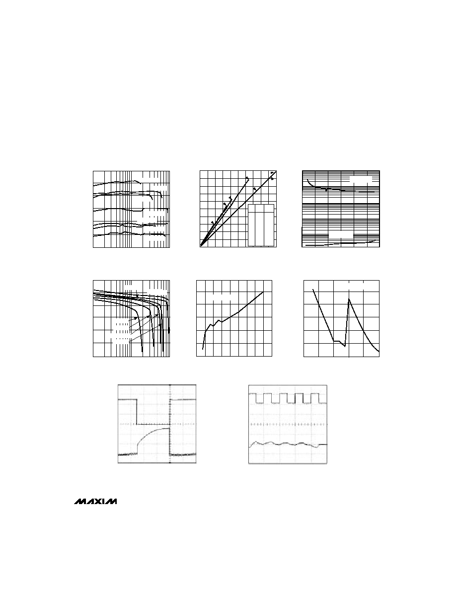
TOP TRACE: OUTPUT CURRENT, 0mA to 25mA, 10mA/div
BOTTOM TRACE: OUTPUT VOLTAGE, 5mV/div, AC-COUPLED
2ms/div
LOAD-TRANSIENT RESPONSE
R
LOAD
= 250
, V
OUT
= 5V, I
OUT
= 20mA
TOP TRACE: V
IN
= 2V to 3V, 1V/div
BOTTOM TRACE: OUTPUT VOLTAGE, 50mV/div, AC-COUPLED
2ms/div
LINE-TRANSIENT RESPONSE (I
OUT
= 20mA)
__________________________________________Typical Operating Characteristics
(T
A
= +25∞C, unless otherwise noted.)
60
1
10
100
EFFICIENCY vs. OUTPUT CURRENT
AND INPUT VOLTAGE
I
OUT
(mA)
EFFICIENCY (%)
65
70
75
80
85
90
V
IN
= 1.8V
V
IN
= 3.0V
V
IN
= 2.0V
V
IN
= 3.3V
V
IN
= 3.6V
V
IN
= 2.4V
V
IN
= 2.7V
0
0
INPUT CURRENT vs. OUTPUT CURRENT
I
OUT
(mA)
I
IN
(mA)
10 20 30 40 50 60 70 80 90 100
20
40
60
80
100
120
140
160
180
200
V
IN
I
OUT
MAX
A
B
C
D
E
F
G
1.8
2.0
2.4
2.7
3.0
3.6
3.3
18
36
41
64
72
94
100
A
B
C
D
E
G
F
NO-LOAD INPUT CURRENT
vs. INPUT VOLTAGE
V
IN
(V)
I
IN
(
µ
A)
1.5
2.0
2.5
3.0
3.5
4.0
4.5
0.01
0.1
1.0
10
100
1000
SHDN = V
IN
SHDN = 0V
4.75
4.80
1
10
100
OUTPUT VOLTAGE vs. OUTPUT CURRENT
I
OUT
(mA)
V
OUT
(V)
4.85
4.90
4.95
5.00
5.05
V
IN
= 1.8V
V
IN
= 2.0V
V
IN
= 3.3V
V
IN
= 2.4V, 2.7V
= 3.6V
V
IN
= 3.6V
V
IN
= 3.0V
OUTPUT VOLTAGE vs. INPUT VOLTAGE
V
IN
(V)
V
OUT
(V)
2.0
1.5
2.5 3.0 3.5 4.0 4.5 5.0 5.5 6.0
4.94
4.96
4.98
5.00
5.02
5.04
5.06
I
OUT
= 20mA
EFFICIENCY vs. INPUT VOLTAGE
V
IN
(V)
EFFICIENCY (%)
1.5
60
65
70
75
80
85
90
I
OUT
= 10mA
2.0
2.5
3.0
3.5
4.0
MAX619
Regulated 5V Charge-Pump
DC-DC Converter
4
________________________________________________________________________________________
_______________Detailed Description
Operating Principle
The MAX619 provides a regulated 5V output from a 2V
to 3.6V (two battery cells) input. Internal charge pumps
and external capacitors generate the 5V output, elimi-
nating the need for inductors. The output voltage is
regulated to 5V ±4% by a pulse-skipping controller that
turns on the charge pump when the output voltage
begins to droop.
To maintain the greatest efficiency over the entire input
voltage range, the MAX619's internal charge pump
operates as a voltage doubler when V
IN
ranges from
3.0V to 3.6V, and as a voltage tripler when V
IN
ranges
from 2.0V to 2.5V. When V
IN
ranges from 2.5V to 3.0V,
_____________________Pin Description
the MAX619 switches between doubler and tripler
mode on alternating cycles, making a 2.5 x V
IN
charge
pump. To further enhance efficiency over the input
range, an internal comparator selects the higher of V
IN
or V
OUT
to run the MAX619's internal circuitry.
Efficiency with V
IN
= 2V and I
OUT
= 20mA is typically
80%.
Figure 1 shows a detailed block diagram of the
MAX619. In tripler mode, when the S1 switches close,
the S2 switches open and capacitors C1 and C2
charge up to V
IN
. On the second half of the cycle, C1
and C2 are connected in series between IN and OUT
when the S1 switches open and the S2 switches close,
as shown in Figure 1. In doubler mode, only C2 is
used.
During one oscillator cycle, energy is transferred from
the input to the charge-pump capacitors, and then
from the charge-pump capacitors to the output capaci-
tor and load. The number of cycles within a given time
frame increases as the load increases or as the input
supply voltage decreases. In the limiting case, the
charge pumps operate continuously, and the oscillator
frequency is nominally 500kHz.
Shutdown Mode
The MAX619 enters low-power shutdown mode when
SHDN is a logic high. SHDN is a CMOS-compatible
input. In shutdown mode, the charge-pump switching
action is halted, OUT is disconnected from IN, and
V
OUT
falls to 0V. Connect SHDN to ground for normal
operation. When V
IN
= 3.6V, V
OUT
typically reaches
5V in 0.5ms under no-load conditions after SHDN goes
low.
FUNCTION
NAME
PIN
Negative Terminal for C1
C1-
8
Active-High CMOS Logic-Level Shutdown Input
SHDN
7
Ground
GND
6
Negative Terminal for C2
C2-
5
Positive Terminal for C2
C2+
4
+5V Output Voltage. V
OUT
= 0V when in
shutdown mode.
OUT
3
Input Supply Voltage
IN
2
Positive Terminal for C1
C1+
1

MAX619
Regulated 5V Charge-Pump
DC-DC Converter
________________________________________________________________________________________
5
C3
10µF
C2
0.22µF
P
P
C1
0.22µF
C2-
C1+
S1D
C1-
S1C
S2C
S2B
S1B
S1A
S2A
IN
SWITCH
CONTROL
BUS
V
IN
/V
OUT
SD
FB
IN
IC
POWER
*
*
GND
SWITCHES SHOWN IN TRIPLER MODE, DISCHARGE CYCLE
CONTROL
LOGIC
10µF
OUT
V
REF
SHDN
C2+
MAX619
C4
Figure 1. Block Diagram