Maxim cannot assume responsibility for use of any circuitry other than circuitry entirely embodied in a Maxim product. No circuit patent licenses are
implied. Maxim reserves the right to change the circuitry and specifications without notice at any time.
8
___________________Maxim Integrated Products, 120 San Gabriel Drive, Sunnyvale, CA 94086 (408) 737-7600
© 1994 Maxim Integrated Products
Printed USA
is a registered trademark of Maxim Integrated Products.
MAX619 EV
Kit
Evaluation Kit Information
_______________General Description
The MAX619 evaluation kit (EV kit) is a 3V to 5V charge-
pump DC-DC converter capable of driving loads up to
50mA. The circuit consists of the SOIC and four surface-
mount capacitors on a single-layer printed circuit board.
_________________________Quick Start
The MAX619 EV Kit is fully assembled and tested.
Follow the steps below to verify board operation.
Do not turn on the power supply until all connec-
tions are completed.
1. Connect a 2V to 3.6V supply to the pad marked VIN.
The ground connects to the GND pad.
2. Connect a voltmeter and load (if any) to the VOUT
pad.
3. Place the shunt on JU1 across the ON side. This
grounds the SHDN pin to enable the device. Moving
the shunt to the OFF side connects SHDN to VIN to
disable the device. Remove the shunt if an external
signal is connected to the SHDN pad.
4. Turn on the power and verify that the output is
5V ±4%.
____________________________Features
o
2.0V to 3.6V Input Range
o
Up to 50mA Output Current
o
1µA Shutdown Current
______________Ordering Information
C2-
GND
MAX619
SHDN
C1-
C2+
V
OUT
C1+
SHDN
C2
0.22
µ
F
C1
0.22
µ
F
C3
10
µ
F
C4
10
µ
F
V
IN
8
5
4
3
2
1
V
IN
V
OUT
2.0V to 3.6V
5V
OFF
ON
JU1
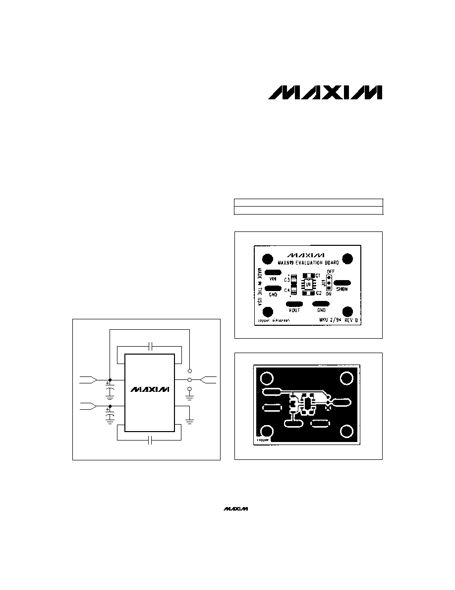
Figure 2. Component Placement Guide--Component Side
Figure 3. PC Board Layout--Component Side
Figure 1. MAX619 EV Kit Schematic
BOARD TYPE
Surface Mount
0∞C to +70∞C
MAX619EVKIT-SO
TEMP. RANGE
PART