 | –≠–ª–µ–∫—Ç—Ä–æ–Ω–Ω—ã–π –∫–æ–º–ø–æ–Ω–µ–Ω—Ç: MAX6312 | –°–∫–∞—á–∞—Ç—å:  PDF PDF  ZIP ZIP |

For free samples & the latest literature: http://www.maxim-ic.com, or phone 1-800-998-8800.
For small orders, phone 408-737-7600 ext. 3468.
General Description
The MAX6305≠MAX6313 CMOS microprocessor (µP)
supervisory circuits are designed to monitor more than
one power supply. Ideal for monitoring both 5V and
3.3V in personal computer systems, these devices
assert a system reset if any of the monitored supplies
falls outside the programmed threshold. Low supply
current (15µA) and a small package suit them for
portable applications. The MAX6305≠MAX6313 are
specifically designed to ignore fast transients on
any monitored supply.
These devices are available in a SOT23-5 package,
have factory-programmed reset thresholds from 2.5V to
5.0V (in 100mV increments), and feature four power-on
reset timeout periods.
Applications
Portable Computers
Computers
Controllers
Intelligent Instruments
Portable/Battery-Powered Equipment
Multivoltage Systems: 3V/5V, 5V/12V, 5V/24V
Embedded Control Systems
Features
o
Small 5-Pin SOT23 Package
o
Precision Factory-Set V
CC
Reset Thresholds;
Available in 0.1V Increments from 2.5V to 5V
o
Immune to Short V
CC
Transients
o
Guaranteed RESET Valid to V
CC
= 1V
o
Guaranteed Over Temperature
o
8µA Supply Current
o
Factory-Set Reset Timeout Delay from
1ms (min) to 1120ms (min)
o
No External Components
o
Manual Reset Input
o
Under/Overvoltage Supply Monitoring
MAX6305≠MAX6313
5-Pin, Multiple-Input,
Programmable Reset ICs
________________________________________________________________
Maxim Integrated Products
1
19-1145; Rev 1; 8/98
PART
MAX6305
UK00D_-T
MAX6306
UK_ _D_-T
MAX6307
UK_ _D_-T
0∞C to +70∞C
0∞C to +70∞C
0∞C to +70∞C
TEMP. RANGE
PIN-PACKAGE
5 SOT23-5
5 SOT23-5
5 SOT23-5
Ordering Information
The MAX6306/MAX6307/MAX6309/MAX6310/MAX6312/
MAX6313 are available with factory-set V
CC
reset thresholds from
2.5V to 5V, in 0.1V increments. Insert the desired nominal reset
threshold (from Table 1) into the blanks following the letters UK.
All parts also offer factory-programmed reset timeout periods.
Insert the number corresponding to the desired nominal timeout
period index following the "D" in the part number (D1 = 1ms min,
D2 = 20ms min, D3 = 140ms min, and D4 = 1120ms min). Contact
factory for availability and minimum order sizes.
Ordering Information continued at end of data sheet.
Pin Configurations and Typical Operating Circuit appear at
end of data sheet.
_______________________________________________________________Selector Table
PART
OPEN-DRAIN
RESET
OUTPUT
PUSH/PULL
RESET
OUTPUT
PUSH/PULL
RESET
OUTPUT
FACTORY-
SET RESET
THRESHOLD
ON V
CC
ADDITIONAL
UNDERVOLTAGE
RESET INPUTS
NEGATIVE/
OVERVOLTAGE
RESET INPUT
MAX6305
--
--
--
2
--
MAX6306
--
--
1
--
MAX6307
--
--
1
MAX6308
--
--
--
2
--
MAX6309
--
--
1
--
MAX6310
--
--
1
MAX6311
--
--
--
2
--
MAX6312
--
--
1
--
MAX6313
--
--
1
MANUAL-
RESET
INPUT
--
--
--
--
--
--

MAX6305≠MAX6313
5-Pin, Multiple-Input,
Programmable Reset ICs
2
_______________________________________________________________________________________
ABSOLUTE MAXIMUM RATINGS
ELECTRICAL CHARACTERISTICS
V
CC
= +2.5V to +5.5V for the MAX6305/MAX6308/MAX6311, V
CC
= (V
TH
+ 2.5%) to +5.5V for the MAX6306/MAX6307/MAX6309/
MAX6310/MAX6312/MAX6313; T
A
= 0∞C to +70∞C; unless otherwise noted. Typical values are at T
A
= +25∞C.)
Stresses beyond those listed under "Absolute Maximum Ratings" may cause permanent damage to the device. These are stress ratings only, and functional
operation of the device at these or any other conditions beyond those indicated in the operational sections of the specifications is not implied. Exposure to
absolute maximum rating conditions for extended periods may affect device reliability.
V
CC
...........................................................................-0.3V to +6V
All Other Pins..............................................-0.3V to (V
CC
+ 0.3V)
Input/Output Current, All Pins .............................................20mA
Rate of Rise, V
CC
............................................................100V/µs
Continuous Power Dissipation (T
A
= +70∞C)
SOT23-5 (derate 7.1mW/∞C above +70∞C).................571mW
Operating Temperature Range...............................0∞C to +70∞C
Storage Temperature Range .............................-65∞C to +160∞C
Lead Temperature (soldering, 10sec) .............................+300∞C
MAX6308/MAX6309/
MAX6310
MAX6305≠MAX6310
MAX6306/MAX6307/
MAX6309/MAX6310/
MAX6312/MAX6313
0.8 x V
CC
0.8 x V
CC
0.3
V
OL
V
0.4
0.8 x V
CC
V
OH
RESET Output
Voltage
V
CC
- 1.5
0.3
V
OL
0.3
0.3
V
0.4
µA
8
16
I
CC
Supply Current
1.0
5.5
V
V
CC
Range
1120
1570
2240
t
RP
Reset Timeout Period
140
200
280
20
28
40
ms
1
1.4
2
V
V
TH
- 1.5%
V
TH
V
TH
+ 1.5%
V
TH
- 2.5%
V
TH
+ 2.5%
V
TH
Reset Threshold
(Note 2)
ppm/∞C
40
V
TH
/∞C
Reset Threshold
Tempco
mV
2 x V
TH
V
TH
HYST
Reset Threshold
Hysteresis
UNITS
MIN
TYP
MAX
SYMBOL
PARAMETER
V
CC
= 5.5V
T
A
= 0∞C to +70∞C,
V
CC
> 1.0V, I
SOURCE
= 10µA
V
CC
> 1.8V,
I
SOURCE
= 150µA
T
A
= 0∞C to +70∞C (Note 1)
V
CC
> 2.5V, I
SINK
= 1.2mA
V
CC
> 4.25V, I
SINK
= 3.2mA
V
CC
> 2.5V,
I
SOURCE
= 500µA
V
CC
> 4.25V,
I
SOURCE
= 800µA
D4
D3
T
A
= 0∞C to +70∞C,
V
CC
> 1.0V, I
SINK
= 50µA
T
A
= 0∞C to +70∞C,
V
CC
> 1.2V, I
SINK
= 500µA
D2
D1
T
A
= +25∞C
T
A
= 0∞C to +70∞C
V
CC
> 2.5V, I
SINK
= 1.2mA
V
CC
> 4.25V, I
SINK
= 3.2mA
CONDITIONS
V
OH
MAX6311/MAX6312/
MAX6313
RESET Output
Voltage

MAX6305≠MAX6313
5-Pin, Multiple-Input,
Programmable Reset ICs
_______________________________________________________________________________________
3
nA
-25
25
I
RST IN_
RST IN Input Current
V
1.20
1.26
V
RSTH
RST IN Input Threshold
1.21
1.23
1.25
µs
1
MR Minimum Input
Pulse
V
0.7 x V
CC
V
IL
MR Input
0.3 x V
CC
2.4
0.8
0V < V
RST IN_
< V
CC
- 0.3V
T
A
= 0∞C to +70∞C
T
A
= +25∞C
UNITS
MIN
TYP
MAX
SYMBOL
PARAMETER
V
TH
< 4.0V
V
TH
> 4.0V
CONDITIONS
ELECTRICAL CHARACTERISTICS (continued)
(V
CC
= +2.5V to +5.5V for the MAX6305/MAX6308/MAX6311, V
CC
= (V
TH
+ 2.5%) to +5.5V for the MAX6306/MAX6307/MAX6309/
MAX6310/MAX6312/MAX6313; T
A
= 0∞C to +70∞C; unless otherwise noted. Typical values are at T
A
= +25∞C.)
RST IN Hysteresis
2.5
mV
V
IL
Note 1:
The MAX6305/MAX6308/MAX6311 switch from undervoltage reset to normal operation between 1.5V < V
CC
< 2.5V.
Note 2:
The MAX6306/MAX6307/MAX6309/MAX6310/MAX6312/MAX6313 monitor V
CC
through an internal factory-trimmed voltage
divider, which programs the nominal reset threshold. Factory-trimmed reset thresholds are available in approximately
100mV increments from 2.5V to 5V (Table 1).
k
32
63.5
100
MR Pull-Up Resistance
nsV
500
MR to Reset Delay
µs
0.1
MR Glitch Rejection
MANUAL-RESET INPUT (MAX6306/MAX6309/MAX6312)
ADJUSTABLE RESET COMPARATOR INPUTS
V
IH
V
IH
MAX6305≠MAX6313
5-Pin, Multiple-Input,
Programmable Reset ICs
4
_______________________________________________________________________________________
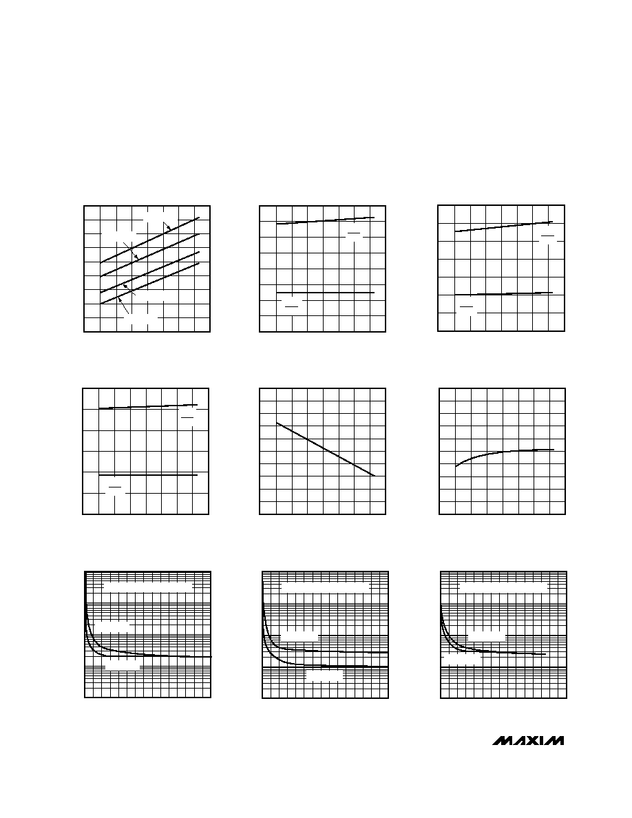
__________________________________________Typical Operating Characteristics
(V
CC
= +5V, T
A
= +25∞C, unless otherwise noted.)
5.0
5.5
6.0
6.5
7.0
7.5
8.0
8.5
9.0
9.5
-60
-40
-20
0
20
40
60
80
100
SUPPLY CURRENT
vs. TEMPERATURE
6305 TOC01
TEMPERATURE (∞C)
SUPPLY CURRENT (
µ
A)
V
CC
= 2.5V
V
CC
= 3.5V
V
CC
= 5.5V
V
CC
= 4.5V
0
10
20
30
40
50
60
70
80
-60
-40
-20
0
20
40
60
80
100
V
CC
FALLING PROPAGATION DELAY
vs. TEMPERATURE
6305 TOC02
TEMPERATURE (∞C)
PROPAGATION DELAY (ns)
1mV
µ
s
10mV
µ
s
0
10
20
30
40
50
60
70
-60
-40
-20
0
20
40
60
80
100
OVRST IN RISING PROPAGATION
DELAY vs. TEMPERATURE
(OVERVOLTAGE RESET INPUT)
6305 TOC03
TEMPERATURE (∞C)
PROPAGATION DELAY (ns)
1mV
µ
s
10mV
µ
s
0
20
40
60
80
100
120
-60
-40
-20
0
20
40
60
80
100
RST IN_ FALLING PROPAGATION
DELAY vs. TEMPERATURE
6305 TOC04
TEMPERATURE (∞C)
RST IN_ PROPAGATION DELAY (ns)
1mV
µ
s
10mV
µ
s
1
0
400
1200
800
MAXIMUM TRANSIENT DURATION vs.
V
CC
RESET THRESHOLD OVERDRIVE
10
6305 TOC7
OVERDRIVE, V
TH
- V
CC
(mV)
TRANSIENT DURATION (
µ
s)
100
1000
10,000
V
TH
= 5.0V
RESET OCCURS ABOVE LINES
V
TH
= 2.5V
0.90
0.92
0.94
0.96
0.98
1.00
1.02
1.04
1.06
1.08
1.10
-60
-40
-20
0
20
40
60
80
100
RESET TIMEOUT
vs. TEMPERATURE
6305 TOC05
TEMPERATURE (∞C)
NORMALIZED RESET TIMEOUT
0.990
0.992
0.994
0.996
0.998
1.000
1.002
1.004
1.006
1.008
1.010
-60
-40
-20
0
20
40
60
80
100
RESET THRESHOLD
vs. TEMPERATURE
6305 TOC06
TEMPERATURE (∞C)
NORMALIZED RESET THRESHOLD (V/V)
1
0
400
1200
800
MAXIMUM TRANSIENT DURATION vs.
OVRST IN THRESHOLD OVERDRIVE
10
6305 TOC8
OVERDRIVE, V
OVRST IN
- V
REF
(mV)
TRANSIENT DURATION (
µ
s)
100
1000
10,000
V
TH
= 5.0V
RESET OCCURS ABOVE LINES
V
TH
= 3.0V
1
0
400
1200
800
MAXIMUM TRANSIENT DURATION vs.
RST IN_ THRESHOLD OVERDRIVE
10
6305 TOC9
OVERDRIVE, V
REF
- V
RST IN
(mV)
TRANSIENT DURATION (
µ
s)
100
1000
10,000
V
TH
= 5.0V
RESET OCCURS ABOVE LINES
V
TH
= 3.0V
_______________Detailed Description
The MAX6305≠MAX6313 CMOS microprocessor (µP)
supervisory circuits are designed to monitor more than
one power supply and issue a system reset when any
monitored supply falls out of regulation. The MAX6305/
MAX6308/MAX6311 have two adjustable undervoltage
reset inputs (RST IN1 and RST IN2). The MAX6306/
MAX6307/MAX6309/MAX6310/MAX6312/MAX6313 mon-
itor V
CC
through an internal, factory-trimmed voltage
divider. The MAX6306/MAX6309/MAX6312 have, in
addition, an adjustable undervoltage reset input and a
manual-reset input. The internal voltage divider sets the
reset threshold as specified in the device part number
(Table 1). The MAX6307/MAX6310/ MAX6313 feature an
adjustable undervoltage reset input (RST IN) and an
adjustable overvoltage reset input (OVRST IN) in addition
to the factory-trimmed reset threshold on the V
CC
moni-
tor. Program the adjustable reset inputs with an external
resistor divider (see
Adjustable Reset Inputs section).
Reset Outputs
A µP's reset input starts the µP in a known state. These
µP supervisory circuits assert reset to prevent code-
execution errors during power-up, power-down, or
brownout conditions.
RESET (MAX6305≠MAX6310) and RESET (MAX6311/
MAX6312/MAX6313) are guaranteed to be asserted at
a valid logic level for V
CC
> 1V (see
Electrical
Characteristics). Once all monitored voltages exceed
their programmed reset thresholds, an internal timer
keeps reset asserted for the reset timeout period (t
RP
);
after this interval, reset deasserts.
If a brownout condition occurs (any or all monitored volt-
ages dip outside their programmed reset threshold),
reset asserts (RESET goes high; RESET goes low). Any
time any of the monitored voltages dip below their reset
threshold, the internal timer resets to zero and reset
asserts. The internal timer starts when all of the moni-
tored voltages return above their reset thresholds, and
reset remains asserted for a reset timeout period. The
MAX6305/MAX6306/MAX6307 feature an active-low,
MAX6305≠MAX6313
5-Pin, Multiple-Input,
Programmable Reset ICs
_______________________________________________________________________________________
5
______________________________________________________________Pin Description
MAX6305
MAX6308
MAX6311
NAME
FUNCTION
Active-Low, Open-Drain Reset Output for the MAX6305/MAX6306/
MAX6307. Active-Low, Push/Pull Reset Output (sources and sinks
current) for the MAX6308/MAX6309/MAX6310.
1
RESET
Active-High, Push/Pull Reset Output for the MAX6311/MAX6312/MAX6313
2
GND
System Ground
--
OVRST IN
Overvoltage Reset Comparator Input. Asserts reset when the monitored
voltage exceeds the programmed threshold. Set the reset threshold
with an external resistor divider. Connect to GND if unused.
--
RST IN
Undervoltage Reset Comparator Input. Asserts reset when the
monitored voltage falls below the programmed threshold. Set the
reset threshold with an external resistor divider. Connect to V
CC
if
unused.
3, 4
RST IN1,
RST IN2
--
MR
Manual-Reset Input. Pull low to force a reset. RESET/RESET remains
active as long as MR is low and for the timeout period after MR
goes high. Leave unconnected or connect to V
CC
if unused.
5
V
CC
System Supply. The MAX6306/MAX6307/MAX6309/MAX6310/
MAX6312/MAX6313 also monitor V
CC
through an internal factory-
trimmed resistor divider to the reset comparator.
MAX6306
MAX6309
MAX6312
1
2
--
4
--
3
5
MAX6307
MAX6310
MAX6313
PIN
1
2
4
3
--
--
5
RESET