 | –≠–ª–µ–∫—Ç—Ä–æ–Ω–Ω—ã–π –∫–æ–º–ø–æ–Ω–µ–Ω—Ç: MAX6503 | –°–∫–∞—á–∞—Ç—å:  PDF PDF  ZIP ZIP |

________________General Description
The MAX6501≠MAX6504 low-cost, fully integrated tem-
perature switches assert a logic signal when their die
temperature crosses a factory-programmed threshold.
Operating from a +2.7V to +5.5V supply, these devices
feature two on-chip, temperature-dependent voltage
references and a comparator. They are available with
factory-trimmed temperature trip thresholds from -45∞C
to +115∞C in 10∞C increments, and are accurate to
±0.5∞C (typ) or ±6∞C (max). These devices require no
external components and typically consume 30µA sup-
ply current. Hysteresis is pin-selectable at +2∞C or
+10∞C.
The MAX6501/MAX6503 have an active-low, open-drain
output intended to interface with a microprocessor (µP)
reset input. The MAX6502/MAX6504 have an active-
high, push-pull output intended to directly drive fan-
control logic. The MAX6501/MAX6502 are offered with
hot-temperature thresholds (+35∞C to +115∞C), assert-
ing when the temperature is above the threshold. The
MAX6503/MAX6504 are offered with cold-temperature
thresholds (-45∞C to +15∞C), asserting when the tem-
perature is below the threshold.
The MAX6501≠MAX6504 are offered in eight standard
temperature versions; contact the factory for pricing
and availability of nonstandard temperature versions.
They are available in 5-pin SOT23 and 7-pin TO-220
packages.
____________________________Features
o ±0.5∞C (typical) Threshold Accuracy Over
Full Temperature Range
o No External Components Required
o Low Cost
o 30µA Supply Current
o Factory-Programmed Thresholds from
-45∞C to +115∞C in 10∞C Increments
o Open-Drain Output (MAX6501/MAX6503)
Push-Pull Output (MAX6502/MAX6504)
o Pin-Selectable +2∞C or +10∞C Hysteresis
o SOT23-5 and TO220-7 Packages
MAX6501≠MAX6504
Low-Cost, +2.7V to +5.5V, Micropower
Temperature Switches in SOT23 and TO-220
________________________________________________________________ Maxim Integrated Products
1
19-1280; Rev 2; 11/99
Ordering Information
*These parts are offered in eight standard temperature versions
with a minimum order of 2,500 pieces. To complete the suffix
information, add P or N for positive or negative trip temperature,
and select an available trip point in degrees centigrade. For
example, the MAX6501UKP065-T describes a MAX6501 in a
SOT23-5 package with a +65∞C threshold. Contact the factory for
pricing and availability of nonstandard temperature versions (mini-
mum order 10,000 pieces).
________________________Applications
µP Temperature Monitoring in High-Speed
Computers
Temperature Control
Temperature Alarms
Fan Control
Selector Guide and Pin Configurations appear at end of
data sheet.
PART*
MAX6501UK_ _ _ _-T
-55∞C to +125∞C
TEMP. RANGE
PIN-PACKAGE
5 SOT23-5
MAX6503UK_ _ _ _-T
-55∞C to +125∞C
5 SOT23-5
MAX6504UK_ _ _ _-T
-55∞C to +125∞C
5 SOT23-5
MAX6502UK_ _ _ _-T
-55∞C to +125∞C
5 SOT23-5
Patents Pending
For free samples & the latest literature: http://www.maxim-ic.com, or phone 1-800-998-8800.
For small orders, phone 1-800-835-8769.
MAX6501CM_ _ _ _-T
-55∞C to +125∞C
7 TO-220-7
MAX6502CM_ _ _ _-T
-55∞C to +125∞C
7 TO-220-7
MAX6503CM_ _ _ _-T
-55∞C to +125∞C
7 TO-220-7
MAX6504CM_ _ _ _-T
-55∞C to +125∞C
7 TO-220-7
MAX6502
+2.7V TO +5.5V
GND
HYST
TOVER
µP
INT
GND
GND
V
CC
V
CC
Typical Operating Circuit
MAX6501≠MAX6504
Low-Cost, +2.7V to +5.5V, Micropower
Temperature Switches in SOT23 and TO-220
2
_______________________________________________________________________________________
ABSOLUTE MAXIMUM RATINGS
ELECTRICAL CHARACTERISTICS
(V
CC
= +2.7V to +5.5V, R
PULL-UP
= 100k
(MAX6501/MAX6503 only), T
A
= T
MIN
to T
MAX
, unless otherwise noted. Typical values are
at T
A
= +25∞C.) (Note 1)
Stresses beyond those listed under "Absolute Maximum Ratings" may cause permanent damage to the device. These are stress ratings only, and functional
operation of the device at these or any other conditions beyond those indicated in the operational sections of the specifications is not implied. Exposure to
absolute maximum rating conditions for extended periods may affect device reliability.
Note 1: 100% production tested at T
A
= +25∞C. Specifications over temperature limits are guaranteed by design.
Note 2: The MAX6501≠MAX6504 are available with internal, factory-programmed temperature trip thresholds from -45∞C to +115∞C
in +10∞C increments (see Selector Guide).
Note 3: Guaranteed by design.
Supply Voltage (V
CC
) ...............................................-0.3V to +7V
TOVER (MAX6501) ...................................................-0.3V to +7V
TOVER (MAX6502) .....................................-0.3V to (V
CC
+ 0.3V)
TUNDER (MAX6503) ................................................-0.3V to +7V
TUNDER (MAX6504) ..................................-0.3V to (V
CC
+ 0.3V)
All Other Pins..............................................-0.3V to (V
CC
+ 0.3V)
Input Current (all pins) ........................................................20mA
Output Current (all pins) .....................................................20mA
Continuous Power Dissipation (T
A
= +70∞C)
5-Pin SOT23-5 (derate 7.1mW/∞C above +70∞C) .........571mW
Operating Temperature Range .........................-55∞C to +125∞C
Storage Temperature Range .............................-65∞C to +165∞C
Lead Temperature (soldering, 10sec) .............................+300∞C
-45∞C to -25∞C
V
CC
= 2.7V, V
TUNDER
= 5.5V (MAX6503),
V
TOVER
= 5.5V (MAX6501)
-15∞C to +15∞C
HYST = GND
I
SOURCE
= 500µA, V
CC
> 2.7V
(MAX6502/MAX6504 only)
I
SINK
= 1.2mA, V
CC
> 2.7V
CONDITIONS
-6
±0.5
6
µA
30
85
I
CC
V
2.7
5.5
V
CC
Supply Voltage Range
Supply Current
nA
10
Open-Drain Output Leakage
Current
-4
±0.5
4
2
T
HYST
Temperature Threshold
Hysteresis
V
0.8 x V
CC
0.3
UNITS
MIN
TYP
MAX
SYMBOL
PARAMETER
+35∞C to +65∞C
+75∞C to +115∞C
-4
±0.5
4
∞C
-6
±0.5
6
T
TH
Temperature Threshold
Accuracy (Note 2)
V
0.2 x V
CC
V
IL
HYST Input Threshold
(Note 3)
0.8 x V
CC
V
IH
I
SINK
= 3.2mA, V
CC
> 4.5V
V
0.4
V
OL
Output Voltage Low
HYST = V
CC
10
∞C
I
SOURCE
= 800µA, V
CC
> 4.5V
(MAX6502/MAX6504 only)
V
CC
- 1.5
V
OH
Output Voltage High
MAX6501≠MAX6504
Low-Cost, +2.7V to +5.5V, Micropower
Temperature Switches in SOT23 and TO-220
_______________________________________________________________________________________
3
0
5
10
15
20
25
30
35
40
-55
5
-25
35
65
95
125
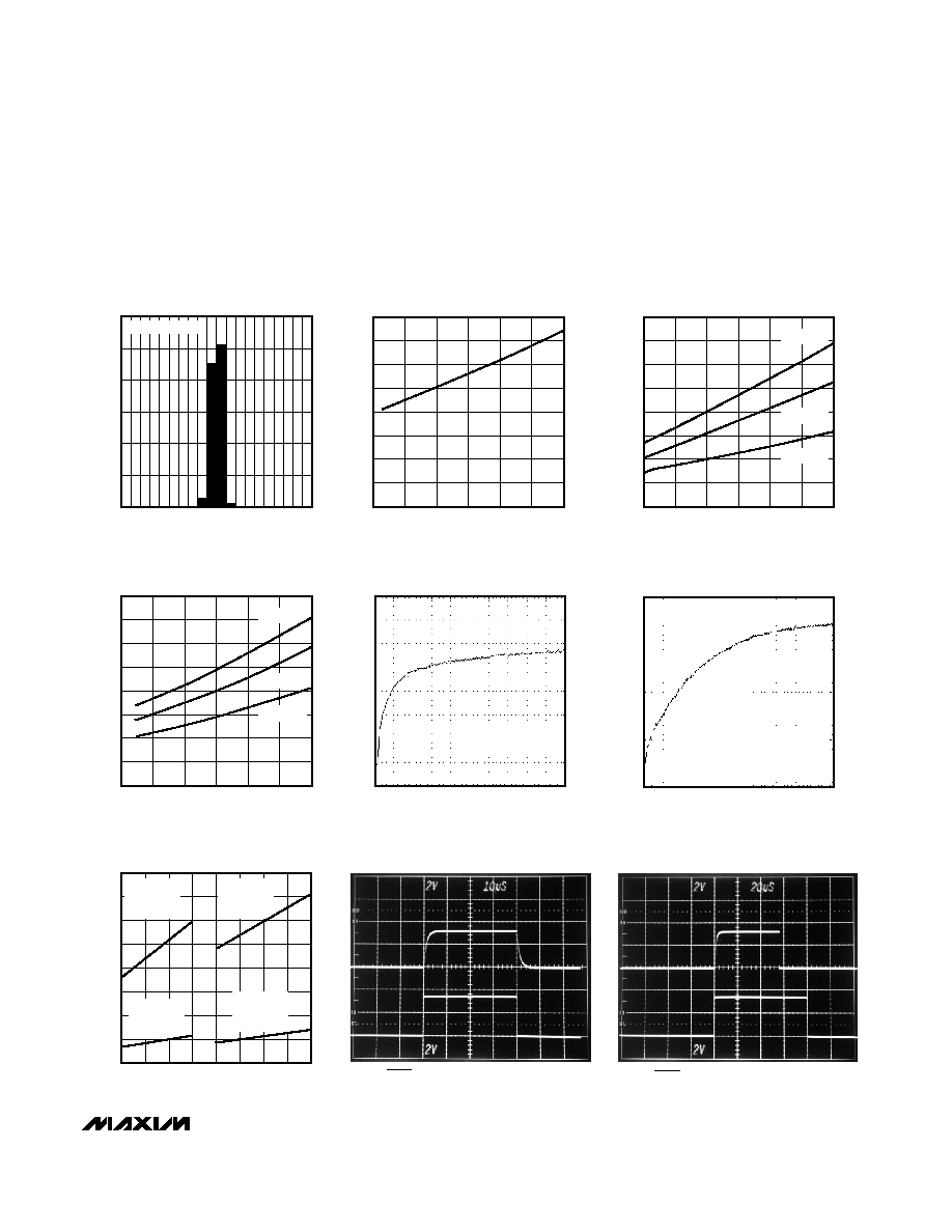
SUPPLY CURRENT
vs. TEMPERATURE
MAX6501 TOC01
TEMPERATURE (∞C)
SUPPLY CURRENT (
µ
A)
0
100
200
300
400
500
600
700
800
-55
5
-25
35
65
95
125
MAX6502/MAX6504
OUTPUT SOURCE RESISTANCE
vs. TEMPERATURE
MAX6501 TOC02
TEMPERATURE (∞C)
OUTPUT SOURCE RESISTANCE (
)
V
CC
= 2.7V
V
CC
= 5.0V
V
CC
= 3.3V
0
20
40
60
80
100
120
140
160
-55
5
-25
35
65
95
125
OUTPUT SINK RESISTANCE
vs. TEMPERATURE
MAX6501 TOC03
TEMPERATURE (∞C)
OUTPUT SINK RESISTANCE (
)
V
CC
= 2.7V
V
CC
= 5.0V
V
CC
= 3.3V
+15∞C/div
+100∞C
+25∞C
SOT23 THERMAL STEP RESPONSE
IN PERFLUORINATED FLUID
MAX6501 TOC4
5sec/div
MOUNTED ON 0.75in
2
OF 2 oz. COPPER
0
4
2
8
6
10
12
14
16
-5
15
-25
-45
35
55
75
95
115
HYSTERESIS
vs. TRIP TEMPERATURE
MAX6501 TOC8
TRIP TEMPERATURE (∞C)
HYSTERESIS (
∞
C)
MAX6503
MAX6504
HYST = V
CC
MAX6501
MAX6502
HYST = V
CC
MAX6501
MAX6502
HYST = GND
MAX6503
MAX6504
HYST = GND
+12.5∞C/div
+100∞C
+25∞C
SOT23 THERMAL STEP RESPONSE
IN STILL AIR
MAX6501 TOC5
20sec/div
MOUNTED ON 0.75in
2
OF 2 oz. COPPER
TRACE A: TOVER VOLTAGE, R
PULL-UP
= 100k
TRACE B: V
CC
PULSE DRIVEN FROM 3.3V CMOS LOGIC OUTPUT
MAX6501 START-UP AND POWER-DOWN
(T
< T
TH
)
B
A
MAX6501 TOC07
TRACE A: TOVER VOLTAGE, R
PULL-UP
= 100k
TRACE B: V
CC
PULSE DRIVEN FROM 3.3V CMOS LOGIC OUTPUT
MAX6501 START-UP DELAY
(T
> T
TH
)
B
A
MAX6501 TOC07A
__________________________________________Typical Operating Characteristics
(V
CC
= +5V, R
PULL-UP
= 100k
(MAX6501/MAX6503), T
A
= +25∞C, unless otherwise noted.)
0
10
20
30
40
50
60
-5
-4
-3
-2
-1
0
1
2
3
4
5
TRIP THRESHOLD ACCURACY
MAX6501 TOC-A
ACCURACY (∞C)
PERCENTAGE OF PARTS SAMPLED (%)
SAMPLE SIZE = 300

MAX6501≠MAX6504
Low-Cost, +2.7V to +5.5V, Micropower
Temperature Switches in SOT23 and TO-220
4
_______________________________________________________________________________________
Pin Description
1, 2
1, 2
Ground. Not internally connected. Tie both ground pins togeth-
er close to the chip. Pin 2 provides the lowest thermal resis-
tance to the die.
1, 2
PIN
1, 2
GND
3
3
Hysteresis Input. Connect HYST to GND for +2∞C hysteresis, or
connect to V
CC
for +10∞C hysteresis.
3
3
HYST
4
4
Supply Input (+2.7V to +5.5V)
5
--
Open-Drain, Active-Low Output. TOVER goes low when the die
temperature exceeds the factory-programmed temperature
threshold. Connect to a 100k
pull-up resistor. May be pulled
up to a voltage higher than V
CC
.
--
--
TOVER
4
4
V
CC
--
5
Push-Pull Active-High Output. TOVER goes high when the die tem-
perature exceeds the factory-programmed temperature threshold.
--
--
Open-Drain, Active-Low Output. TUNDER goes low when the
die temperature goes below the factory-programmed tempera-
ture threshold. Connect to a 100k
pull-up resistor. May be
pulled up to a voltage higher than V
CC
.
5
--
TUNDER
--
--
Push-Pull Active-High Output. TUNDER goes high when the die tem-
perature falls below the factory-programmed temperature threshold.
--
5
TUNDER
--
--
TOVER
MAX6502
MAX6501
MAX6503
MAX6504
NAME
FUNCTION
________________General Description
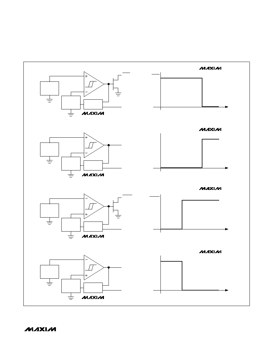
The MAX6501≠MAX6504 fully integrated temperature
switches incorporate two temperature-dependent refer-
ences and a comparator. One reference exhibits a pos-
itive temperature coefficient and the other a negative
temperature coefficient (Figure 1). The temperature at
which the two reference voltages are equal determines
the temperature trip point. Pin-selectable +2∞C or
+10∞C hysteresis keeps the output from oscillating
when the die temperature approaches the threshold
temperature. The MAX6501/MAX6503 have an active-
low, open-drain output structure that can only sink cur-
rent. The MAX6502/MAX6504 have an active-high,
push-pull output structure that can sink or source cur-
rent. The internal power-on reset circuit guarantees the
output is at T
TH
= +25∞C state at start-up for 50µs.
The MAX6501≠MAX6504 are available with factory-
preset temperature thresholds from -45∞C to +115∞C in
10∞C increments. Table 1 lists the available temperature
threshold ranges. The MAX6501/MAX6503 outputs are
intended to interface with a microprocessor (µP) reset
input (Figure 2). The MAX6502/MAX6504 outputs are
intended for applications such as driving a fan control
(Figure 3).
Hysteresis Input
The HYST pin is a CMOS-compatible input that selects
hysteresis at either a high level (+10∞C for HYST = V
CC
)
or a low level (+2∞C for HYST = GND). Hysteresis pre-
vents the output from oscillating when the temperature
approaches the trip point. The HYST pin should not
float. Drive HYST close to ground or V
CC
. Other input
voltages cause increased supply current. The actual
amount of hysteresis depends on the part's pro-
grammed trip threshold. (See the Typical Operating
Characteristics graphs.)
Table 1. Factory-Programmed Threshold
Range
+35∞C < T
TH
< +115∞C
+35∞C < T
TH
< +115∞C
THRESHOLD (T
TH
) RANGE
-45∞C < T
TH
< +15∞C
-45∞C < T
TH
< +15∞C
MAX6503
MAX6504
MAX6501
MAX6502
PART
MAX6501≠MAX6504
Low-Cost, +2.7V to +5.5V, Micropower
Temperature Switches in SOT23 and TO-220
_______________________________________________________________________________________
5
POSITIVE
TEMPCO
REFERENCE
NEGATIVE
TEMPCO
REFERENCE
HYST
NETWORK
TOVER
HYST
TOVER
TEMP
COLD
+25∞C
T
TH
V
MAX6501
POSITIVE
TEMPCO
REFERENCE
NEGATIVE
TEMPCO
REFERENCE
HYST
NETWORK
TOVER
HYST
TOVER
TEMP
COLD
+25∞C
T
TH
HOT
HOT
V
POSITIVE
TEMPCO
REFERENCE
NEGATIVE
TEMPCO
REFERENCE
HYST
NETWORK
TUNDER
HYST
TUNDER
TEMP
COLD
T
TH
+25∞C
HOT
V
POSITIVE
TEMPCO
REFERENCE
NEGATIVE
TEMPCO
REFERENCE
HYST
NETWORK
TUNDER
HYST
TUNDER
TEMP
COLD
T
TH
+25∞C
HOT
V
MAX6502
MAX6503
MAX6504
MAX6501
WITH 100k
PULL-UP
MAX6504
MAX6503
WITH 100k
PULL-UP
MAX6502
Figure 1. Block and Functional Diagrams