 | ÐлекÑÑоннÑй компоненÑ: MAX6681 | СкаÑаÑÑ:  PDF PDF  ZIP ZIP |
Äîêóìåíòàöèÿ è îïèñàíèÿ www.docs.chipfind.ru
General Description
The MAX6680/MAX6681 are precise, two-channel digi-
tal thermometers. Each accurately measures the tem-
perature of its own die and one remote PN junction and
reports the temperature on a 2-wire serial interface. The
remote junction can be a diode-connected transistor
like the low-cost NPN type 2N3904 or PNP type
2N3906. The remote junction can also be a common-
collector PNP, such as a substrate PNP of a micro-
processor.
The MAX6680/MAX6681 include pin-programmable
default temperature thresholds for the OVERT output,
which provides fail-safe clock throttling or system shut-
down. In addition, the devices are pin programmable to
select whether the OVERT output responds to either the
local, remote, or both temperatures.
The 2-wire serial interface accepts standard System
Management Bus (SMBus)TM commands such as Write
Byte, Read Byte, Send Byte, and Receive Byte to read
the temperature data and program the alarm thresholds
and conversion rate. The MAX6680/MAX6681 can func-
tion autonomously with a programmable conversion
rate, which allows the control of supply current and
temperature update rate to match system needs. For
conversion rates of 4Hz or less, the remote sensor tem-
perature can be represented in extended mode as 10
bits + sign with a resolution of 0.125°C. When the con-
version rate is 8Hz, output data is 7 bits + sign with a
resolution of 1°C. The MAX6680/MAX6681 also include
an SMBus timeout feature to enhance system reliability.
The MAX6681 is an upgrade to the MAX6654. The
MAX6680/MAX6681 remote accuracy is ±1°C with no
calibration needed. They are available in a 16-pin
QSOP package and operate throughout the -55°C to
+125°C temperature range.
Applications
Features
o Two Alarm Outputs: ALERT and OVERT
o Pin-Programmable Threshold for OVERT Limit
o Programmable Under/Overtemperature ALERT
Limit
o Dual Channel: Measures Remote and Local
Temperature
o 11-Bit, 0.125°C Resolution for Remote Temperature
Measurements
o High Accuracy ±1°C (max) from +60°C to +100°C
(Remote)
o No Calibration Required
o SMBus/I
2
CTM-Compatible Interface
o SMBus Timeout Prevents SMBus Lockup
MAX6680/MAX6681
±1°C Fail-Safe Remote/Local Temperature
Sensors with SMBus Interface
________________________________________________________________ Maxim Integrated Products
1
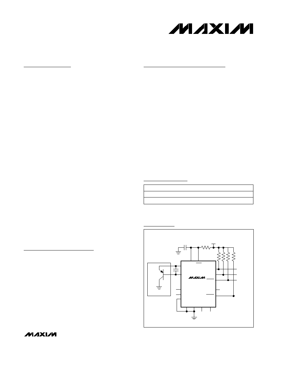
CLOCK
DATA
TO SYSTEM
SHUTDOWN
STBY
CRIT1
CRIT0
GND
OVERT
SMBCLK
RESET
SMBDATA
V
CC
INTERRUPT
TO
µP
0.1
µF
2200pF
DXN
MICROPROCESSOR
DXP
200
10k
EACH
ALERT
3.3V
INT_SEL
SENS_SEL
ADD1
ADD0
MAX6680
MAX6681
Typical Operating Circuit
Ordering Information
19-2305; Rev 0; 4/02
For pricing, delivery, and ordering information, please contact Maxim/Dallas Direct! at
1-888-629-4642, or visit Maxim's website at www.maxim-ic.com.
PART
TEMP RANGE
PIN-PACKAGE
MAX6680MEE
-55
°C to +125°C
16 QSOP
MAX6681MEE
-55
°C to +125°C
16 QSOP
SMBus is a trademark of Intel Corp.
I
2
C is a trademark of Philips Corp.
Pin Configurations appear at end of data sheet.
Desktop Computers
Notebook
Computers
Servers
Thin Clients
Workstations
MAX6680/MAX6681
±1°C Fail-Safe Remote/Local Temperature
Sensors with SMBus Interface
2
_______________________________________________________________________________________
ABSOLUTE MAXIMUM RATINGS
ELECTRICAL CHARACTERISTICS
(Circuit of Typical Operating Circuit, V
CC
= 3.0V to 5.5V, T
A
= -25°C to +125°C, unless otherwise specified. Typical values are at V
CC
= 3.3V and T
A
= +25°C.)
Stresses beyond those listed under "Absolute Maximum Ratings" may cause permanent damage to the device. These are stress ratings only, and functional
operation of the device at these or any other conditions beyond those indicated in the operational sections of the specifications is not implied. Exposure to
absolute maximum rating conditions for extended periods may affect device reliability.
V
CC
...........................................................................-0.3V to +6V
DXP.............................................................-0.3V to (V
CC
+ 0.3V)
DXN ......................................................................-0.3V to +0.8V
SMBCLK, SMBDATA, ALERT, OVERT .....................-0.3V to +6V
RESET, INT_SEL, STBY, ADD0, ADD1.....................-0.3V to +6V
CRIT1, CRIT0, SENS_SEL ........................................-0.3V to +6V
SMBDATA, ALERT, OVERT, Current ..................-1mA to +50mA
DXN Current ......................................................................±1mA
Continuous Power Dissipation (T
A
= +70°C)
16-Pin QSOP (derate 8.3mW/°C above +70°C) ..........664mW
Junction Temperature .....................................................+150°C
Storage Temperature Range ............................-65°C to +150°C
Lead Temperature (soldering, 10s) ................................+300°C
PARAMETER
SYMBOL
CONDITIONS
MIN
TYP
MAX
UNITS
1
°C
Temperature Resolution,
Legacy Mode
8
Bits
0.125
°C
Temperature Resolution,
Extended Mode
11
Bits
T
RJ
= +60°C to +100°C, V
CC
= 3.3V
-1.0
+1.0
T
RJ
= +50°C to +120°C, V
CC
= 3.3V
-2.0
+2.0
Rem ote Tem p er atur e E r r or ( N ote 1)
T
RJ
= -55°C to +125°C, V
CC
= 3.3V
-3.0
+3.0
°C
T
A
= +60°C to +100°C, V
CC
= 3.3V
-1.5
+1.5
T
A
= 0°C to +125°C, V
CC
= 3.3V
-3.0
+3.0
Local Temperature Error
T
A
= -55°C to +125°C, V
CC
= 3.3V (Note 2)
-5.0
+5.0
°C
Line Regulation
3.0V
V
CC
5.5V
0.2
0.6
m
°C/V
Supply Voltage Range
V
CC
3.0
5.5
V
Undervoltage Lockout Threshold
UVLO
Falling edge of V
CC
disables ADC
2.60
2.80
2.95
V
Undervoltage Lockout Hysteresis
90
mV
Power-On Reset (POR)
Threshold
V
CC
, falling edge
1.5
2.0
2.5
V
POR Threshold Hysteresis
90
mV
Legacy
62.5
Conversion Time
Extended
125
ms
Standby Supply Current
SMBus static
3
10
µA
Operating Current
During conversion
0.55
1.0
mA
0.25 conversions/s
35
70
Average Operating Current
(Note 3)
2 conversions/s
120
180
µA
DXP and DXN Leakage Current
In standby mode
2
µA
High level
80
100
120
Remote-Diode Source Current
I
RJ
Low level
8
10
12
µA
MAX6680/MAX6681
±1°C Fail-Safe Remote/Local Temperature
Sensors with SMBus Interface
_______________________________________________________________________________________
3
ELECTRICAL CHARACTERISTICS (continued)
(Circuit of Typical Operating Circuit, V
CC
= 3.0V to 5.5V, T
A
= -25°C to +125°C, unless otherwise specified. Typical values are at V
CC
= 3.3V and T
A
= +25°C.)
Note 1: T
A
= +25°C to +85°C.
Note 2: If both the local and the remote junction are below T
A
= -20°C, then V
CC
> 3.15V.
Note 3: Conversions done in extended mode. For legacy mode, current is approximately half.
Note 4: Timing specifications guaranteed by design.
Note 5: The serial interface resets when SMBCLK or SMBDATA is low for more than t
TIMEOUT
.
Note 6: A transition must internally provide at least a hold time to bridge the undefined region (300ns max) of SMBCLK's falling edge.
PARAMETER
SYMBOL
CONDITIONS
MIN
TYP
MAX
UNITS
CRIT0, CRIT1, ADD0, ADD1, RESET, INT_SEL, SENS_SEL
Logic Input Low Voltage
V
IL
0.8
V
Logic Input High Voltage
V
IH
2.4
V
Input Leakage Current
I
LEAK
-1
+1
µA
(ALERT, OVERT)
Output Low Sink Current
V
OL
= 0.4V
1
mA
Output High Leakage Current
V
OH
= 5.5V
1
µA
SMBus INTERFACE (SMBCLK, SMBDATA, STBY)
Logic Input Low Voltage
V
IL
0.8
V
V
CC
= 3.0V
2.2
Logic Input High Voltage
V
IH
V
CC
= 5.5V
2.4
V
Input Leakage Current
I
LEAK
V
IN
= GND or V
CC
±2
µA
Output Low Sink Current
I
OL
V
OL
= 0.6V
6
mA
Input Capacitance
C
IN
5
pF
SMBus-COMPATIBLE TIMING (Note 5)
Serial Clock Frequency (Note 5)
f
SCL
100
kHz
Bus Free Time Between STOP
and START Condition
t
BUF
4.7
µs
START Condition Setup Time
4.7
µs
Repeat START Condition Setup
Time
t
SU:STA
90% to 90%
50
ns
START Condition Hold Time
t
HD:STA
10% of SMBDATA to 90% of SMBCLK
4
µs
STOP Condition Setup Time
t
SU:STO
90% of SMDCLK to 90% of SMBDATA
4
µs
Clock Low Period
t
LOW
10% to 10%
4.7
µs
Clock High Period
t
HIGH
90% to 90%
4
µs
Data Setup Time (Note 6)
t
HD:DAT
250
ns
Receive SCL/SDA Rise Time
t
R
1
µs
Receive SCL/SDA Fall Time
t
F
300
ns
Pulse Width of Spike Suppressed
t
SP
0
50
ns
SMBus Timeout (Note 5)
SMBDATA low period for interface reset
25
37
45
ms
MAX6680/MAX6681
±1°C Fail-Safe Remote/Local Temperature
Sensors with SMBus Interface
4
_______________________________________________________________________________________
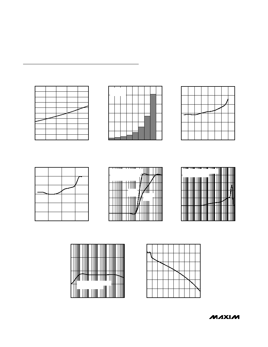
Typical Operating Characteristics
(T
A
= +25°C, unless otherwise noted.)
MAX6680/81 toc01
SUPPLY VOLTAGE (V)
STANDBY SUPPLY CURRENT (
µ
A)
5.0
4.5
4.0
3.5
1
2
3
4
5
6
7
8
9
10
0
3.0
5.5
STANDBY SUPPLY CURRENT
vs. SUPPLY VOLTAGE
MAX6680/81 toc02
CONVERSION RATE (Hz)
OPERATING SUPPLY CURRENT (
µ
A)
8.0000
4.0000
2.0000
1.0000
0.5000
0.2500
0.1250
100
200
300
400
500
600
0
0.0625
AVERAGE OPERATING SUPPLY CURRENT
vs. CONVERSION RATE
8Hz IS 1
°C
RESOLUTION
MAX6680/81 toc03
TEMPERATURE (
°C)
TEMPERATURE ERROR (
°
C)
125
100
75
50
25
0
-25
-2
-1
0
1
2
3
-3
-50
150
TEMPERATURE ERROR
vs. REMOTE-DIODE TEMPERATURE
MAX6680/81 toc04
TEMPERATURE (
°C)
TEMPERATURE ERROR (
°
C)
100
50
0
-2
-1
0
1
2
3
-3
-50
150
LOCAL TEMPERATURE ERROR
vs. DIE TEMPERATURE
MAX6680/81 toc05
FREQUENCY (Hz)
TEMPERATURE ERROR (
°
C)
1M
10k
100
0
0.2
0.4
0.6
0.8
1.0
1.2
-0.2
1
10M
100k
1k
10
100M
TEMPERATURE ERROR
vs. POWER-SUPPLY NOISE FREQUENCY
V
IN
= 100mV SQUARE WAVE
APPLIED TO V
CC
WITH NO
0.1
µF V
CC
CAPACITOR
LOCAL
DIODE
REMOTE
DIODE
MAX6680/81 toc06
FREQUENCY (Hz)
TEMPERATURE ERROR (
°
C)
10M
1M
100k
10k
1k
100
10
-1
0
1
2
3
4
5
-2
1
100M
TEMPERATURE ERROR
vs. COMMON-MODE NOISE FREQUENCY
V
IN
= 100mV
P-P
SQUARE WAVE
AC-COUPLED TO DXN
MAX6680/81 toc07
FREQUENCY (Hz)
TEMPERATURE ERROR (
°
C)
10M
1M
100k
10k
1k
0
1
2
3
-1
100
100M
TEMPERATURE ERROR
vs. DIFFERENTIAL NOISE FREQUENCY
V
IN
= 10mV
P-P
SQUARE WAVE
APPLIED TO DXP-DXN
MAX6680/81 toc08
DXP-DXN CAPACITANCE (nF)
TEMPERATURE ERROR (
°
C)
90
80
70
60
50
40
30
20
10
-4
-3
-2
-1
0
1
-5
0
100
TEMPERATURE ERROR
vs. DXP-DXN CAPACITANCE
MAX6680/MAX6681
±1°C Fail-Safe Remote/Local Temperature
Sensors with SMBus Interface
_______________________________________________________________________________________
5
Pin Description
PIN
MAX6680
MAX6681
NAME
FUNCTION
1
2
V
CC
Supply Voltage Input, 3V to 5.5V. Bypass V
CC
to GND with a 0.1µF capacitor.
A 200
series resistor is recommended, but not required for additional noise
filtering. See the Typical Operating Circuit.
2, 5
1, 5
CRIT1,
CRIT0
Hardware-Programmable Default Alarm Threshold for
OVERT Limits. Use Table
4 to set default temperatures.
3
3
DXP
Combined Remote-Diode Current Source and A/D Positive Input for Remote-
Diode Channel. DO NOT LEAVE DXP FLOATING; connect DXP to DXN if no
remote diode is used. Place a 2200pF capacitor between DXP and DXN for
noise filtering.
4
4
DXN
Combined Remote-Diode Current Sink and A/D Negative Input. DXN is
internally biased to one diode drop above ground.
6
6
ADD1
SMBus Address Select Pin (Table 9). ADD0 and ADD1 are sampled upon
power-up. Excess capacitance (>50pF) at the address pins when floating may
cause address-recognition problems.
7
7
RESET
Reset Input. Drive RESET high to set all registers to their default values (POR
state). Drive RESET low or leave floating for normal operation.
8
8
GND
Ground
9
9
OVERT
Overtemperature Active-Low Output. Open drain.
10
10
ADD0
SMBus Slave Address Select Pin (see ADD1).
11
11
ALERT
SMBus Alert (Interrupt) Active-Low Output. Open drain.
12
12
SMBDATA
SMBus Serial-Data Input/Output, Open Drain
13
13
INT_SEL
Input. Connect high or leave floating to conform to the standard SMBus
ALERT
protocol. See the
ALERT Interrupts section. Connect to GND to invoke
comparator mode, where
ALERT is asserted whenever any of the temperature
conditions is violated by the remote sensor. In this mode,
ALERT can only be
deasserted by the condition returning within the temperature limits by enabling
the mask bit in the Configuration register.
14
14
SMBCLK
SMBus Serial-Clock Input
15
15
STBY
Input. Hardware Standby. Connect to ground to place in device in standby.
Supply current drops below 10µA and all registers' data are maintained.
Input. Selects which temperature sensor (local, remote, or both) activates
OVERT.
16
16
SENS_SEL
High = Local, Low = Remote, Open = Local and Remote