 | –≠–ª–µ–∫—Ç—Ä–æ–Ω–Ω—ã–π –∫–æ–º–ø–æ–Ω–µ–Ω—Ç: MAX6786 | –°–∫–∞—á–∞—Ç—å:  PDF PDF  ZIP ZIP |

MAX6782≠MAX6790
Low-Power, 1% Accurate, Dual-/Triple-/Quad-Level
Battery Monitors in Small TDFN and TQFN Packages
________________________________________________________________
Maxim Integrated Products
1
19-0541; Rev 0; 8/06
For pricing, delivery, and ordering information, please contact Maxim/Dallas Direct! at
1-888-629-4642, or visit Maxim's website at www.maxim-ic.com.
o
o
o
o
o
o
o
o
o
o
o
General Description
Features
1% Accurate Threshold Specified Over Full
Temperature Range
Dual-/Triple-/Quad, Low-Battery Output Options
Low 5.7µA Battery Current
Open-Drain or Push-Pull Outputs
Fixed or Adjustable Hysteresis
Low Input Bias Current
Guaranteed Valid Low-Battery-Output Logic State
Down to V
BATT
= 1.05V
Reverse-Battery Protection
Immune to Short Battery Transients
Fully Specified from -40∞C to +85∞C
Small TDFN and TQFN Packages
The MAX6782≠MAX6790 are low-power, 1% accurate,
dual-/triple-/quad-level battery monitors offered in small
TDFN and TQFN packages. These devices are ideal for
monitoring single lithium-ion (Li+) cells, or multicell alka-
line/NiCd/NiMH power sources. These devices feature
fixed and adjustable hysteresis options to eliminate out-
put chattering associated with battery-voltage monitors.
The MAX6782/MAX6783 offer four battery monitors in a
single package with factory-set (0.5%, 5%, 10%) or
adjustable hysteresis. The MAX6784/MAX6785 provide
three battery monitors with factory-set (0.5%, 5%, 10%)
or adjustable hysteresis. The MAX6786/MAX6787/
MAX6788 offer two battery monitors with external inputs
for setting the rising and falling thresholds, allowing
external hysteresis control. The MAX6789/MAX6790 fea-
ture quad-level overvoltage detectors with complemen-
tary outputs.
The MAX6782≠MAX6790 are offered with either open-drain
or push-pull outputs. The MAX6782/MAX6784/MAX6786/
MAX6789 are available with push-pull outputs while the
MAX6783/MAX6785/MAX6787/MAX6790 are available with
open-drain outputs. The MAX6788 is available with one
open-drain output and one push-pull output (see the
Selector Guide). This family of devices is offered in space-
saving TDFN and TQFN packages and is fully specified
over the -40∞C to +85∞C extended temperature range.
Ordering Information
Selector Guide
Applications
Ordering Information continued at end of data sheet.
+
Denotes lead-free package.
*
Future product--contact factory for availability.
**
EP = Exposed paddle.
The MAX6782/MAX6783/MAX6784/MAX6785 are available with
factory-trimmed hysteresis. Specify trim by replacing "_" with
"A" for 0.5%, "B" for 5%, or "C" for 10% hysteresis.
Pin Configuration and Typical Operating Circuit appear at
end of data sheet.
PART
TEMP RANGE
PIN-
PACKAGE
PKG
CODE
MAX6782TE_+
-40∞C to +85∞C
16 TQFN-EP**
T1633-4
MAX6783TE_+
-40∞C to +85∞C
16 TQFN-EP**
T1633-4
MAX6784TC_+*
-40∞C to +85∞C
12 TQFN-EP**
T1233-1
MAX6785TC_+
-40∞C to +85∞C
12 TQFN-EP**
T1233-1
PART
MONITOR LEVEL
LBO OUTPUT
OV
OV
OUTPUT TYPE
HYSTERESIS
MAX6782TE_+
4
Quad
--
--
Push-Pull
Fixed/Adj
MAX6783TE_+
4
Quad
--
--
Open Drain
Fixed/Adj
MAX6784TC_+
3
Triple
--
--
Push-Pull
Fixed/Adj
MAX6785TC_+
3
Triple
--
--
Open Drain
Fixed/Adj
MAX6786TA+
2
Dual
--
--
Push-Pull
Adj
MAX6787TA+
2
Dual
--
--
Open Drain
Adj
MAX6788TA+
2
Dual
--
--
Push-Pull/Open Drain
Adj
MAX6789TB+
4
--
Single
Single
Push-Pull
--
MAX6790TB+
4
--
Single
Single
Open Drain
--
Note: All devices are available in tape and reel in 2.5k increments. For tape and reel order, add a "T" after the "+" to complete the part
number.
Battery-Powered Systems
(Single-Cell Li+ or
Multicell NiMH, NiCd,
Alkaline)
Cell Phones/Cordless
Phones
Pagers
Portable Medical Devices
PDAs
Electronic Toys
MP3 Players

MAX6782≠MAX6790
Low-Power, 1% Accurate, Dual-/Triple-/Quad-Level
Battery Monitors in Small TDFN and TQFN Packages
2
_______________________________________________________________________________________
ABSOLUTE MAXIMUM RATINGS
ELECTRICAL CHARACTERISTICS
(V
BATT
= 1.6V to 5.5V, T
A
= -40∞C to +85∞C, unless otherwise specified. Typical values are at T
A
= +25∞C.) (Note 1)
Stresses beyond those listed under "Absolute Maximum Ratings" may cause permanent damage to the device. These are stress ratings only, and functional
operation of the device at these or any other conditions beyond those indicated in the operational sections of the specifications is not implied. Exposure to
absolute maximum rating conditions for extended periods may affect device reliability.
(All voltages referenced to GND.)
BATT.........................................................................-0.3V to +6V
IN1≠IN4, LBH1, LBL1,
LBH2, LBL2 ..................-0.3V to Min ((V
BATT
+ 0.3V) and +6V)
HADJ1≠HADJ4, REF .......-0.3V to Min ((V
BATT
+ 0.3V) and +6V)
LBO1≠LBO4 (push-pull)..-0.3V to Min ((V
BATT
+ 0.3V) and +6V)
LBO1≠LBO4 (open drain).........................................-0.3V to +6V
Input Current (all pins) ........................................................20mA
Output Current (all pins) .....................................................20mA
Continuous Power Dissipation (T
A
= +70∞C)
8-Pin TDFN (derate 23.8mW/∞C above +70∞C) ..........1905mW
10-Pin TDFN (derate 24.4mW/∞C above +70∞C) ........1951mW
12-Pin Thin QFN (derate 16.7mW/∞C above +70∞C) ..1333mW
16-Pin Thin QFN (derate 20.8mW/∞C above +70∞C) ..1667mW
Operating Temperature Range ...........................-40∞C to +85∞C
Junction Temperature .............................................+150∞C
Storage Temperature Range .............................-65∞C to +150∞C
Lead Temperature (soldering, 10s) .................................+300∞C
PARAMETER
SYMBOL
CONDITIONS
MIN
TYP
MAX
UNITS
T
A
= 0∞C to +70∞C
1.05
5.5
Operating Voltage Range
(Note 2)
V
BATT
T
A
= -40∞C to +85∞C
1.2
5.5
V
V
BATT
= 3.7V, no load
6.3
10
µA
Supply Current
I
Q
V
BATT
= 1.8V, no load
5.7
µA
Startup Time (Note 3)
V
BATT
rising from 0 to 1.6V
5
ms
MAX6782/MAX6783/MAX6784/MAX6785
0.5% hysteresis (A version)
0.5994
0.6055
0.6115
5% hysteresis (B version)
0.5723
0.5781
0.5839
IN_ Falling Threshold (Note 4)
V
INF
10% hysteresis (C version)
0.5422
0.5477
0.5531
V
IN_ Rising Threshold (Note 4)
V
INR
0.6024
0.6085
0.6146
V
IN_, HADJ_ Input Leakage
Current
V
IN_,
V
HADJ_
0.3V
5
nA
Reference Output
V
REF
0.6024
0.6085
0.6146
V
Reference Load Regulation
I
REF
= 0 to 1mA
0.3
mV/mA
Reference Temperature
Coefficient
TEMPCO
15
ppm/∞C
Reference Short-Circuit Current
20
mA
Hysteresis Adjustment Range
0.4
V
REF
V
Hysteresis Adjustment Logic Low
V
HALL
0.07
V
Hysteresis Adjustment Logic
High
V
HALH
0.17
V
MAX6786/MAX6787/MAX6788
LBL_, LBH_ Threshold
V
TH
0.6024
0.6085
0.6146
V
LBL_, LBH_ Input Leakage
Current
V
LBL
, V
LBH_
0.3V
5
nA
MAX6782≠MAX6790
Low-Power, 1% Accurate, Dual-/Triple-/Quad-Level
Battery Monitors in Small TDFN and TQFN Packages
_______________________________________________________________________________________
3
ELECTRICAL CHARACTERISTICS (continued)
(V
BATT
= 1.6V to 5.5V, T
A
= -40∞C to +85∞C, unless otherwise specified. Typical values are at T
A
= +25∞C.) (Note 1)
PARAMETER
SYMBOL
CONDITIONS
MIN
TYP
MAX
UNITS
MAX6782≠MAX6788
LBO_ Propagation Delay
t
PD
±100mV overdrive
30
µs
V
BATT
1.2V, I
SINK
= 100µA
0.3
V
V
BATT
2.7V, I
SINK
= 1.2mA
0.3
V
LBO_ Output Low Voltage (Push-
Pull or Open Drain)
V
OL
V
BATT
4.5V, I
SINK
= 3.2mA
0.4
V
V
BATT
1.6V, I
SOURCE
= 10µA
0.8 x
V
BATT
V
V
BATT
2.7V, I
SOURCE
= 500µA
0.8 x
V
BATT
V
LBO_ Output High Voltage
(Push-Pull) (Note 5)
V
OH
V
BATT
4.5V, I
SOURCE
= 800µA
0.8 x
V
BATT
V
LBO_ Output Leakage Current
(Open Drain)
Output not asserted, V
LBO_
= 0 or 5V
500
nA
MAX6789/MAX6790
IN_ Rising Threshold
V
TH+
0.6024
0.6085
0.6146
V
IN_ Hysteresis
31
mV
IN_ Input Leakage Current
V
IN_
0.3V
5
nA
OV, OV Delay Time
t
PD
±100mV overdrive
30
µs
V
BATT
1.6V, I
SINK
= 100µA, output
asserted
0.3
V
BATT
2.7V, I
SINK
= 1.2mA, output
asserted
0.3
OV Output Low Voltage (Push-
Pull or Open Drain)
V
OL
V
BATT
4.5V, I
SINK
= 3.2mA, output
asserted
0.4
V
V
BATT
1.2V, I
SOURCE
= 10µA, output not
asserted
0.8 x
V
BATT
V
BATT
2.7V, I
SOURCE
= 500µA, output not
asserted
0.8 x
V
BATT
OV Output High Voltage (Push-
Pull) (Note 5)
V
OH
V
BATT
4.5V, I
SINK
= 800µA, output not
asserted
0.8 x
V
BATT
V
OV Output Leakage Current
(Open Drain)
Output not asserted, V
OV
, V
OV
= 0 or 5V
500
nA
V
BATT
1.2V, I
SINK
= 100µA, output not
asserted
0.3
V
BATT
2.7V, I
SINK
= 1.2mA, output not
asserted
0.3
OV Output Low Voltage
(Push-Pull or Open Drain)
V
OL
V
BATT
4.5V, I
SINK
= 3.2mA, output not
asserted
0.4
V

MAX6782≠MAX6790
Low-Power, 1% Accurate, Dual-/Triple-/Quad-Level
Battery Monitors in Small TDFN and TQFN Packages
4
_______________________________________________________________________________________
ELECTRICAL CHARACTERISTICS (continued)
(V
BATT
= 1.6V to 5.5V, T
A
= -40∞C to +85∞C, unless otherwise specified. Typical values are at T
A
= +25∞C.) (Note 1)
PARAMETER
SYMBOL
CONDITIONS
MIN
TYP
MAX
UNITS
V
BATT
1.6V, I
SOURCE
= 10µA, output
asserted
0.8 x
V
BATT
V
BATT
2.7V, I
SOURCE
= 500µA, output
asserted
0.8 x
V
BATT
OV Output High Voltage (Push-
Pull ) (Note 5)
V
OH
V
BATT
4.5V, I
SOURCE
= 800µA, output
asserted
0.8 x
V
BATT
V
OV Output Leakage Current
(Open Drain)
Output asserted, V
OV
= 0 or 5V
500
nA
CLEAR Input Low Voltage
V
IL
0.3 x
V
BATT
V
CLEAR Input High Voltage
V
IH
0.7 x
V
BATT
V
CLEAR Pullup Resistance
25
80
k
CLEAR Minimum Pulse Width
1
µs
CLEAR Delay Time
t
CLD
300
ns
Note 1: Devices are tested at T
A
= +25∞C and guaranteed by design for T
A
= T
MIN
to T
MAX
as specified.
Note 2: Operating voltage range ensures low battery output is in the correct state. Minimum battery voltage for electrical specifica-
tion is 1.6V.
Note 3: Reference and threshold accuracy is only guaranteed after the startup time. Startup time is guaranteed by design.
Note 4: The rising threshold is guaranteed to be higher than the falling threshold.
Note 5: The source current is the total source current from all outputs.
MAX6782≠MAX6790
Low-Power, 1% Accurate, Dual-/Triple-/Quad-Level
Battery Monitors in Small TDFN and TQFN Packages
_______________________________________________________________________________________
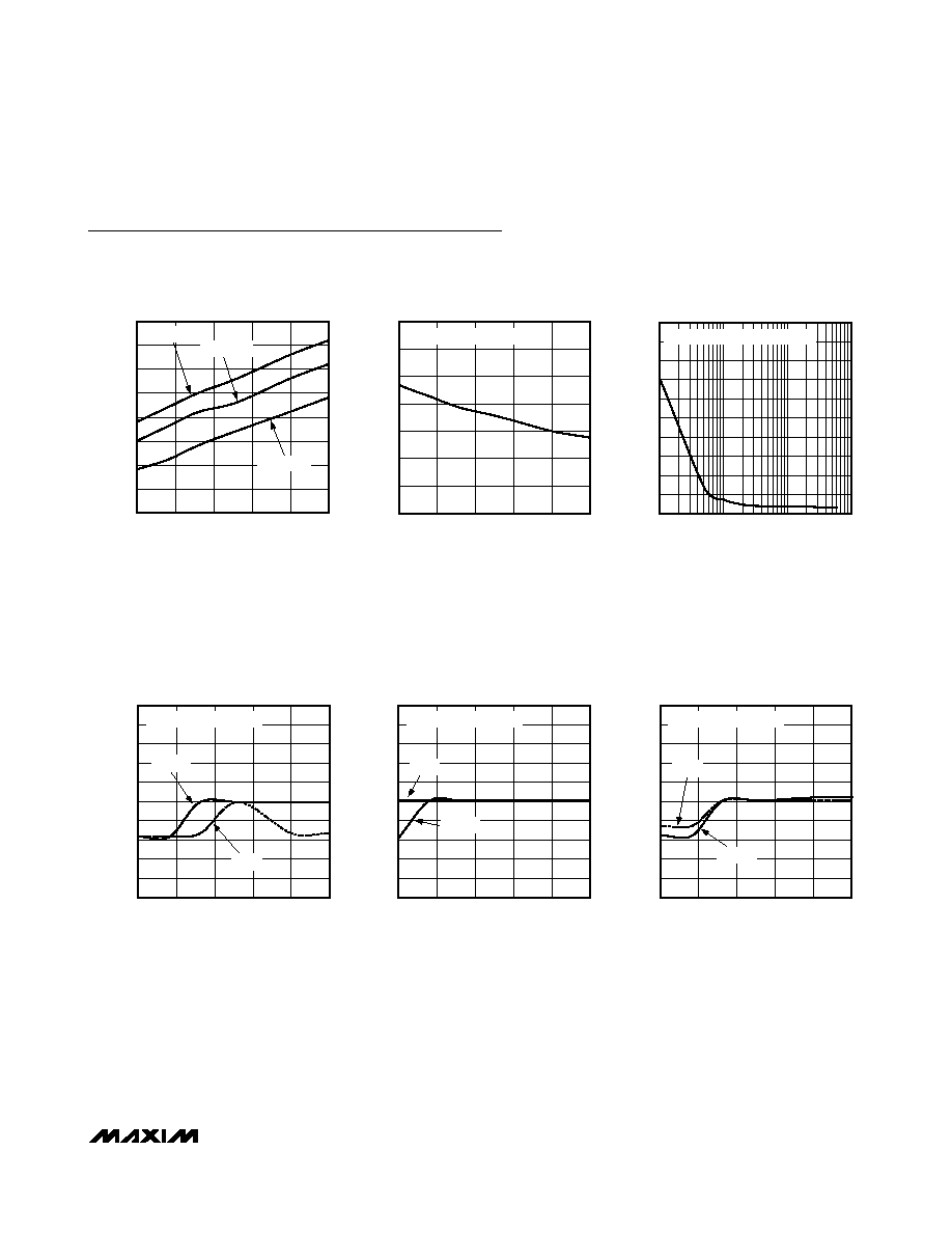
5
SUPPLY CURRENT
vs. TEMPERATURE
MAX6782 toc01
TEMPERATURE (∞C)
SUPPLY CURRENT (
µ
A)
60
35
-15
10
4.5
5.0
5.5
6.0
6.5
7.0
7.5
8.0
4.0
-40
85
V
BATT
= 5V
V
BATT
= 3.6V
V
BATT
= 1.8V
PROPAGATION DELAY
vs. TEMPERATURE
MAX6782 toc02
TEMPERATURE (∞C)
PROPAGATION DELAY (
µ
s)
60
35
10
-15
10
20
30
40
50
60
70
0
-40
85
V
IN_
= ±100mV OVERDRIVE
MAXIMUM TRANSIENT DURATION
vs. THRESHOLD OVERDRIVE
MAX6782 toc03
THRESHOLD OVERDRIVE (mV)
MAXIMUM TRANSIENT DURATION (
µ
s)
100
10
100
200
300
400
500
600
700
800
900
1000
0
1
1000
OUTPUT ASSERTED ABOVE THIS LINE
NORMALIZED THRESHOLD VOLTAGES
vs. TEMPERATURE (MAX6782TEA)
MAX6782 toc04
TEMPERATURE (∞C)
NORMALIZED THRESHOLD (V)
60
35
10
-15
0.996
0.997
0.998
0.999
1.000
1.001
1.002
1.003
1.004
1.005
0.995
-40
85
NORMALIZED AT T
A
= +25∞C
FALLING
RISING
NORMALIZED THRESHOLD VOLTAGES
vs. TEMPERATURE (MAX6782TEB)
MAX6782 toc05
TEMPERATURE (∞C)
NORMALIZED THRESHOLD (V)
60
35
10
-15
0.996
0.997
0.998
0.999
1.000
1.001
1.002
1.003
1.004
1.005
0.995
-40
85
NORMALIZED AT T
A
= +25∞C
FALLING
RISING
NORMALIZED THRESHOLD VOLTAGES
vs. TEMPERATURE (MAX6782TEC)
MAX6782 toc06
TEMPERATURE (∞C)
NORMALIZED THRESHOLD (V)
60
35
10
-15
0.996
0.997
0.998
0.999
1.000
1.001
1.002
1.003
1.004
1.005
0.995
-40
85
NORMALIZED AT T
A
= +25∞C
FALLING
RISING
Typical Operating Characteristics
(V
BATT
= 3.6V, T
A
= +25∞C, unless otherwise noted.)