 | –≠–ª–µ–∫—Ç—Ä–æ–Ω–Ω—ã–π –∫–æ–º–ø–æ–Ω–µ–Ω—Ç: MAX688 | –°–∫–∞—á–∞—Ç—å:  PDF PDF  ZIP ZIP |
_______________General Description
The MAX687/MAX688/MAX689 low-dropout linear regula-
tors operate with an input-to-output voltage differential lim-
ited only by an external PNP transistor. Outputs are fixed
at 3.3V (MAX687/MAX688) or 3.0V (MAX689). The only
external components required are a PNP pass transistor
and output, compensation, and bypass capacitors. Base
drive to the external transistor is at least 10mA, permitting
output currents to exceed 1A when using high-gain tran-
sistors (
> 100). Output current limiting is implemented
by limiting the external transistor's base current. Output
voltage monitoring and shutdown functions are included.
The 3.3V MAX687 automatically shuts down whenever
the output voltage drops below 2.96V. An internal
power-fail comparator also monitors the output and pro-
vides an early warning of low output voltage before the
device shuts down. When shut down, the output is
latched off until the ON input is pulsed. Turning off the
power supply in this way prevents battery damage due
to excessive discharge or cell-reversal. Typical applica-
tions include portable telephones and other battery-pow-
ered equipment where the power supply must be
disabled when the battery voltage is low.
The MAX688 and MAX689 do not have an automatic
shutdown function, and are identical except for their
output voltages. Each device has an active-low shut-
down-control input, used to turn its output on or off at
any time. As SHDN falls, the device enters a standby
mode before fully shutting down. When in standby, the
reference and comparators are fully operational, per-
mitting the transition from normal mode to standby
mode to occur at a precise voltage level on SHDN.
________________________Applications
High-Efficiency Linear Regulator
Battery-Powered Devices
Portable Instruments
Portable Telephones
Power Supply or Backup Supply for Memory
____________________________Features
o
Fixed Outputs:
3.3V (MAX687/MAX688)
3.0V (MAX689)
o
Directly Drives External PNP Transistor
o
10mA Min Base-Current Drive for >1A Output
o
Low Dropout Voltage:
100mV Dropout at 650mA Output (FZT749)
40mV Dropout at 200mA Output (FZT749)
0.8V Dropout at 4A Output
o
Power-Fail Output Monitors the Output Voltage
o
Automatic, Latched Shutdown when Output Falls Out
of Regulation (MAX687)
o
Precision Threshold Shutdown Control
(MAX688/MAX689)
o
Low Supply Current:
150µA Operating
<1µA Shutdown
o
2.7V to 11.0V Supply Range
o
8-Pin DIP/SO/µMAX Packages
o
<2mV Line Transient with 3.4V to 3.6V Input
o
Output Accuracy <±2%
______________Ordering Information
Ordering Information continued at end of data sheet.
MAX687/MAX688/MAX689
High-Accuracy, Low-Dropout
Linear Regulators
________________________________________________________________
Maxim Integrated Products
1
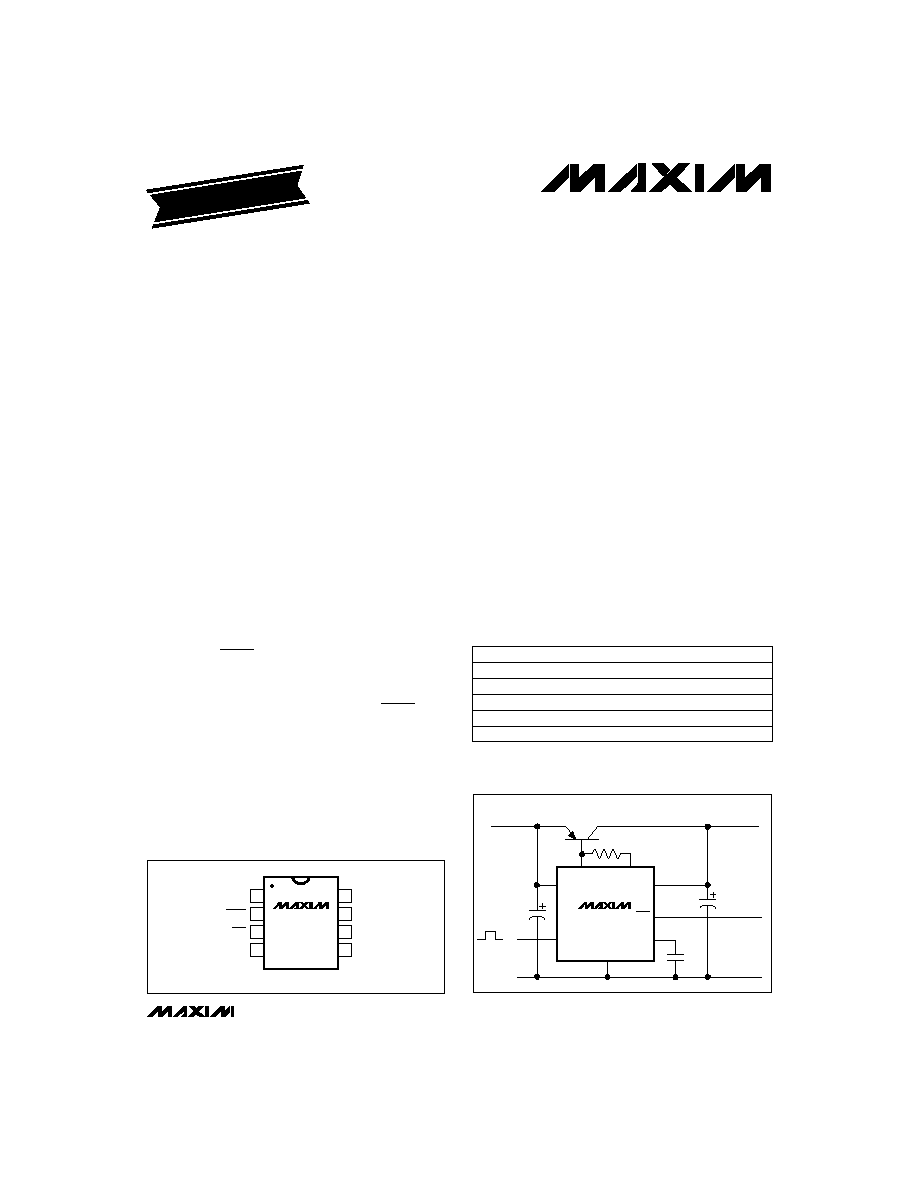
MAX687
Q1
FZT749
R
B
12
BASE
GND
C1
2.2
µ
F
IN
BLIM
OUT
POWER-FAIL
OUTPUT
3.3V @ 500mA
PFO
CC
+3.5V to +5V INPUT
ON
C3
10nF
ON
GND
C2
68
µ
F
__________Typical Operating Circuit
1
2
3
4
8
7
6
5
CC
BASE
BLIM
OUT
GND
PFO
(ON) SHDN
IN
MAX687
MAX688
MAX689
DIP/SO/
µ
MAX
TOP VIEW
( ) ARE FOR MAX687
__________________Pin Configuration
Call toll free 1-800-998-8800 for free samples or literature.
19-0329; Rev 0; 12/94
PART
MAX687
CPA
MAX687CSA
MAX687CUA
0∞C to +70∞C
0∞C to +70∞C
0∞C to +70∞C
TEMP. RANGE
PIN-PACKAGE
8 Plastic DIP
8 SO
8 µMAX
EVALUATION KIT MANUAL
FOLLOWS DATA SHEET
MAX687EPA
MAX687ESA
-40∞C to +85∞C
-40∞C to +85∞C
8 Plastic DIP
8 SO
MAX687/MAX688/MAX689
High-Accuracy, Low-Dropout
Linear Regulators
2
_______________________________________________________________________________________
ABSOLUTE MAXIMUM RATINGS
ELECTRICAL CHARACTERISTICS
(V
IN
= 3.8V, SHDN = V
IN
(MAX688/MAX689), R
B
= 0
, C1 = 2.2µF, C2 = 10µF, C3 = 10nF, T
A
= T
MIN
to T
MAX
, unless otherwise
noted. Typical values are at T
A
= +25∞C.)
Stresses beyond those listed under "Absolute Maximum Ratings" may cause permanent damage to the device. These are stress ratings only, and functional
operation of the device at these or any other conditions beyond those indicated in the operational sections of the specifications is not implied. Exposure to
absolute maximum rating conditions for extended periods may affect device reliability.
Input Supply Voltage IN to GND ............................................12V
Terminal Voltages to GND
PFO (MAX687) ........................................-0.3V to V
OUT
+ 0.3V
PFO (MAX688/MAX689) ......................................-0.3V to 12V
All Remaining Pins .....................................-0.3V to V
IN
+ 0.3V
PFO Sink Current ...............................................................10mA
PFO Source Current (MAX687)...........................................10mA
Continuous Power Dissipation (T
A
= +70∞C)
Plastic DIP (derate 9.09mW/∞C above +70∞C) ............727mW
SO (derate 5.88mW/∞C above +70∞C) .........................471mW
µMAX (derate 4.1mW/∞C above +70∞C) ......................330mW
Operating Temperature Ranges
MAX68_C_A .......................................................0∞C to +70∞C
MAX68_E_A ....................................................-40∞C to +85∞C
Storage Temperature Range .............................-65∞C to +165∞C
Lead Temperature (soldering, 10sec) .............................+300∞C
MAX687/MAX688
(Note 1)
V
BASE
= V
IN
- 1V
PNP = FZT749, I
LOAD
= 100mA (Note 4)
V
IN
= 3.8V,
PNP = FZT749,
no load
(Note 3)
1µA
I
BASE
10mA
R
B
is connected from BASE to BLIM (
),
R
B
= 0
to 100
CONDITIONS
µF
10
C2
Load Capacitance
%
2
Start-Up Overshoot
µs
300
Start-Up Time
mA
70
100
130
R
B
+ 5
R
B
+ 5
R
B
+ 5
Base-Current Limit
V
3.2
3.3
3.4
V
OUT
Output Voltage
V
2.7
11.0
V
IN
Supply Voltage
mA
10
20
40
I
BASE
BASE Sink Current
< 0.02
1
11
25
µA
150
250
I
GND
Supply Current
3.13
3.3
3.47
mV
40
V
IN
- V
OUT
Dropout Voltage (Note 2)
mV/V
0.4
1.4
Line Regulation
mV
45
60
Load Regulation
UNITS
MIN
TYP
MAX
SYMBOL
PARAMETER
V
IN
= 3.8V, I
BASE
= 1mA
3.8V
V
IN
11.0V,
1µA
I
BASE
10mA
PNP = FZT749, I
LOAD
= 200mA, C2 = 20µF
3.8V
V
IN
11.0V,
I
BASE
= 1mA
MAX687/MAX688
MAX689
2.9
3.0
3.1
2.85
3.0
3.15
V
IN
= 3.5V, I
BASE
= 1mA
3.5V
V
IN
11.0V,
1µA
I
BASE
10mA
MAX689
3.5V
V
IN
11.0V,
I
BASE
= 1mA
0.4
1.4
On
Standby,
MAX688/MAX689
Shutdown
LINEAR REGULATOR

MAX687/MAX688/MAX689
High-Accuracy, Low-Dropout
Linear Regulators
_______________________________________________________________________________________
3
Note 1:
Minimum V
IN
for regulated V
OUT
depends on the characteristics of the external PNP transistor, and on the load. The refer-
ence and comparators are functional down to the minimum voltage specified, but the output may not be in regulation.
Note 2:
Dropout voltage is defined as V
IN
- V
OUT
when V
OUT
is 50mV below its value at V
IN
= V
NOM
+ 1V.
Note 3:
The start-up time specification is the time taken from ON or SHDN rising to BASE sinking current. V
OUT
rise time is longer
and is a function of load capacitance, C2, and load resistance, R
L
.
Note 4:
Minimum load capacitance is a function of R
L
. Minimum C2 = 10µF for loads up to 100mA and 1µF/10mA for higher loads.
ESR of C2 should be no larger than 1/100 of R
L
. Guaranteed by design.
Note 5:
The nominal output voltage, V
NOM
, is defined under the default conditions of testing: V
IN
= 3.8V, I
BASE
= 1mA, T
A
= T
MIN
to T
MAX
.
ELECTRICAL CHARACTERISTICS (continued)
(V
IN
= 3.8V, SHDN = V
IN
(MAX688/MAX689), R
B
= 0
, C1 = 2.2µF, C2 = 10µF, C3 = 10nF, T
A
= T
MIN
to T
MAX
, unless otherwise
noted. Typical values are at T
A
= +25∞C.)
Falling V
OUT
, comparators monitor V
OUT
Glitch immunity
Rising SHDN, standby
on
Shutdown
Standby
Falling V
OUT
, comparators monitor V
OUT
On, SHDN falling
Output turns on
CONDITIONS
µs
100
PFO, SHDN Transient Rejection
mV
70
SHDN Hysteresis
0.2
V
SSD
1.0
1.2
V
SSY
V
1.25
V
SON
SHDN Threshold Voltages
mV
110
170
V
NOM
-
V
PFT
PFO Threshold Voltage Below
V
NOM
(Note 5)
mV
7
PFO Hysteresis
V
2.96
V
SD
Shutdown Threshold Voltage
V
1.0
V
IH
ON Threshold Voltage
UNITS
MIN
TYP
MAX
SYMBOL
PARAMETER
I
SOURCE
= 50µA, part on, V
IN
= 2.7V
V
V
OUT
- 0.3
V
OH
PFO Output Voltage High
I
SINK
= 1.2mA, V
IN
= 2.7V
V
0.06
0.3
V
OL
PFO Output Voltage Low
Output remains off
0.2
V
IL
nA
0.2
100
ON Input Leakage Current
Falling V
OUT
, com-
parators monitor V
OUT
V
3.07
3.13
3.19
V
PFT
PFO Threshold Voltage
MAX688
MAX689
2.77
2.85
2.89
V
SHDN
= 1.23V
nA
-25
25
SHDN Input Current
10Hz
f
10kHz, I
LOAD
= 200mA
V
PFO
= 11V, V
SHDN
> 1.25V
I
SINK
= 1.2mA, V
IN
= 2.7V
µA
1
66
e
n
Output Noise Voltage
PFO Off Leakage Current
V
0.06
0.3
V
OL
PFO Output Voltage Low
10Hz
f
1MHz, I
LOAD
= 200mA
µV
RMS
105
Falling V
OUT
, comparators monitor V
OUT
mV
20
70
V
PFT
- V
SD
Shutdown Threshold Voltage
Below V
PFT
mV
7
PFO Hysteresis
MAX688/MAX689: SHDN, PFO
MAX687: ON, PFO, SHDN
MAX687/MAX688/MAX689
High-Accuracy, Low-Dropout
Linear Regulators
4
_______________________________________________________________________________________
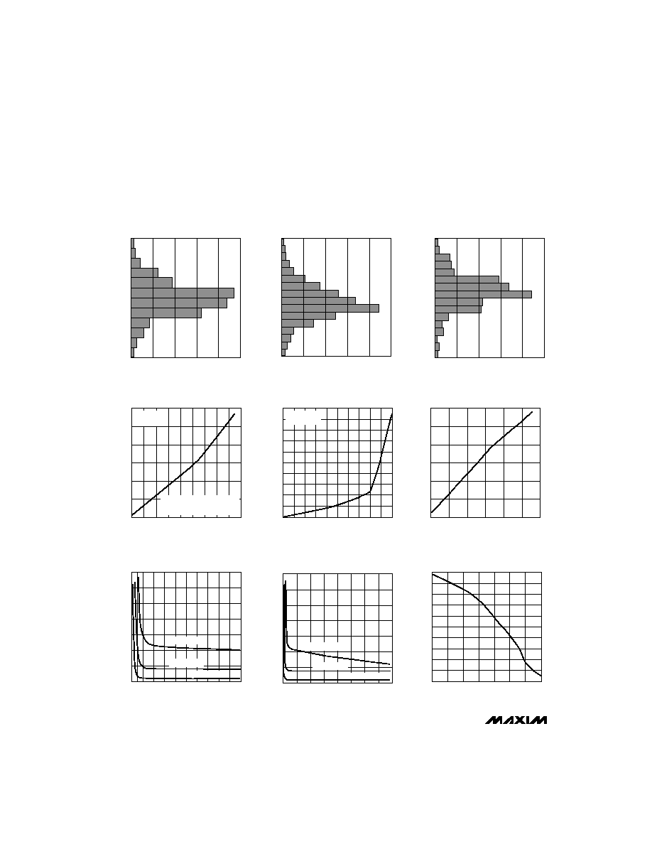
__________________________________________Typical Operating Characteristics
(Circuits of Figures 1 and 2, V
IN
= 5V, Q1 = FZT749, T
A
= +25∞C, unless otherwise noted.)
3.29679
3.29904
3.29455
3.29231
3.29007
3.28783
3.30128
3.30352
3.30576
3.30800
3.31024
3.31248
3.31472
3.31696
3.31920
3.32145
0
50
100
NUMBER OF UNITS
250
200
150
MAX688
OUTPUT VOLTAGE DISTRIBUTION
MAX687/9-01
OUTPUT VOLTAGE (V)
3.28365
3.28722
3.29078
3.29435
3.29792
3.30149
3.30505
3.30862
3.31219
3.31576
3.31932
3.32289
0
50
100
250
200
150
MAX687
OUTPUT VOLTAGE DISTRIBUTION
MAX687/9-02
OUTPUT VOLTAGE (V)
NUMBER OF UNITS
2.98975
2.99150
2.99324
2.99499
2.99674
2.99848
3.00023
3.00198
3.00372
3.00547
3.00721
3.00896
3.01071
3.01245
3.01420
3.01595
0
50
100
250
200
150
MAX689
OUTPUT VOLTAGE DISTRIBUTION
MAX687/9-03
OUTPUT VOLTAGE (V)
NUMBER OF UNITS
7
6
5
4
3
2
1
0
0
0.1 0.2 0.3 0.4 0.5 0.6 0.7 0.8 0.9 1.0
GND CURRENT vs. DROPOUT VOLTAGE
MAX687/9-7
V
IN
- V
OUT
(V)
GND CURRENT (mA)
300mA LOAD
100mA LOAD
10mA LOAD
0
0.05
0.10
0.15
0.20
0.25
0.30
0
200
600
1000
1400
1800
DROPOUT VOLTAGE
vs. LOAD CURRENT
MAX687/9-05
LOAD CURRENT (mA)
V
IN
- V
OUT
(V)
Q1 = FZT749
R
B
= 0
OBSERVE MAXIMUM POWER
DISSIPATION LIMIT OF
EXTERNAL PASS TRANSISTOR.
0
1
2
3
4
5
6
0
200
400
600
800
1000 1200
GND CURRENT
vs. LOAD CURRENT
MAX687/9-06
LOAD CURRENT (mA)
GND CURRENT (mA)
7
6
5
4
3
2
1
0
0
8
1
2
3
4
5
7
6
GND CURRENT vs. DROPOUT VOLTAGE
MAX687/9-8
V
IN
- V
OUT
(V)
GND CURRENT (mA)
300mA LOAD
100mA LOAD
10mA LOAD
146
126
NO-LOAD SUPPLY CURRENT
vs. TEMPERATURE
130
128
134
132
138
136
142
144
140
MAX687/9-9
TEMPERATURE (∞C)
SUPPLY CURRENT (
µ
A)
-55
-25
0
25
50
75
100
125
1.0
0
0
200
600
1000
DROPOUT VOLTAGE
vs. LOAD CURRENT
0.2
0.1
0.4
0.3
0.6
0.5
0.8
0.9
0.7
MAX687/9-5
LOAD CURRENT (mA)
V
IN
- V
OUT
(V)
400
800
Q1 = 2N2907
R
B
= 0
MAX687/MAX688/MAX689
High-Accuracy, Low-Dropout
Linear Regulators
_______________________________________________________________________________________
5
0
0.0500
0.1000
0.1500
0.2000
0.2500
0.3000
-55
-25
0
25
50
75
100
125
SHUTDOWN SUPPLY CURRENT
vs. TEMPERATURE
MAX687/9-10
TEMPERATURE (∞C)
SHUTDOWN SUPPLY CURRENT (
µ
A)
3.280
3.285
3.290
3.295
3.300
3.305
3.310
3.315
OUTPUT VOLTAGE
vs. TEMPERATURE
MAX687/9-11
TEMPERATURE (∞C)
OUTPUT VOLTAGE (V)
-55
-25
0
25
50
75
100
125
I
LOAD
= 70mA
C1 = 2.2
µ
F
C2 = 20
µ
F
C3 = 10nF
LINE-TRANSIENT RESPONSE
V
OUT
3.3V
1mV/div
V
IN
3.6V
V
IN
3.4V
2ms/div
I
LOAD
= 200mA
C1 = 2.2
µ
F
C2 = 20
µ
F
C3 = 10nF
LINE-TRANSIENT RESPONSE
V
OUT
3.3V
1mV/div
V
IN
3.6V
V
IN
3.4V
2ms/div
V
IN
= 3.4V
LOAD-TRANSIENT RESPONSE
V
OUT
3.3V
10mV/div
500mA
0mA
100
µ
s/div
I
LOAD
200mA/div
V
IN
= 3.5V
LOAD-TRANSIENT RESPONSE
V
OUT
3.3V
10mV/div
500mA
0mA
100
µ
s/div
I
LOAD
200mA/div
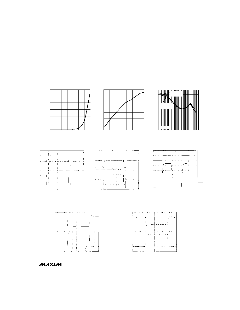
____________________________Typical Operating Characteristics (continued)
(Circuits of Figures 1 and 2, V
IN
= 5V, Q1 = FZT749, T
A
= +25∞C, unless otherwise noted.)
I
LOAD
= 500mA
C1 = 2.2
µ
F
C2 = 68
µ
F
C3 = 10nF
MAX687/MAX688
POWER-UP AND EXIT FROM SHUTDOWN
V
IN
5V/div
V
OUT
1V/div
SHDN
5V/div
1ms/div
80
0
10
100
1k
10k
100k
MAX687/MAX688
RIPPLE REJECTION vs. FREQUENCY
10
20
MAX687/9-16
FREQUENCY (Hz)
RIPPLE REJECTION (dB)
30
40
50
60
70
C2 = 20
µ
F
V
IN
= 4.3V Min
I
LOAD
= 20mA
V
IN
= 3.6V Min
I
LOAD
= 200mA