General Description
The MAX6901 3-wire serial interface real-time clock in a
TDFN package contains a real-time clock/calendar and
31 x 8 bits of static RAM (SRAM). The real-time
clock/calendar provides seconds, minutes, hours, day,
date, month, year, and century information. A
time/date-programmable polled ALARM is included in
the MAX6901. The end of the month date is automati-
cally adjusted for months with fewer than 31 days,
including corrections for leap year up to the year 2100.
The clock operates in either the 24hr or 12hr format
with an AM/PM indicator. A push-pull 32kHz output is
also included. The MAX6901 operates with a supply
voltage of +2V to +5.5V, is available in the ultra-small 8-
pin TDFN package, and works over the industrial tem-
perature range, -40∞C to +85∞C.
Applications
Point-of-Sale Equipment
Intelligent Instruments
Fax Machines
Battery-Powered Products
Portable Instruments
Features
o Real-Time Clock Counts Seconds, Minutes,
Hours, Day of Week, Date of Month, Month, Year,
and Century
o Leap-Year Compensation Valid up to Year 2100
o Wide +2V to +5.5V Operating Voltage Range
o 3-Wire Serial Interface, 2MHz at 5V, 500kHz at 2V
o 31 x 8-Bit SRAM for Scratchpad Data Storage
o Uses Standard 32.768kHz, 12.5pF Watch Crystal
o Low Timekeeping Current (400nA at 2V)
o Single-Byte or Multiple-Byte (Burst Mode)
Data Transfer for Read or Write of Clock
Registers or SRAM
o 8-Pin 3mm x 3mm x 0.8mm TDFN
Surface-Mount Package
o Push-Pull 32.768kHz Clock Output
o Programmable Time/Date Polled ALARM Function
o No External Crystal Bias Resistors or Capacitors
Required
MAX6901
3-Wire Serial RTC in a TDFN
________________________________________________________________ Maxim Integrated Products
1
19-2085; Rev 1; 2/03
Ordering Information
PART
TEMP
RANGE
PIN-
PACKAGE
TOP
MARK
MAX6901ETA-T
-40
∞C to +85∞C
8 TDFN
AGV
Related Real-Time Clock Products
PART
SERIAL
INTERFACE
ALARM
(bits)
ALARM
FUNCTION
OUTPUT
FREQUENCY
PIN-PACKAGE
MAX6900
I
2
CTM compatible
31 x 8
--
--
6 TDFN
MAX6901
3 wire
31 x 8
Polled
32kHz
8 TDFN
MAX6902
SPI
TM
compatible
31 x 8
Polled
--
8 TDFN
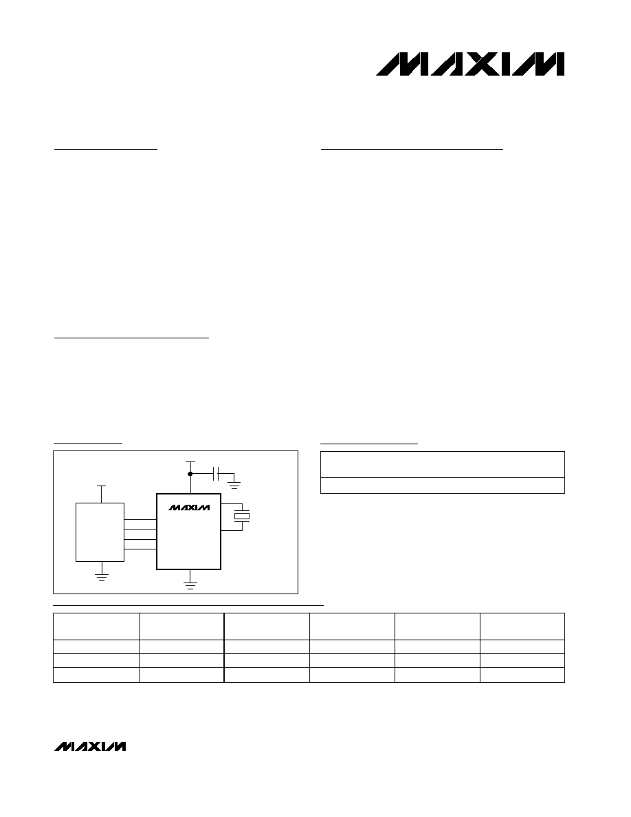
Pin Configuration appears at end of data sheet.
Functional Diagram appears at end of data sheet.
µC
0.1
µF
32.768kHz
CRYSTAL
1
4
3
6
2
5
3.3V
3.3V
MAX6901
7
8
P1.0
CLKIN
P1.1
P1.2
SCLK
CS
I/O
32KHZ
GND
V
CC
X1
X2
Typical Operating Circuit
For pricing, delivery, and ordering information, please contact Maxim/Dallas Direct! at
1-888-629-4642, or visit Maxim's website at www.maxim-ic.com.
I
2
C is a trademark of Philips Corp. Purchase of I
2
C components of Maxim Integrated Products, Inc., or one of its sublicensed Associated
Companies, conveys a license under the Philips I
2
C Patent rights to use these components in an I
2
C system provided that the system
conforms to the I
2
C Standard Specification as defined by Philips.
SPI is a trademark of Motorola, Inc.

MAX6901
3-Wire Serial RTC in a TDFN
2
_______________________________________________________________________________________
ABSOLUTE MAXIMUM RATINGS
Stresses beyond those listed under "Absolute Maximum Ratings" may cause permanent damage to the device. These are stress ratings only, and functional
operation of the device at these or any other conditions beyond those indicated in the operational sections of the specifications is not implied. Exposure to
absolute maximum rating conditions for extended periods may affect device reliability.
V
CC
to GND.............................................................-0.3V to +6V
All Other Pins to GND ................................-0.3V to (Vcc + 0.3V)
Current into Any Pin..........................................................±20mA
Rate-of-Rise, V
CC
............................................................100V/µs
Continuous Power Dissipation (T
A
= +70∞C)
8-Pin TDFN (derate 24.4mW/∞C above +70∞C) .........1951.0mW
Junction Temperature .....................................................+150∞C
Storage Temperature Range .............................-65∞C to +150∞C
ESD Protection (all pins, Human Body Model) ..................2000V
Lead Temperature (soldering, 10s) .................................+300∞C
DC ELECTRICAL CHARACTERISTICS
(V
CC
= +2.0V to +5.5V, T
A
= -40∞C to +85∞C, unless otherwise noted. Typical values are at V
CC
= +3.3V, T
A
= +25∞C.) (Note 1)
PARAMETER
SYMBOL
CONDITIONS
MIN
TYP
MAX
UNITS
Operating Voltage Range
V
CC
2
5.5
V
V
CC
= +2.0V
0
∞C < T
A
< +70
∞C
110
Active Supply Current (Note 2)
I
CC
V
CC
= +5V
0
∞C < T
A
< +70
∞C
800
µA
V
CC
= +2.0V
0.4
0.7
Timekeeping Supply Current
(Note 3)
I
TK
V
CC
= +5V
1.3
1.7
µA
32kHz OUTPUT
V
CC
= +2.0V, I
SOURCE
= -0.4mA
1.8
Output High Voltage (Note 5)
V
OH
V
CC
= +5.0V, I
SOURCE
= -1mA
4.5
V
V
CC
= +2.0V, I
SINK
= 1.5mA
0.4
Output Low Voltage (Note 5)
V
OL
V
CC
= +5.0V, I
SINK
= 4mA
0.4
V
Duty Cycle
40
%
Output Leakage Current
V
IN
= 0 to V
CC
, 32kHz output disabled
-10
10
nA
3-WIRE DIGITAL INPUTS AND OUTPUTS (SCLK, I/O, CS)
V
CC
= +2.0V
1.4
Input High Voltage
V
IH
V
CC
= +5.0V
2.2
V
V
CC
= +2.0V
0.6
Input Low Voltage
V
IL
V
CC
= +5.0V
0.8
V
Input Leakage Current
V
IN
= 0 to V
CC
-10
10
nA
SCLK, RST Capacitance
5
pF
I/O Capacitance
10
pF
V
CC
= +2.0V, I
SINK
= 1.5mA
0.4
I/O Output Low Voltage
V
OL
V
CC
= +5.0V, I
SINK
= 4mA
0.4
V
V
CC
= +2.0V, I
SOURCE
= -0.4mA
1.8
I/O Output High Voltage
V
OH
V
CC
= +5.0V, I
SOURCE
= -1mA
4.5
V
MAX6901
3-Wire Serial RTC in a TDFN
_______________________________________________________________________________________
3
Note 1: All parameters are 100% tested at T
A
= +25∞C. Limits over temperature are guaranteed by design and not production tested.
Note 2: I
CC
is specified with the I/O grounded, CS high, SCLK = 2MHz at V
CC
= +5V; SCLK = 500kHz at V
CC
= +2.0V, 32kHz output
enabled, and no load on 32kHz output.
Note 3: Timekeeping current is specified with CS = GND, SCLK = GND, I/O = GND, 32kHz = GND, and 32kHz disabled.
Note 4: All values referred to V
IH
min and V
IL
max levels.
Note 5: Guaranteed by design. Not production tested.
AC ELECTRICAL CHARACTERISTICS
(V
CC
= +2.0V to +5.5V, T
A
= -40∞C to +85∞C, unless otherwise noted. Typical values are at V
CC
= +3.3V, T
A
= +25∞C.) (Figures 4, 5
and Notes 1, 4)
PARAMETER
SYMBOL
CONDITIONS
MIN
TYP
MAX
UNITS
OSCILLATOR
X1 to Ground Capacitance (Note 5)
25
pF
X2 to Ground Capacitance (Note 5)
25
pF
3-WIRE SERIAL TIMING
V
CC
= +2V
200
Data to CLK Setup
t
DC
V
CC
= +5V
50
ns
V
CC
= +2V
280
CLK to Data Hold
t
CDH
V
CC
= +5V
70
ns
V
CC
= +2V
800
CLK to Data Delay
t
CDD
C
L
= 50pF
V
CC
= +5V
200
ns
V
CC
= +2V
1000
CLK Low Time
t
CL
V
CC
= +5V
250
ns
V
CC
= +2V
1000
CLK High Time
t
CH
V
CC
= +5V
250
ns
V
CC
= +2V
DC
0.5
CLK Frequency
f
CLK
V
CC
= +5V
DC
2.0
MHz
V
CC
= +2V
2000
CLK Rise and Fall Time
t
R
, t
F
V
CC
= +5V
500
ns
V
CC
= +2V
4
CS to CLK Setup
t
CC
V
CC
= +5V
1
µs
V
CC
= +2V
240
CLK to CS Hold
t
CCH
V
CC
= +5V
60
ns
V
CC
= +2V
4
CS Inactive Time
t
CWH
V
CC
= +5V
1
µs
V
CC
= +2V
0
280
CS to I/O High Z
t
CDZ
R
L
= 1k
, C
L
= 60pF
V
CC
= +5V
0
70
ns
V
CC
= +2V
0
280
SCLK to I/O High Z
t
CCZ
R
L
= 1k
, C
L
= 60pF
V
CC
= +5V
0
70
ns
MAX6901
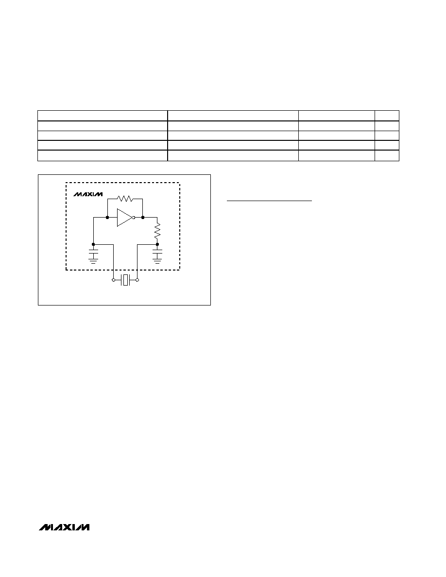
Detailed Description
The MAX6901 is a real-time clock/calendar with a 3-wire
serial interface and 31
8 bits of SRAM. It provides sec-
onds, minutes, hours, day of the week, date of the
month, month, and year information, held in seven 8-bit
timekeeping registers (Functional Diagram). An on-chip
32.768kHz oscillator circuit does not require any exter-
nal resistors or capacitors to operate. Table 1 specifies
the parameters for the external crystal, and Figure 1
shows a functional schematic of the oscillator circuit.
The MAX6901's register addresses and definitions are
described in Tables 2 and 3. Time and calendar data
are stored in the registers in binary coded decimal
(BCD) format. A polled alarm function is included for
scheduled timing of user-defined times or intervals.
Command and Control
Address/Command Byte
Each data transfer into or out of the MAX6901 is initiat-
ed by an Address/Command byte. The Address/
Command byte specifies which registers are to be
accessed, and if the access is a read or a write. Table
2 shows the Address/Command bytes and their associ-
ated registers, and Table 3 lists the hex codes for all
read and write operations. The Address/Command
bytes are input LSB (bit 0) first. Bit 0 specifies a write
(logic 0) or read (logic 1). Bits 1 to 5 specify the desig-
nated register to be written or read. Bit 6 specifies reg-
ister data (logic 0), or RAM data (logic 1). The MSB (bit
7) must be logic 1. If the MSB is a zero, writes to the
MAX6901 are disabled.
3-Wire Serial RTC in a TDFN
4
_______________________________________________________________________________________
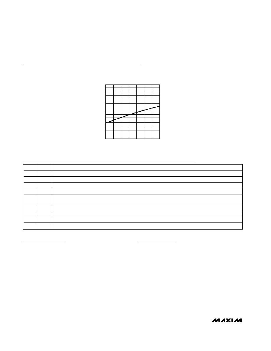
Typical Operating Characteristics
(T
A
= +25∞C, unless otherwise noted.)
0.1
2.0
2.5
3.5
4.0
5.5
4.5
5.0
3.0
TIMEKEEPING CURRENT
vs. SUPPLY VOLTAGE
1.0
10.0
MAX6901 toc01
SUPPLY VOLTAGE (V)
SUPPLY CURRENT (
µ
A)
PIN
NAME
FUNCTION
1
SCLK
Serial Clock Input. 3-wire serial clock for I/O data transfers.
2
V
CC
Power-Supply Pin. Bypass V
CC
to GND with a 0.1µF capacitor.
3
X2
External 32.768kHz Crystal Connection
4
X1
External 32.768kHz Crystal Connection
5
32KHZ
Buffered Push-Pull 32.768kHz Output. When enabled, 32KHZ puts a buffered version of the timekeeping clock.
When disabled, 32KHZ is high impedance. The power-on reset (POR) default state of 32KHZ is enabled.
6
GND
Ground Connection
7
CS
Chip-Select Input. Active-high for valid data transfers.
8
I/O
Data Input/Output. 3-wire serial data input/output connection.
--
PAD
Ground
Pin Description
Clock Burst Mode
Accessing the Clock Burst register specifies burst-
mode operation. In this mode, multiple bytes are read
or written with a single Address/Command write. If the
Clock Burst register is accessed (BEh for Write and
BFh for Read), the first seven clock/calendar registers
(Seconds, Minutes, Hours, Date, Month, Day, and Year)
and the Control register, are consecutively read or writ-
ten, starting with the LSB of the Seconds register. When
writing to the clock registers in burst mode, all seven
registers must be written in order for the data to be
transferred (see Example: Setting the Clock with a
Burst Write).
RAM Burst Mode
Sending the RAM Burst Address/Command specifies
Burst-Mode operation. In this mode, the 31 RAM regis-
ters can be consecutively read or written, starting with
bit 0 of address C0h for Writes, and C1h for Reads.
Burst Read outputs all 31 registers of RAM. When writ-
ing to RAM in burst mode, it is not necessary to write all
31 bytes for the data to transfer; each complete byte
written is transferred to RAM. When reading from RAM,
data bits are output until all 31 bytes have been read,
or until CS is driven low.
Setting the Clock
Writing to the Timekeeping Registers
The Time and Date are set by writing to the timekeep-
ing registers (Seconds, Minutes, Hours, Date, Month,
Day, Year, and Century). During a write operation, an
input buffer accepts the new time data while the time-
keeping registers continue to increment normally,
based on the crystal counter. The buffer also keeps the
timekeeping registers from changing as the result of an
incomplete Write operation, and collision detection cir-
cuitry ensures that a time write does not occur coinci-
dent with a Seconds register increment. The updated
time data are loaded into the timekeeping registers on
the falling edge of CS, at the end of the 3-wire serial
Write operation. An incomplete Write operation aborts
the update procedure, and the contents of the input
buffer are discarded. The timekeeping registers reflect
the new time, beginning with the first Seconds register
increment after the falling edge of CS.
Although both Single Writes and Burst Writes are possi-
ble, the best way to write to the timekeeping registers is
with a Burst Write. With a Burst Write, main timekeeping
registers (Seconds, Minutes, Hours, Date, Month, Day,
Year), and the Control register are written sequentially
following the Address/Command byte. They must be
written as a group of eight registers, with 8 bits each,
for proper execution of the Burst Write function. All
seven timekeeping registers are simultaneously loaded
into the clock counters by the falling edge of CS, at the
end of the 3-wire serial Write operation. For a normal
burst data transfer, the worst-case error that can occur
between the actual time and the written time update is
1 second.
If Single Write operations are used to enter data into the
timekeeping registers, error checking is required. If the
Seconds register is not to be written, then begin by
reading the Seconds register and save it as initial-sec-
onds. Write to the required timekeeping registers and
MAX6901
3-Wire Serial RTC in a TDFN
_______________________________________________________________________________________
5
Figure 1. Oscillator Circuit Schematic
Rf
Rd
Cd
25pF
Cg
25pF
EXTERNAL
CRYSTAL
X1
X2
MAX6901
PARAMETER
SYMBOL
MIN
TYP
MAX
UNITS
Frequency
f
32.76
kHz
Equivalent Series Resistance (ESR)
R
s
40
60
k
Parallel Load Capacitance
C
L
11.2
12.5
13.7
pF
Q Factor
Q
40,000
60,000
Table 1. Acceptable Quartz Crystal Parameters