For pricing, delivery, and ordering information, please contact Maxim/Dallas Direct! at
1-888-629-4642, or visit Maxim's website at www.maxim-ic.com.
General Description
The MAX6901 evaluation system (EV system) consists
of a MAX6901 evaluation kit (EV kit) and a companion
Maxim SMBusTM interface board.
The MAX6901 EV kit is an assembled and tested PC
board that demonstrates the MAX6901 3-wire serial
real-time clock (RTC). This EV kit is intended to demon-
strate the functionality and features of the MAX6901
RTC. It is not designed to exercise the MAX6901 at its
maximum serial bus interface speed. A typical bus
interface speed is in the 90kHz range and depends
upon the operating system and computer used.
The Maxim SMBus interface board (MAXSMBus) allows
an IBM-compatible PC to use its parallel port to emulate
SPITM, 3-wire, and SMBus (2-wire) interfaces. Windows
Æ
95/98-compatible software provides a user-friendly
interface to exercise the features of the MAX6901.
(Note: Windows NT/2000 requires additional driver soft-
ware; contact the factory.) The program is menu driven
and offers a graphic interface with control buttons and
status display.
Order the complete EV system (MAX6901EVSYS) for
comprehensive evaluation of the MAX6901 using a PC.
Order the EV kit (MAX6901EVKIT) if the MAXSMBus
module has already been purchased with a previous
Maxim EV system, or for custom use in other µC-based
systems.
Features
o Proven PC Board Layout
o Low-Voltage Operation
o Supply-Current Monitoring
o Fully Assembled and Tested
o Easy-to-Use Menu-Driven Software
o Includes: Windows 95/98-Compatible Software
(3.5in Floppy Disk) Demo PC Board
Evaluates: MAX6901
MAX6901 Evaluation System/Evaluation Kit
________________________________________________________________ Maxim Integrated Products
1
19-2148; Rev 0; 8/01
Component Suppliers
Ordering Information
SUPPLIER
PHONE
FAX
Murata
770-436-1300
770-436-3030
Taiyo Yuden
800-348-2496
847-925-0899
TDK
847-803-6100
847-390-4405
MAX6901EV Component List
DESIGNATION
QTY
DESCRIPTION
C1, C2, C3,
C6
4
0.1µF, 16V X7R ceramic
capacitors (0603)
Taiyo Yuden EMK107BJ104KA or
Murata GRM39X7R104K016 or
TDK C1608X7R1C104K
C4, C5
2
10µF, 35V capacitors
Al Electrolytic
J1
1
2
10 right-angle female
receptacle
JU1, JU2
2
2-pin headers
JU3≠JU6
0
Not installed
R1
1
49.9k
±1% resistor
R2
1
470k
±5% resistor
R3
1
100k
±5% resistor
U1
1
MAX6901EKA (8-pin SOT23)
real-time clock
U2
1
MAX1840EUB (10-pin µMAX)
level translator
U3
1
MAX1615EUK (5-pin SOT23)
linear voltage regulator
Y1
1
32.768kHz, 12.5pF quartz crystal
Y2
0
Not installed
PART
TEMP. RANGE
INTERFACE TYPE
MAX6901EVKIT
0∞C to +70∞C
User supplied
MAX6901EVSYS
0∞C to +70∞C
MAXSMBus
SMBus is a trademark of Intel Corp.
SPI is a trademark of Motorola, Inc.
Windows is a registered trademark of Microsoft Corp.
Note: The MAX6901 EV kit software is provided with the
MAX6901EVKIT. However, to use the software, the MAXSMBus
board is required to interface the EV kit to the computer.
Note: Please indicate you are using the MAX6901 when contact-
ing these manufacturers.
MAX6901EVSYS
Component List
PART
QTY
DESCRIPTION
MAX6901EVKIT
1
MAX6901 EV kit
MAXSMBUS
1
Interface board

Evaluates: MAX6901
MAX6901 Evaluation System/Evaluation Kit
2
_______________________________________________________________________________________
Quick Start
Required Equipment
Before you begin, the following equipment is needed:
∑
Maxim MAX6901EVKIT and MAXSMBus interface
board
∑
12VDC power supply (Any supply voltage between
+9V and +15V is acceptable.)
∑
Computer running Windows 95 or 98
∑
Spare parallel port
∑
25-pin I/O extension cable
Procedure
1) Carefully connect the boards by aligning the 20-pin
connector of the MAX6901 EV kit with the 20-pin
header of the MAXSMBus interface board. Gently
press them together. The two boards should be flush
against each other.
Do not turn on the power until all connections are
made.
2) Connect the 25-pin I/O extension cable from the
computer's parallel port to the MAXSMBus board.
The EV kit software uses a loopback connection to
confirm that the correct port has been selected.
3) Install the EV system software on your computer by
running the INSTALL.EXE program on the floppy
disk. The program files are copied and icons are
created for them in the Windows Start menu.
4) Ensure that the jumper settings are in the default
position (Table 1).
5) Connect the 12VDC power supply to the
MAXSMBus board between POS9 and GND.
Voltage for the MAX6901 ICs comes from the
MAXSMBus board.
6) Start the program by opening its icon in the Start
menu.
7) Click on the Set from Computer's Clock button to
write the current time of day into the MAX6901.
8) Observe the difference between the computer's time
and the MAX6901 time. The offset is calculated by
Offset = RTC time - PC time. In general, the RTC
keeps more accurate time than the PC. To determine
long-term accuracy of the RTC, it must be set by and
checked against an accurate time source. The easi-
est way to do this using the MAX6901 EV software is
to use an Internet time service to set the PC clock and
then set the RTC from the PC clock. This Internet time
service can then be used to accurately update the PC
clock regularly for an accurate comparison of the
RTC against a known time standard. The National
Institute of Standards and Technology (NIST) offers
such an Internet time service without charge
(http://www.boulder.nist.gov/timefreq/service/its.htm).
Note: The MAX6901EVSYS may be unplugged from the
parallel port for long-term drift testing.
Detailed Description of
Hardware
The MAX6901 (U1) is a real-time clock with RAM. The
MAX1840 level translator (U2) is not required for normal
operation of the MAX6901, but allows operation at supply
voltages down to +2V, while still communicating with the
MAXSMBus board, which is using +5V logic levels. See
Figure 7 and refer to the MAX6901 data sheet.
Measuring Timekeeping Supply Current
The MAX6901 is in standby mode whenever no com-
mands are being sent. To measure the timekeeping
supply current drawn in standby mode, first ensure that
the main screen's Cyclic Burst Read checkbox is not
checked, disable the 32kHz output by checking the
32kHz Disable checkbox, remove the shunt from JU2,
and measure the voltage across R1. A voltage drop of
10mV represents 200nA of timekeeping supply current.
For active bus operation (serial bus activity), replace
shunt JU2 to prevent excessive voltage drop across
resistor R1.
Surface-Mount Crystal
The EV kit comes with a 1.1mm cylindrical tuning fork
crystal; however, the PC board layout accommodates an
optional surface-mount crystal. Only one crystal may be
used.
Table 1. Jumper Functions
JUMPER
POSITION
FUNCTION
*Closed
V
L
= +5V
JU1
Open
User-supplied V
L
+5V
*Closed
Supply current-sensing resistor
R1 is shorted, enabling
communication with the RTC.
JU2
Open
Timekeeping supply current can
be estimated by measuring
voltage across R1.
Communication is not possible in
this state.
*Asterisk indicates default configuration.

MAXSMBus Connector
The MAXSMBus board connects to the MAX6901 EV kit
in accordance with Table 2.
Evaluation of the MAX6901 at
a Lower Voltage
To evaluate the MAX6901 at a lower voltage, remove
the shunt from jumper JU1 and apply the desired volt-
age (+2V to +5V) to the VL pad.
EV Kit Stand-Alone
The MAX6901 EV kit can be connected to a different 3-
wire interface with or without level translation.
To connect with level translation, use the pads labeled
X_I/O, X_SCLK, and X_CS. Cut the trace-shorting jumper
JU6 and connect the 3-wire interface logic voltage to the
VCC pad. Remove the shunt from JU1 and apply the
desired voltage for the MAX6901 to the VL pad.
To connect without level translation, cut the traces short-
ing JU3, JU4, and JU5 and use the pads labeled I/O,
SCLK, and CS. Remove the shunt from JU1 and connect
the 3-wire interface logic-voltage to the VL pad.
Troubleshooting
Problem: Unable to communicate while measuring
supply current.
JU2 must be closed to enable communication.
Problem: Initial date POR value of RTC is 01-JAN-2070.
RTC evaluation software was started. RTC time was set
from computer clock. RTC was powered down. RTC
evaluation software remained running and then RTC
was powered back up. RTC evaluation software only
reads the Century register when time is set from the
computer clock or when the software is initially
launched. Stop Cyclic Burst Read. Do a single read of
the Century register. Continue by starting the Cyclic
Burst Read.
Detailed Description
of Software
The evaluation software provides access to all regis-
ters. The main timekeeping registers appear in the
main screen, with other screens accessible from the
View menu. To write to a single register, click on the
appropriate register select button, set the desired
value, and then click the Write button. To read a regis-
ter, click on the appropriate register select button, and
then click the Read button. Cyclic Burst Read should
be disabled before a read or write to a single register.
Main Screen
The Read button reads the most recently selected time-
keeping register. The Write button writes the most
recently selected timekeeping register. The Burst Read
button performs a Burst Read from the timekeeping
registers (except Century). The Burst Write button per-
forms a Burst Write to the timekeeping registers (except
Century). The Set from Computer's Clock button writes
the PC's time into the MAX6901. The Cyclic Burst Read
checkbox tells the software to perform a Burst Read
from the timekeeping registers, at a rate of approxi-
mately four times per second. Updates are shown in
the register display, along with the difference between
MAX6901 time and the host PC's time. Note: Cyclic
Burst Read should be disabled before a read or write to
a single register. Figure 1 shows the main screen.
The Hour register setting can be switched from 12hr
format to 24hr format by clicking the -->24 button.
Checking the 32kHz Disable checkbox disables the
32kHz output (pin 5) on the MAX6901. A checkmark cor-
responds to a logic 1 for bit 7 of the Seconds register.
Evaluates: MAX6901
MAX6901 Evaluation System/Evaluation Kit
_______________________________________________________________________________________
3
Table 2. MAXSMBus Connector Signals
PIN
CONNECTOR P1 ON
MAXSMBus BOARD
CONNECTOR J1 ON
MAX6901 EV KIT
1
+5V
No connection
2
GND
Ground
3
SDA
X_I/O
4
GND
Ground
5
GND
Ground
6
GND
Ground
7
SCL
X_SCLK
8
GND
Ground
9
SMBSUS
X_CS
10
GND
Ground
11
ALERT
No connection
12
GND
Ground
13
ALERT2
No connection
14
GND
Ground
15
OUTA
No connection
16
GND
Ground
17
OUTB
No connection
18
GND
Ground
19
GND
Ground
20
RAW PWR
+9V
Note: Odd-numbered pins are on the outer row. Even-num-
bered pins are on the inner row.

Evaluates: MAX6901
RAM Screen
The Single Read button reads the most recently select-
ed RAM location. The Single Write button writes the
most recently selected RAM location. The Burst Read
button performs a Burst Read from the entire RAM. The
Burst Write button performs a Burst Write to the RAM.
Normally, all 31 locations are read, but the Burst Write
length can be reduced. The Burst Write always begins
with RAM location 0. The Preset Data button performs a
Burst Write to the RAM, setting all data to the same
value. Note: Cyclic Burst Read should be disabled
before reading or writing to RAM. Figure 2 is the RAM
screen.
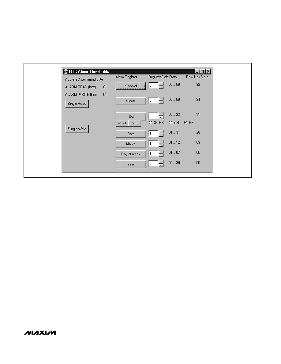
Alarm Thresholds Screen
The Read button reads the most recently selected
alarm threshold register. The Write button writes the
most recently selected alarm threshold register.
The Hour register setting can be switched from 12hr
format to 24hr format by clicking the -->24 button.
Note: Cyclic Burst Read should be disabled before a
read or write to a single register. Figure 3 is the Alarm
Thresholds screen.
MAX6901 Evaluation System/Evaluation Kit
4
_______________________________________________________________________________________
Figure 2. RAM Screen
Figure 1. Main Screen
Setup Screen
Each setup register is represented by a group of eight
checkboxes, one for each bit. A checkmark indicates
that the corresponding bit is a logic 1. The Read button
updates the most recently selected setup register's
checkboxes. The Write button writes the most recently
selected setup register. Note: Cyclic Burst Read
should be disabled before a read or write to a single
register. Figure 4 is the Setup screen.
Auxiliary Functions
SPI/3-Wire Diagnostic
The transition from evaluation to custom software devel-
opment requires access to the low-level interface.
Access the SPI/3-wire diagnostic from the main
screen's View menu. The SPI/3-Wire Diagnostic screen
allows you to send SPI or 3-wire commands, or manipu-
late the parallel port pins directly. Each of the 25 paral-
lel port pins is represented by a checkbox. A check-
mark means that the corresponding pin is at a logic
high level. Pins that are inputs to the PC are grayed.
The Bit Banging SPI Diagnostic transmits data using
synchronous serial format (similar to Motorola's
68HC11 SPI interface). The SPI interface sends and
receives data simultaneously on separate pins. Parallel
port pin 2 drives the SCLK, pin 1 drives DIN, pin 4 dri-
ves CS, and pin 11 senses DOUT.
When the software is communicating through the
MAXSMBus board DOUT, CS, and SCLK are inverted.
DIN is not inverted.
The signals come out of the MAXSMBus at connector
P1; DOUT is pin 3, CS is pin 9, SCLK is pin 7, and DIN
is pin 15.
The 3-wire interface uses a bidirectional data pin. The
least-significant bit (LSB) is transmitted first, and (CPOL
= 1, CPHA = 0) mode is used. Parallel port pin 2 drives
SCLK, pin 11 drives I/O, and pin 4 drives CS.
When the software is communicating through the
MAXSMBus board SCLK, I/O and CS are inverted.
The signals come out of the MAXSMBus at connector
P1; SCLK is pin 7, CS is pin 9, and I/O is pin 3.
When using this software, the data is relative to the par-
allel port. However, there are checkboxes that allow the
signals to be inverted to accommodate the
MAXSMBus board. Note: Disable Cyclic Burst Read
when using the SPI/3-wire diagnostic utility. Figure 5 is
the SPI/3-Wire Diagnostic screen.
Evaluates: MAX6901
MAX6901 Evaluation System/Evaluation Kit
_______________________________________________________________________________________
5
Figure 3. Alarm Thresholds Screen