 | ÐлекÑÑоннÑй компоненÑ: MAX7311 | СкаÑаÑÑ:  PDF PDF  ZIP ZIP |
Äîêóìåíòàöèÿ è îïèñàíèÿ www.docs.chipfind.ru
General Description
The MAX7311 2-wire-interfaced expander provides 16-bit
parallel input/output (I/O) port expansion for SMBusTM
and I
2
CTM applications. The MAX7311 consists of input
port registers, output port registers, polarity inversion reg-
isters, configuration registers, a bus timeout register, and
an I
2
C-compatible serial interface logic compatible with
SMBus. The system master can invert the MAX7311 input
data by writing to the active-high polarity inversion regis-
ter. The system master can enable or disable bus timeout
by writing to the bus timeout register.
Any of the 16 I/O ports can be configured as an input or
output. A power-on reset (POR) initializes the 16 I/Os
as inputs. Three address select pins configure one of
64 slave ID addresses.
The MAX7311 supports hot insertion. All port pins, the
INT output, SDA, SCL and the slave address inputs
AD02 remain high impedance in power down (V+ =
0V) with up to 6V asserted upon them.
The MAX7311 is available in 24-pin SO, SSOP, TSSOP,
and thin QFN packages and is specified over the -40°C
to +125°C automotive temperature range.
For applications requiring I/Os without pullup resistors,
refer to the MAX7312 data sheet.
Applications
Servers
RAID Systems
Industrial Control
Medical Equipment
PLCs
Instrumentation and Test Measurement
Features
400kbps I
2
C-Compatible Serial Interface
2V to 5.5V Operation
5V Overvoltage Tolerant I/Os
Supports Hot Insertion
16 I/O Pins that Default to Inputs on Power-Up
100k Pullup on Each I/O
Open-Drain Interrupt Output (INT)
Bus Timeout for Lock-Up-Free Operation
Noise Filter on SCL / SDA Inputs
64 Slave ID Addresses Available
Low Standby Current (2.9µA typ)
Polarity Inversion
4mm
4mm, 0.8mm Thin QFN Package
-40°C to +125°C Operation
MAX7311
2-Wire-Interfaced 16-Bit I/O Port Expander
with Interrupt and Hot-Insertion Protection
________________________________________________________________ Maxim Integrated Products
1
Ordering Information
19-2747; Rev 4; 4/05
For pricing, delivery, and ordering information, please contact Maxim/Dallas Direct! at
1-888-629-4642, or visit Maxim's website at www.maxim-ic.com.
SMBus is a trademark of Intel Corp.
Purchase of I
2
C components of Maxim Integrated Products, Inc.
or one of its sublicensed Associated Companies, conveys a
license under the Phillips I
2
C Patent Rights to use these compo-
nents in an I
2
C system, provided that the system conforms to the
I
2
C Standard Specification as defined by Phillips.
PART
TEMP RANGE
PIN-PACKAGE
PKG
CODE
MAX7311AWG
-40°C to +125°C 24 Wide SO
--
MAX7311AAG
-40°C to +125°C 24 SSOP
--
MAX7311ATG
-40°C to +125°C
24 Thin QFN
(4mm
4mm)
T2444-4
MAX7311AUG
-40°C to +125°C 24 TSSOP
--
TOP VIEW
24
23
22
21
20
19
18
17
1
2
3
4
5
6
7
8
V+
SDA
SCL
AD0
I/O0
AD2
AD1
I/O15
I/O14
I/O13
I/O12
I/O4
I/O3
I/O2
I/O1
16
15
14
13
9
10
11
12
I/O11
I/O10
I/O9
I/O8
GND
I/O7
I/O6
I/O5
TSSOP/SSOP/SO
MAX7311
INT
THIN QFN
MAX7311ATG
19
20
21
22
1
2
3
4
5
6
18
17
16
15
14
13
23
24
12
11
10
9
8
7
SCL
V+
SDA
INT
AD2
I/O0
I/O1
I/O2
I/O3
I/O4
I/O5
AD0
I/O15
I/O13
I/O12
I/O11
AD1
I/O10
I/O8
I/O9
GND
I/O6
I/O7
I/O14
Pin Configurations
MAX7311
2-Wire-Interfaced 16-Bit I/O Port Expander
with Interrupt and Hot-Insertion Protection
2
_______________________________________________________________________________________
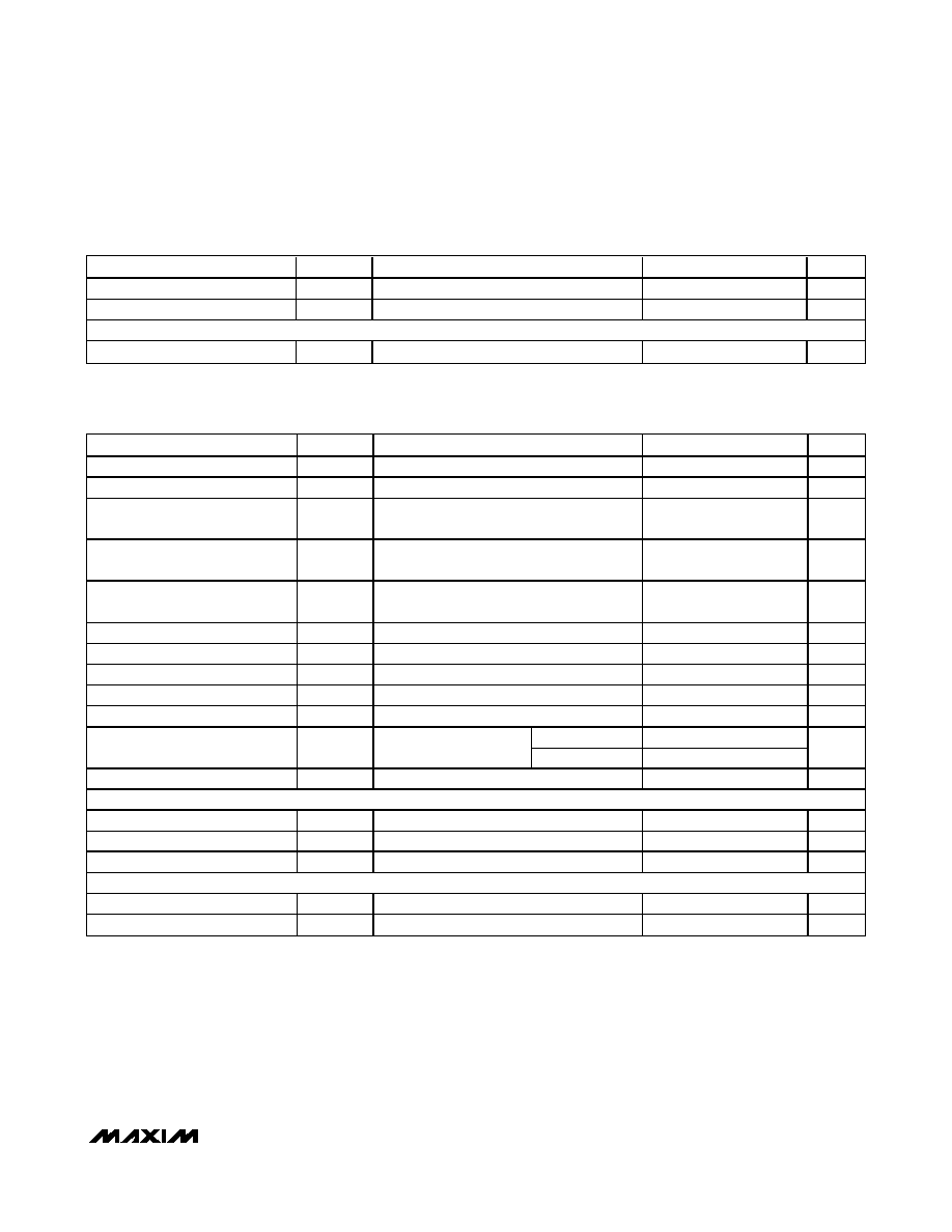
ABSOLUTE MAXIMUM RATINGS
DC ELECTRICAL CHARACTERISTICS
(V+ = 2V to 5.5V, T
A
= -40°C to +125°C, unless otherwise noted. Typical values are at V+ = 3.3V, T
A
= +25°C.) (Note 1)
Stresses beyond those listed under "Absolute Maximum Ratings" may cause permanent damage to the device. These are stress ratings only, and functional
operation of the device at these or any other conditions beyond those indicated in the operational sections of the specifications is not implied. Exposure to
absolute maximum rating conditions for extended periods may affect device reliability.
V
+
to GND ................................................................-0.3V to +6V
I/O0I/O15 as Inputs ....................................(GND - 0.3V) to +6V
SCL, SDA, AD0, AD1, AD2, INT...................(GND - 0.3V) to +6V
Maximum V
+
Current ......................................................+250mA
Maximum GND Current ...................................................-250mA
DC Input Current on I/O0I/O15 .......................................±20mA
DC Output Current on I/O0I/O15 ....................................±80mA
Continuous Power Dissipation (T
A
= +70°C)
24-Pin Wide SO (derate 11.8mW/°C above +70°C) ....941mW
24-Pin SSOP (derate 8.0mW/°C above +70°C) ...........640mW
24-Pin TSSOP (derate 12.2mW/°C above +70°C) .......975mW
24-Pin Thin QFN (derate 20.8mW/°C above +70°C) .1668mW
Operating Temperature Range .........................-40°C to +125°C
Junction Temperature ......................................................+150°C
Storage Temperature Range .............................-65°C to +150°C
Lead Temperature (soldering, 10s) .................................+300°C
PARAMETER
SYM B O L CONDITIONS
MIN
TYP
MAX
UNITS
Supply Voltage
V
+
2
5.5
V
V
+
= 2V
23
35
V
+
= 3.3V
43
60
Supply Current
I
+
All I/Os unloaded,
f
SCL
= 400kHz
V
+
= 5.5V
80
120
µA
V
+
= 2V
2.3
11
V
+
= 3.3V
2.9
12
Standby Current
I
STBY
All I/Os unloaded,
f
SCL
= 0
V
+
= 5.5V
3.8
15.5
µA
Power-On Reset Voltage
V
POR
1.4
1.7
V
SCL, SDA
Input Voltage Low
V
IL
0.3
V
+
V
Input Voltage High
V
IH
0.7
V
+
V
Low-Level Output Voltage
V
OL
I
SINK
= 6mA
0.4
V
Leakage Current
I
L
-1
+1
µA
Input Capacitance
10
pF
I/O_
Input Voltage Low
V
IL
0.8
V
Input Voltage High
V
IH
1.8
V
Input Leakage Current
T
A
= -40°C to +85°C; includes internal
pullup current, V
IO
= V
+
1
µA
Internal Pullup Current
T
A
= -40°C to +85°C, V
IO
= 0
34
100
µA
V
+
= 2V, V
OL
= 0.5V
8.5
17
V
+
= 3.3V, V
OL
= 0.5V
17
32
Low-Level Output Current
I
SINK
V
+
= 5V, V
OL
= 0.5V
43
mA
V
+
= 3.3V, V
OH
= 2.4V
29
41
High Output Current
I
SOURCE
V
+
= 5V, V
OH
= 4.5V
31
mA
AD0, AD1, AD2
Input Voltage Low
V
IL
0.3
V
+
V
Input Voltage High
V
IH
0.7
V
+
V
MAX7311
2-Wire-Interfaced 16-Bit I/O Port Expander
with Interrupt and Hot-Insertion Protection
_______________________________________________________________________________________
3
Note 1: All parameters are 100% production tested at T
A
= +25°C. Specifications over temperature are guaranteed by design.
Note 2: Minimum SCL clock frequency is limited by the MAX7311 bus timeout feature, which resets the serial bus interface if either
SDA or SCL is held low for a minimum of 25ms. Disable bus timeout feature for DC operation.
Note 3: A master device must internally provide a hold time of at least 300ns for the SDA signal (referred to the V
IL
of the SCL
signal) in order to bridge the undefined region SCL's falling edge.
Note 4: C
B
= total capacitance of one bus line in pF.
Note 5: The maximum t
F
for the SDA and SCL bus lines is specified at 300ns. The maximum fall time for the SDA output stage t
F
is
specified at 250ns. This allows series protection resistors to be connected between the SDA and SCL pins and the
SDA/SCL bus lines without exceeding the maximum specified t
F
.
Note 6: Input filters on the SDA and SCL inputs suppress noise spikes less than 50ns.
DC ELECTRICAL CHARACTERISTICS (continued)
(V+ = 2V to 5.5V, T
A
= -40°C to +125°C, unless otherwise noted. Typical values are at V+ = 3.3V, T
A
= +25°C.) (Note 1)
PARAMETER
SYM B O L CONDITIONS
MIN
TYP
MAX
UNITS
Leakage Current
-1
+1
µA
Input Capacitance
4
pF
INT
Low-Level Output Current
I
OL
V
OL
= 0.4V
6
mA
AC ELECTRICAL CHARACTERISTICS
(V+ = 2V to 5.5V, T
A
= -40°C to +125°C, unless otherwise noted.) (Note 1)
PARAMETER
SYM B O L CONDITIONS
MIN
TYP
MAX
UNITS
SCL Clock Frequency
f
SCL
(Note 2)
400
kHz
Bus Timeout
t
TIMEOUT
29
61
ms
Bus Free Time Between STOP
and START Conditions
t
BUF
Figure 2
1.3
µs
Hold Time (Repeated) START
Condition
t
HD,STA
Figure 2
0.6
µs
Repeated START Condition
Setup Time
t
SU,STA
Figure 2
0.6
µs
STOP Condition Setup Time
t
SU,STO
Figure 2
0.6
µs
Data Hold Time
t
HD,DAT
Figure 2 (Note 3)
0.9
µs
Data Setup Time
t
SU,DAT
Figure 2
100
ns
SCL Low Period
t
LOW
Figure 2
1.3
µs
SCL High Period
t
HIGH
Figure 2
0.7
µs
V+ < 3.3V
500
SDA Fall Time
t
F
Figure 2 (Notes 4, 5)
V+
3.3V
250
ns
Pulse Width of Spike Suppressed
t
SP
(Note 6)
50
ns
PORT TIMING
Output Data Valid
t
PV
Figure 7
3
µs
Input Data Setup Time
27
µs
Input Data Hold Time
0
µs
INTERRUPT TIMING
Interrupt Valid
t
IV
Figure 9
30.5
µs
Interrupt Reset
t
IR
Figure 9
2
µs
MAX7311
2-Wire-Interfaced 16-Bit I/O Port Expander
with Interrupt and Hot-Insertion Protection
4
_______________________________________________________________________________________
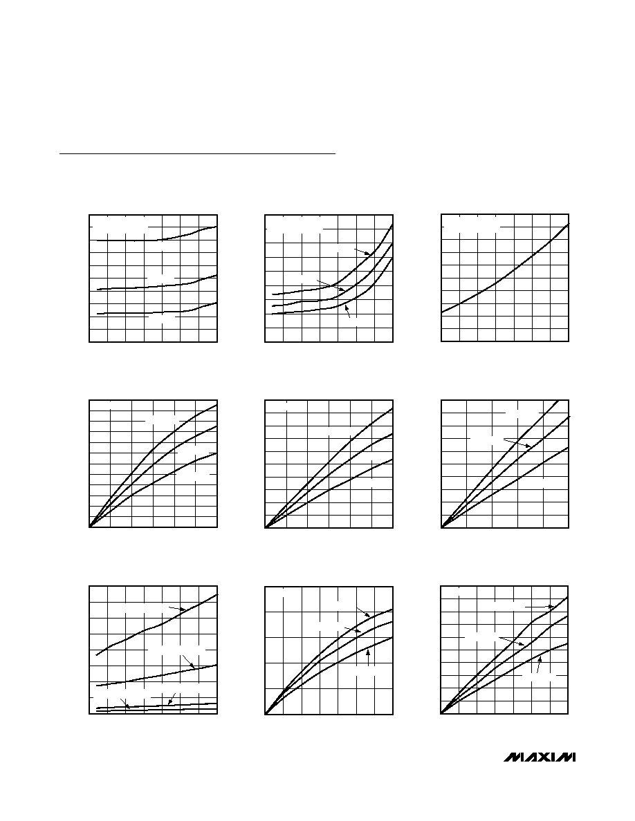
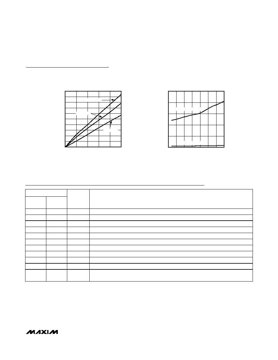
Typical Operating Characteristics
(T
A
= +25°C, unless otherwise noted.)
SUPPLY CURRENT
vs. TEMPERATURE
MAX7311 toc01
TEMPERATURE (
°C)
SUPPLY CURRENT (
µ
A)
100
75
25
50
0
-25
10
20
30
40
50
60
70
80
90
100
0
-50
125
f
SCL
= 400kHz
ALL I/Os UNLOADED
V
+
= 3.3V
V
+
= 5V
V
+
= 2V
STANDBY SUPPLY CURRENT
vs. TEMPERATURE
MAX7311 toc02
TEMPERATURE (
°C)
SUPPLY CURRENT (
µ
A)
100
75
25
50
0
-25
1
2
3
4
5
6
7
8
9
0
-50
125
SCL = V
+
ALL I/Os UNLOADED
V
+
= 3.3V
V
+
= 5V
V
+
= 2V
SUPPLY CURRENT
vs. SUPPLY VOLTAGE
MAX7311 toc03
SUPPLY VOLTAGE (V)
SUPPLY CURRENT (
µ
A)
5.0
4.5
3.5
4.0
3.0
2.5
10
20
30
40
50
60
70
80
90
100
0
2.0
5.5
f
SCL
= 400kHz
ALL I/Os UNLOADED
I/O SINK CURRENT
vs. OUTPUT LOW VOLTAGE
MAX7311 toc04
V
OL
(V)
I
SINK
(mA)
0.5
0.4
0.3
0.2
0.1
2
4
6
8
10
12
14
16
18
20
22
24
0
0
0.6
V
+
= 2V
T
A
= +125
°C
T
A
= +25
°C
T
A
= -40
°C
I/O SINK CURRENT
vs. OUTPUT LOW VOLTAGE
MAX7311 toc05
V
OL
(V)
I
SINK
(mA)
0.5
0.4
0.3
0.2
0.1
5
10
15
20
25
30
35
40
45
50
0
0
0.6
V
+
= 3.3V
T
A
= +125
°C
T
A
= -40
°C
T
A
= +25
°C
I/O SINK CURRENT
vs. OUTPUT LOW VOLTAGE
MAX7311 toc06
V
OL
(V)
I
SINK
(mA)
0.4
0.3
0.2
0.1
5
10
15
20
25
30
35
40
45
50
0
0
0.5
V
+
= 5V
T
A
= +125
°C
T
A
= -40
°C
T
A
= +25
°C
I/O OUTPUT LOW VOLTAGE
vs. TEMPERATURE
MAX7311 toc07
TEMPERATURE (
°C)
V
OL
(mV)
100
75
-25
0
25
50
50
100
150
200
250
300
350
400
0
-50
125
V
+
= 5V, I
SINK
= 10mA
V
+
= 2V, I
SINK
= 10mA
V
+
= 2V, I
SINK
= 1mA
V
+
= 5V, I
SINK
= 1mA
I/O SOURCE CURRENT
vs. OUTPUT HIGH VOLTAGE
MAX7311 toc08
V
+
- V
OH
(V)
I
SOURCE
(mA)
0.6
0.5
0.4
0.3
0.2
0.1
5
10
15
20
25
0
0
0.7
V
+
= 2V
T
A
= +125
°C
T
A
= +25
°C
T
A
= -40
°C
I/O SOURCE CURRENT
vs. OUTPUT HIGH VOLTAGE
MAX7311 toc09
V
+
- V
OH
(V)
I
SOURCE
(mA)
0.6
0.5
0.3
0.4
0.2
0.1
5
10
15
20
25
30
35
40
45
50
0
0
0.7
V
+
= 3.3V
T
A
= +125
°C
T
A
= +25
°C
T
A
= -40
°C
MAX7311
2-Wire-Interfaced 16-Bit I/O Port Expander
with Interrupt and Hot-Insertion Protection
_______________________________________________________________________________________
5
Pin Description
Typical Operating Characteristics (continued)
(T
A
= +25°C, unless otherwise noted.)
I/O SOURCE CURRENT
vs. OUTPUT HIGH VOLTAGE
MAX7311 toc10
V
+
- V
OH
(V)
I
SOURCE
(mA)
0.6
0.5
0.3
0.4
0.2
0.1
5
10
15
20
25
30
35
40
45
50
0
0
V
+
= 5V
T
A
= +125
°C
T
A
= +25
°C
T
A
= -40
°C
I/O HIGH VOLTAGE vs. TEMPERATURE
MAX7311 toc11
TEMPERATURE (
°C)
V
+
- V
OH
(V)
100
75
50
25
0
-25
100
200
300
400
500
0
-50
125
V
+
= 5V, I
SOURCE
= 10mA
V
+
= 2V, I
SOURCE
= 10mA
PIN
TSSOP/
SSOP/SO
THIN
QFN
NAME
FUNCTION
1
22
INT
Interrupt Output (Open Drain)
2
23
AD1
Address Input 1
3
24
AD2
Address Input 2
411
18
I/O0I/O7
Input/Output Port 1
12
9
GND
Supply Ground
1320
1017
I/O8I/O15
Input/Output Port 2
21
18
AD0
Address Input 0
22
19
SCL
Serial Clock Line
23
20
SDA
Serial Data Line
24
21
V
+
Supply Voltage. Bypass with a 0.047µF capacitor to GND.
--
PAD
Exposed
pad
Exposed Pad on Package Underside. Connect to GND.