 | ÐлекÑÑоннÑй компоненÑ: MAX7314 | СкаÑаÑÑ:  PDF PDF  ZIP ZIP |
Äîêóìåíòàöèÿ è îïèñàíèÿ www.docs.chipfind.ru
General Description
The MAX7314 I
2
CTM-compatible serial interfaced periph-
eral provides microprocessors with 16 I/O ports plus one
output-only port and one input-only port. Each I/O port
can be individually configured as either an open-drain
current-sinking output rated at 50mA and 5.5V, or a logic
input with transition detection. The output-only port can
be assigned as an interrupt output for transition detec-
tion. The outputs are capable of driving LEDs, or provid-
ing logic outputs with external resistive pullup up to 5.5V.
Eight-bit PWM current control is built in for all 17 output
ports. A 4-bit global control applies to all LED outputs
and provides coarse adjustment of current from fully off
to fully on with 14 intensity steps in between. Each out-
put has an individual 4-bit control, which further divides
the globally set current into 16 more steps.
Alternatively, the current control can be configured as a
single 8-bit control that sets all outputs at once.
Each output has independent blink timing with two blink
phases. All LEDs can be individually set to be on or off
during either blink phase, or to ignore the blink control.
The blink period is controlled by a clock input (up to 1kHz)
on BLINK or by a register. The BLINK input can also be
used as a logic control to turn the LEDs on and off, or as a
general-purpose input.
The MAX7314 supports hot insertion. All port pins, the
INT output, SDA, SCL, RST, BLINK, and the slave
address input ADO remain high impedance in power-
down (V+ = 0V) with up to 6V asserted upon them.
The MAX7314 is controlled through a 2-wire serial inter-
face, and uses four-level logic to allow four I
2
C
addresses from only one select pin.
Applications
LCD Backlights
LED Status Indication
Relay Drivers
Keypad Backlights
RGB LED Drivers
System I/O Ports
Features
400kbps, 2-Wire Serial Interface, 5.5V Tolerant
2V to 3.6V Operation
Overall 8-Bit PWM LED Intensity Control
Global 16-Step Intensity Control
Individual 16-Step Intensity Controls
2-Phase LED Blinking
50mA Maximum Port Output Current
Supports Hot Insertion
Outputs are 5.5V-Rated Open Drain
Inputs are Overvoltage Protected to 5.5V
Transition Detection with Interrupt Output
1.2µA (typ), 3.6µA (max) Operating Current
Small 4mm x 4mm, Thin QFN Package
-40°C to +125°C Temperature Range
MAX7314
18-Port GPIO with LED Intensity Control,
Interrupt, and Hot-Insertion Protection
________________________________________________________________ Maxim Integrated Products
1
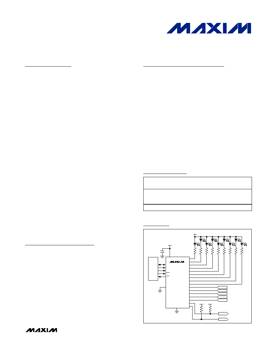
MAX7314
P8
P10
P0
P1
P2
P3
P4
P5
P6
P7
V+
3.3V
µC
SDA
SDA
AD0
3.3V
5V
P11
P12
P13
P14
P15
SCL
SCL
BLINK
I/O
RST
I/O
P9
OUTPUT
OUTPUT
GND
5V
INPUT 1
INPUT 2
INPUT 3
INPUT 4
INPUT 5
0.047
µF
INT
INT/O16
Typical Application Circuit
19-3170; Rev 4; 4/05
For pricing, delivery, and ordering information, please contact Maxim/Dallas Direct! at
1-888-629-4642, or visit Maxim's website at www.maxim-ic.com.
Ordering Information
PART
TEMP RANGE
PIN-
PACKAGE
PKG
CODE
MAX7314ATG
-40
°C to +125°C
24 Thin QFN
4mm x 4mm
x 0.8mm
T2444-4
MAX7314AEG
-40
°C to +125°C 24 QSOP
--
Pin Configurations continued at end of data sheet.
I
2
C is a trademark of Philips Corp.
Purchase of I
2
C components from Maxim Integrated Products,
Inc., or one of its sublicensed Associated Companies, conveys a
license under the Philips I
2
C Patent Rights to use these compo-
nents in an I
2
C system, provided that the system conforms to the
I
2
C Standard Specification as defined by Philips.
MAX7314
18-Port GPIO with LED Intensity Control,
Interrupt, and Hot-Insertion Protection
2
_______________________________________________________________________________________
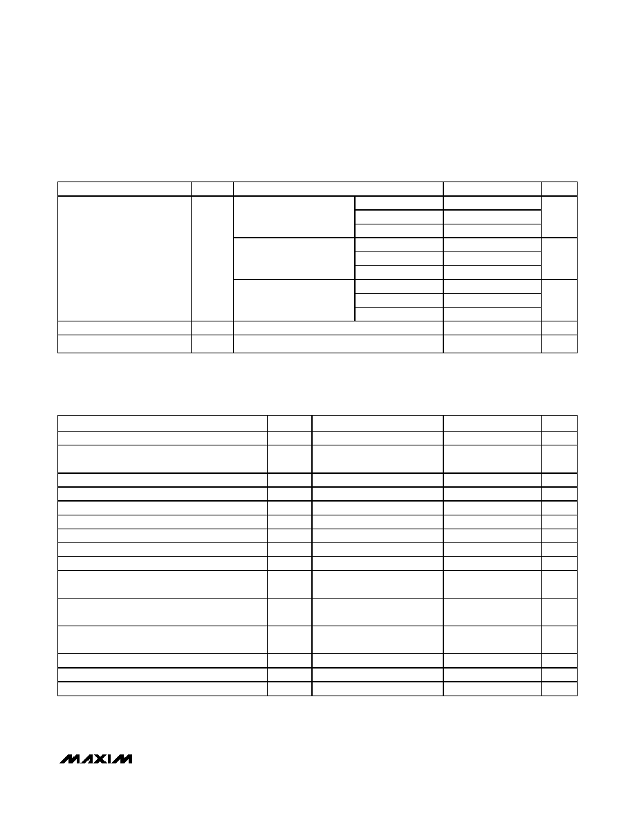
ABSOLUTE MAXIMUM RATINGS
Stresses beyond those listed under "Absolute Maximum Ratings" may cause permanent damage to the device. These are stress ratings only, and functional
operation of the device at these or any other conditions beyond those indicated in the operational sections of the specifications is not implied. Exposure to
absolute maximum rating conditions for extended periods may affect device reliability.
Voltage (with respect to GND)
V+ .............................................................................-0.3V to +4V
SCL, SDA, AD0, BLINK, RST, P0P15 .....................-0.3V to +6V
INT/O16 ...................................................................-0.3V to +8V
DC Current on P0P15, INT/O16 ........................................55mA
DC Current on SDA.............................................................10mA
Maximum GND Current ....................................................350mA
Continuous Power Dissipation (T
A
= +70°C)
24-Pin QSOP (derate 9.5mW/°C over +70°C)..............761mW
24-Pin QFN (derate 20.8mW/°C over +70°C) ............1666mW
Operating Temperature Range
(TMIN to TMAX) .............................................-40°C to +125°C
Junction Temperature ......................................................+150°C
Storage Temperature Range .............................-65°C to +150°C
Lead Temperature (soldering, 10s) .................................+300°C
ELECTRICAL CHARACTERISTICS
(Typical Operating Circuit, V+ = 2V to 3.6V, T
A
= T
MIN
to T
MAX
, unless otherwise noted. Typical values are at V+ = 3.3V, T
A
= +25°C.)
(Note 1)
PARAMETER
SYMBOL
CONDITIONS
MIN
TYP
MAX
UNITS
Operating Supply Voltage
V+
2
3.6
V
Output Load External Supply
Voltage
V
EXT
0
5.5
V
T
A
= +25°C
1.2
2.3
T
A
= -40°C to +85°C
2.8
Standby Current
(Interface Idle, PWM Disabled)
I
+
S C L and S D A at V + ; other
d i g i tal i np uts at V + or GN D ;
P WM i ntensi ty contr ol d i sab l ed
T
A
= T
MIN
to T
MAX
3.6
µA
T
A
= +25°C
8.5
15.1
T
A
= -40°C to +85°C
16.5
Supply Current
(Interface Idle, PWM Enabled)
I
+
S C L and S D A at V + ; other
d i g i tal i np uts at V + or GN D ;
P WM i ntensi ty contr ol d i sab l ed
T
A
= T
MIN
to T
MAX
17.2
µA
T
A
= +25°C
50
95.3
T
A
= -40°C to +85°C
99.2
Supply Current
(Interface Running, PWM
Disabled)
I
+
f
SCL
= 400kHz; other digital
inputs at V+ or GND; PWM
intensity control enabled
T
A
= T
MIN
to T
MAX
102.4
µA
T
A
= +25°C
57
110.2
T
A
= -40°C to +85°C
117.4
Supply Current
(Interface Running, PWM
Enabled)
I
+
f
SCL
= 400kHz; other digital
inputs at V+ or GND; PWM
intensity control enabled
T
A
= T
MIN
to T
MAX
122.1
µA
Input High Voltage
SDA, SCL, AD0, BLINK, P0P15
V
IH
0.7
x
V+
V
Input Low Voltage
SDA, SCL, AD0, BLINK, P0P15
V
IL
0.3
x
V+
V
Input Leakage Current
SDA, SCL, AD0, BLINK, P0P15
I
IH
, I
IL
0
input voltage 5.5V
-0.2
+0.2
µA
Input Capacitance
SDA, SCL, AD0, BLINK, P0P15
8
pF
MAX7314
18-Port GPIO with LED Intensity Control,
Interrupt, and Hot-Insertion Protection
_______________________________________________________________________________________
3
ELECTRICAL CHARACTERISTICS (continued)
(Typical Operating Circuit, V+ = 2V to 3.6V, T
A
= T
MIN
to T
MAX
, unless otherwise noted. Typical values are at V+ = 3.3V, T
A
= + 25°C.)
(Note 1)
PARAMETER
SYMBOL
CONDITIONS
MIN
TYP
MAX
UNITS
T
A
= +25°C
0.15
0.26
T
A
= -40°C to +85°C
0.3
V+ = 2V, I
SINK
= 20mA
T
A
= T
MIN
to T
MAX
0.32
V
T
A
= +25°C
0.13
0.23
T
A
= -40°C to +85°C
0.26
V+ = 2.5V, I
SINK
= 20mA
T
A
= T
MIN
to T
MAX
0.28
V
T
A
= +25°C
0.12
0.23
T
A
= -40°C to +85°C
0.24
Output Low Voltage
P0P15, INT/O16
V
OL
V+ = 3.3V, I
SINK
= 20mA
T
A
= T
MIN
to T
MAX
0.26
V
Output Low-Voltage SDA
V
OLSDA
I
SINK
= 6mA
0.4
V
PWM Clock Frequency
f
PWM
32
kHz
TIMING CHARACTERISTICS
(Typical Operating Circuit, V+ = 2V to 3.6V, T
A
= T
MIN
to T
MAX
, unless otherwise noted. Typical values are at V+ = 3.3V, T
A
= +25°C.)
(Note 1)
PARAMETER
SYMBOL
CONDITIONS
MIN
TYP
MAX
UNITS
Serial Clock Frequency
f
SCL
400
kHz
Bus Free Time Between a STOP and a START
Condition
t
BUF
1.3
µs
Hold Time, Repeated START Condition
t
HD, STA
0.6
µs
Repeated START Condition Setup Time
t
SU, STA
0.6
µs
STOP Condition Setup Time
t
SU, STO
0.6
µs
Data Hold Time
t
HD, DAT
(Note 2)
0.9
µs
Data Setup Time
t
SU, DAT
180
ns
SCL Clock Low Period
t
LOW
1.3
µs
SCL Clock High Period
t
HIGH
0.7
µs
Rise Time of Both SDA and SCL Signals, Receiving
t
R
(Notes 3, 4)
20 +
0.1C
b
300
ns
Fall Time of Both SDA and SCL Signals, Receiving
t
F
(Notes 3, 4)
20 +
0.1C
b
300
ns
Fall Time of SDA Transmitting
t
F.TX
(Notes 3, 5)
20 +
0.1C
b
250
ns
Pulse Width of Spike Suppressed
t
SP
(Note 6)
50
ns
Capacitive Load for Each Bus Line
C
b
(Note 3)
400
pF
RST Pulse Width
t
W
1
µs
MAX7314
18-Port GPIO with LED Intensity Control,
Interrupt, and Hot-Insertion Protection
4
_______________________________________________________________________________________
TIMING CHARACTERISTICS (continued)
(Typical Operating Circuit, V+ = 2V to 3.6V, T
A
= T
MIN
to T
MAX
, unless otherwise noted. Typical values are at V+ = 3.3V, T
A
= +25°C.)
(Note 1)
PARAMETER
SYMBOL
CONDITIONS
MIN
TYP
MAX
UNITS
Interrupt Valid
t
IV
Figure 10
6.5
µs
Interrupt Reset
t
IR
Figure 10
1
µs
Output Data Valid
t
DV
Figure 10
5
µs
Input Data Set-Up Time
t
DS
Figure 10
100
ns
Input Data Hold Time
t
DH
Figure 10
1
µs
Note 1: All parameters tested at T
A
= +25°C. Specifications over temperature are guaranteed by design.
Note 2: A master device must provide a hold time of at least 300ns for the SDA signal (referred to V
IL
of the SCL signal) to bridge
the undefined region of SCL's falling edge.
Note 3: Guaranteed by design.
Note 4: C
b
= total capacitance of one bus line in pF. t
R
and t
F
measured between 0.3 x V
DD
and 0.7 x V
DD
.
Note 5: I
SINK
6mA. C
b
= total capacitance of one bus line in pF. t
R
and t
F
measured between 0.3 x V
DD
and 0.7 x V
DD
.
Note 6: Input filters on the SDA and SCL inputs suppress noise spikes less than 50ns.
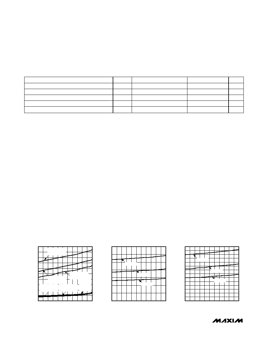
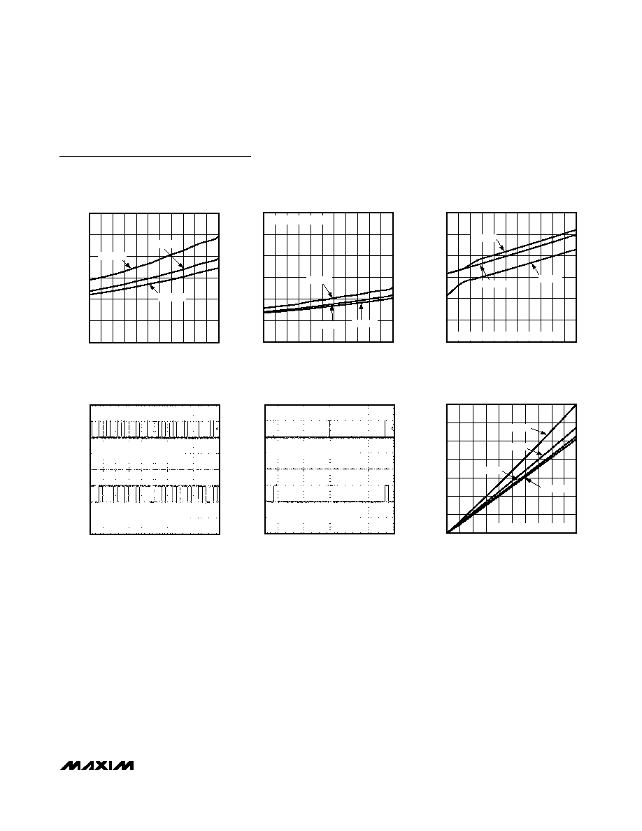
STANDBY CURRENT vs. TEMPERATURE
MAX7314 toc01
TEMPERATURE (
°C)
STANDBY CURRENT (
µ
A)
110
95
65 80
-10 5
20 35 50
-25
1
2
3
4
5
6
7
8
9
10
0
-40
125
V+ = 3.6V
PWM ENABLED
V+ = 2.7V
PWM ENABLED
V+ = 2V
PWM DISABLED
V+ = 2.7V
PWM DISABLED
V+ = 3.6V
PWM
DISABLED
V+ = 2V
PWM ENABLED
SUPPLY CURRENT vs. TEMPERATURE
(PWM DISABLED; f
SCL
= 400kHz)
MAX7314 toc02
TEMPERATURE (
°C)
SUPPLY CURRENT (
µ
A)
110
95
65 80
-10 5
20 35 50
-25
10
20
30
40
50
60
70
0
-40
125
V+ = 3.6V
V+ = 2.7V
V+ = 2V
5
10
15
20
25
30
35
40
45
50
55
60
65
70
0
SUPPLY CURRENT vs. TEMPERATURE
(PWM ENABLED; f
SCL
= 400kHz)
MAX7314 toc03
TEMPERATURE (
°C)
SUPPLY CURRENT (
µ
A)
110
95
65 80
-10 5
20 35 50
-25
-40
125
V+ = 3.6V
V+ = 2.7V
V+ = 2V
__________________________________________Typical Operating Characteristics
(T
A
= +25°C, unless otherwise noted.)
MAX7314
18-Port GPIO with LED Intensity Control,
Interrupt, and Hot-Insertion Protection
_______________________________________________________________________________________
5
PORT OUTPUT LOW VOLTAGE WITH 50mA
LOAD CURRENT vs. TEMPERATURE
PORT OUTPUT LOW VOLTAGE V
OL
(V)
0.1
0.2
0.3
0.4
0.5
0.6
0
MAX7314 toc04
TEMPERATURE (
°C)
110
95
65 80
-10 5
20 35 50
-25
-40
125
V+ = 3.6V
V+ = 2.7V
V+ = 2V
PORT OUTPUT LOW VOLTAGE WITH 20mA
LOAD CURRENT vs. TEMPERATURE
MAX7314 toc05
TEMPERATURE (
°C)
PORT OUTPUT LOW VOLTAGE V
OL
(V)
110
95
80
65
50
35
20
5
-10
-25
0.1
0.2
0.3
0.4
0.5
0.6
0
-40
125
ALL OUTPUTS LOADED
V+ = 3.6V
V+ = 2.7V
V+ = 2V
PWM CLOCK FREQUENCY
vs. TEMPERATURE
MAX7314 toc06
TEMPERATURE (
°C)
PWM CLOCK FREQUENCY (kHz)
110
95
80
65
50
35
20
5
-10
-25
0.950
1.000
1.050
0.900
0.925
0.975
1.025
-40
125
V+ = 3.6V
V+ = 2V
V+ = 2.7V
NORMALIZED TO V+ = 3.3V, T
A
= +25
°C
SCOPE SHOT OF 2 OUTPUT PORTS
MAX7314 toc07
2ms/div
OUTPUT 1,
2V/div
OUTPUT 2,
2V/div
MASTER INTENSITY SET TO 1/15
OUTPUT 1 INDIVIDUAL INTENSITY
SET TO 1/16
OUTPUT 2 INDIVIDUAL INTENSITY
SET TO 15/16
SCOPE SHOT OF 2 OUTPUT PORTS
MAX7314 toc08
2ms/div
OUTPUT 1
2V/div
OUTPUT 2
2V/div
OUTPUT 1 INDIVIDUAL INTENSITY
SET TO 1/16
MASTER INTENSITY SET TO 14/15
OUTPUT 2 INDIVIDUAL INTENSITY
SET TO 14/15
MAX7314 toc09
SINK CURRENT vs. V
OL
SINK CURRENT (mA)
V
OL
(V)
50
40
30
20
10
0.05
0.10
0.15
0.20
0.25
0.30
0.35
0
0
45
35
25
15
5
V+ = 2V
V+ = 2.7V
ONLY ONE OUTPUT LOADED
V+ = 3.3V
V+ = 3.6V
Typical Operating Characteristics (continued)
(T
A
= +25°C, unless otherwise noted.)