 | –≠–ª–µ–∫—Ç—Ä–æ–Ω–Ω—ã–π –∫–æ–º–ø–æ–Ω–µ–Ω—Ç: MAX7388 | –°–∫–∞—á–∞—Ç—å:  PDF PDF  ZIP ZIP |
General Description
The MAX7387/MAX7388 replace ceramic resonators,
crystals, and supervisory functions for microcontrollers
in 3.3V and 5V applications.
The MAX7387/MAX7388 provide a clock source together
with integrated reset, watchdog, and power-fail func-
tions. The watchdog timer is pin programmable and
provides watchdog timeout values in the 16ms to
2048ms range. The power-fail output provides early
warning of power failure. The power-fail threshold on the
MAX7388 is internally set. The MAX7387 also provides
a separate watchdog output that is used as a status
indicator or to control safety-critical system elements.
The MAX7387/MAX7388 clock outputs are factory pro-
grammed to a frequency in the 1MHz to 16MHz range.
Four standard frequencies are available. Other frequen-
cies are available upon request. The maximum operating
supply current is 5.5mA (max) with a clock frequency of
12MHz.
Unlike typical crystal and ceramic resonator oscillator
circuits, the MAX7387/MAX7388 are resistant to EMI
and vibration, and operate reliably at high tempera-
tures. The high-output drive current and absence of
high-impedance nodes make the oscillator invulnerable
to dirty or humid operating conditions.
The MAX7387/MAX7388 are available in 10-pin and 8-pin
µMAX
Æ
packages, respectively. The MAX7387/MAX7388
standard operating temperature range is from -40∞C to
+125∞C.
Applications
White Goods
Handheld Products
Automotive
Portable Equipment
Appliances and Controls
Microcontroller Systems
Features
Robust Microcontroller Clock and Supervisor in a
Single Package
Integrated Reset, Watchdog, and Power-Fail
Functions
Pin-Programmable Watchdog Timeout
+2.7V to +5.5V Operation
Factory-Trimmed Oscillator
Reset Valid Down to 1.1V Supply Voltage
±10mA Clock-Output Drive Current
±4% Total Accuracy for -40∞C to +125∞C
±2.75% Total Accuracy for 0∞C to +85∞C
-40∞C to +125∞C Temperature Range
8- and 10-Pin µMAX Surface-Mount Packages
5.5mA Operating Current (12MHz)
1MHz to 16MHz Factory Preset Frequency
MAX7387/MAX7388
System Monitoring Oscillator with
Watchdog and Power Fail
________________________________________________________________ Maxim Integrated Products
1
19-3896; Rev 1; 1/06
For pricing, delivery, and ordering information, please contact Maxim/Dallas Direct! at
1-888-629-4642, or visit Maxim's website at www.maxim-ic.com.
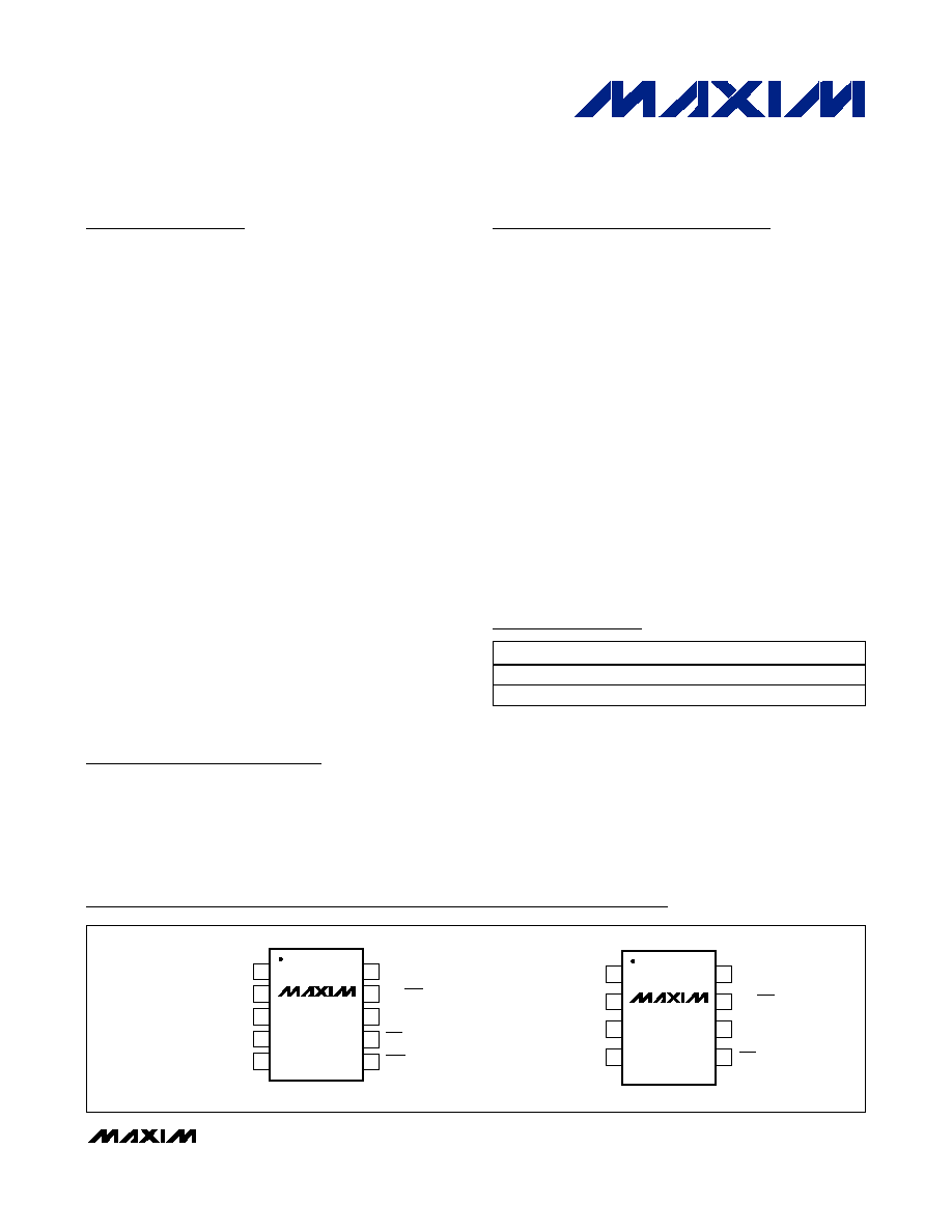
WDI
PFO
GND
1
2
8
7
CLOCK
RST/RST
WDS1
WDS2
V
CC
TOP VIEW
3
4
6
5
MAX7388
µMAX
Pin Configurations
Ordering Information
PART
TEMP RANGE
PIN-PACKAGE
PKG CODE
MAX7387srff -40
o
C to +125
o
C 10 µMAX
U10-2
MAX7388srff -40
o
C to +125
o
C 8 µMAX
U8-1
Note: "s" is a placeholder for the reset output type. Insert the
symbol found in Table 3 in the place of "s." "r" is a placeholder
for the power-on reset (POR) voltage. Insert the symbol found in
Table 2 in the place of "r." "ff" is a placeholder for the nominal
output frequency. Insert the symbol found in Table 4 in the
place of "ff." For example, MAX7387CMTP describes a device
with 4.38V reset level, open-collector RST output, and a clock
output frequency of 8MHz.
Typical Application Circuit, Functional Diagram, and Selector
Guide appear at end of data sheet.
µMAX is a registered trademark of Maxim Integrated Products, Inc.
1
2
3
4
5
10
9
8
7
6
CLOCK
RST/RST
WDI
PFO
WDS2
WDS1
V
CC
PFI
MAX7387
TOP VIEW
µMAX
WDO
GND
MAX7387/MAX7388
System Monitoring Oscillator with
Watchdog and Power Fail
2
_______________________________________________________________________________________
ABSOLUTE MAXIMUM RATINGS
Stresses beyond those listed under "Absolute Maximum Ratings" may cause permanent damage to the device. These are stress ratings only, and functional
operation of the device at these or any other conditions beyond those indicated in the operational sections of the specifications is not implied. Exposure to
absolute maximum rating conditions for extended periods may affect device reliability.
V
CC
to GND ...........................................................-0.3V to +6.0V
All Other Pins to GND ................................-0.3V to (V
CC
+ 0.3V)
CLOCK, PFO Output Current, RST/RST, WDO.................±50mA
Continuous Power Dissipation (T
A
= +70∞C)
10-Pin µMAX (derate 5.6mW/∞C over +70∞C) ..............444mW
8-Pin µMAX (derate 4.5mW/∞C over +70∞C) ................362mW
Operating Temperature Range .........................-40∞C to +125∞C
Junction Temperature ......................................................+150∞C
Storage Temperature Range .............................-65∞C to +150∞C
Lead Temperature (soldering, 10s) .................................+300∞C
ELECTRICAL CHARACTERISTICS
(Typical Application Circuit, V
CC
= +2.7V to +5.5V, T
A
= -40∞C to +125∞C, 1MHz to 16MHz output frequency range, typical values at
V
CC
= +5.0V, T
A
= +25∞C, unless otherwise noted.) (Note 1)
PARAMETER
SYMBOL
CONDITIONS
MIN
TYP
MAX
UNITS
POWER REQUIREMENTS
Operating Supply Voltage
V
CC
2.7
5.5
V
T
A
= 0
∞C to +85∞C
1.1
Valid RST/RST Supply Voltage
V
CCR
T
A
= -40
∞C to +125∞C
1.18
V
f
CLOCK
= 12MHz
5.5
Operating Supply Current
I
CC
f
CLOCK
= 8MHz
4.5
mA
TRI-LEVEL ANALOG INPUTS: WDS1, WDS2
Input-High Voltage Level
V
C C
- 0.55V
V
Input-Middle Voltage Level
0.9
V
CC
- 1.1V
V
Input-Low Voltage Level
0.45
V
LOGIC INPUT: WDI
Input Leakage Current
I
LEAK
Input high
0.5
µA
Logic-Input High Voltage
V
IH
0.7 x V
CC
V
Logic-Input Low Voltage
V
IL
0.3 x V
CC
V
PUSH-PULL LOGIC OUTPUTS: RST/
RST
Output High
V
OH
I
SOURCE
= 1mA
V
CC
- 1.5
V
Output Low
V
OL
I
SINK
= 3mA
0.05
0.4
V
OPEN-DRAIN LOGIC OUTPUTS:
RST, PFO, WDO
Output Low
V
OLO
I
SINK
= 3mA
0.05
0.4
V
OUTPUT: CLOCK
Output High Voltage
V
OHC
I
SOURCE
= 5mA
V
CC
- 0.3
V
Output Low Voltage
V
OLC
I
SINK
= 5mA
0.3
V
T
A
= 0
∞C to +85∞C, V
CC
= 5.0V
-2.75
+2.75
CLOCK Accuracy
f
CLOCK
T
A
= -40
∞C to +125∞C, V
CC
= 5.0V
-4
+4
%
Clock Frequency Temperature
Coefficient
V
CC
= 5.0V (Note 2)
140
400
ppm/∞C
Clock Frequency Supply
Voltage Coefficient
T
A
= +25∞C (Note 2)
0.67
1
%/V
CLOCK Duty Cycle
(Note 2)
45
50
55
%
MAX7387/MAX7388
System Monitoring Oscillator with
Watchdog and Power Fail
_______________________________________________________________________________________
3
ELECTRICAL CHARACTERISTICS (continued)
(Typical Application Circuit, V
CC
= +2.7V to +5.5V, T
A
= -40∞C to +125∞C, 1MHz to 16MHz output frequency range, typical values at
V
CC
= +5.0V, T
A
= +25∞C, unless otherwise noted.) (Note 1)
PARAMETER
SYMBOL
CONDITIONS
MIN
TYP
MAX
UNITS
CLOCK Output Jitter
Observation for 20s using a 500MHz
oscilloscope
310
ps
RMS
Output Rise Time
t
R
C
L OA D
= 10p F, 10% to 90% of ful l scal e ( N ote 2)
2.5
7.0
ns
Output Fall Time
t
F
C
L OA D
= 10p F, 90% to 10% of ful l scal e ( N ote 2)
2.8
7.5
ns
INTERNAL POWER-ON RESET
T
A
= +25∞C
V
TH
- 1.5%
V
TH
+ 1.5%
V
TH+
V
CC
rising, Table 2
T
A
= -40∞C to +125∞C
V
TH
- 2.5%
V
TH
+ 2.5%
Reset Voltage
V
TH-
V
CC
falling
0.98 x
V
TH+
V
Reset Timeout Period
t
RST
Figures 1, 2
86
135
250
µs
WATCHDOG
WDS1 = GND, WDS2 = GND
11
16
22
WDS1 = open, WDS2 = GND
22
32
44
WDS1 = V
CC
, WDS2 = GND
44
64
88
WDS1 = GND, WDS2 = open
88
128
177
WDS1 = open, WDS2 = open
177
256
354
WDS1 = V
CC
, WDS2 = open
354
512
708
WDS1 = GND, WDS2 = V
CC
708
1024
1416
WDS1 = open, WDS2 = V
CC
1416
2048
2832
ms
Watchdog Timeout Period
(Figure 2)
t
WDG
W D S 1 = W D S 2 = V
C C
( w atchd og d i sab l ed )
POWER FAIL
Power-Fail Select Threshold
V
SEL
PFI input
0.65 x
V
CC
0.85 x
V
CC
V
V
CC
Monitoring Threshold
(Internal Threshold)
V
ITH
V
CC
rising
4.06
4.38
4.60
V
Internal Threshold Hysteresis
V
IHYST
V
CC
falling
1.0
2
4.0
%V
ITH
PFI Monitoring Threshold
(External Threshold)
V
ETH
PFI rising
0.9
1.1
1.4
V
External Threshold Hysteresis
V
EHYST
PFI falling
1.0
3.5
8.0
%V
ETH
Note 1: All parameters are tested at T
A
= +25∞C. Specifications over temperature are guaranteed by design.
Note 2: Guaranteed by design. Not production tested.

MAX7387/MAX7388
System Monitoring Oscillator with
Watchdog and Power Fail
4
_______________________________________________________________________________________
FREQUENCY vs. SUPPLY VOLTAGE
MAX7387/88 toc01
V
CC
(V)
NORMALIZED FREQUENCY
4.85
4.20
3.55
0.990
1.000
1.010
1.020
0.980
2.90
5.50
NORMALIZED TO V
CC
= +5V
V
TH+
= +2.9V
FREQUENCY vs. TEMPERATURE
MAX7387/88 toc02
TEMPERATURE (
∞C)
NORMALIZED FREQUENCY
110
95
80
65
50
35
20
5
-10
-25
0.990
1.000
1.010
1.020
1.030
1.040
0.980
-40
125
NORMALIZED TO T
A
= +25
∞C
DUTY CYCLE vs. SUPPLY VOLTAGE
MAX7387/88 toc03
V
CC
(V)
DUTY CYCLE (%)
4.85
4.20
3.55
49
50
51
52
48
2.90
5.50
V
TH+
= +2.9V
Typical Operating Characteristics
(Typical Application Circuit, V
CC
= +5V, T
A
= +25∞C, unless otherwise noted.)
DUTY CYCLE vs. TEMPERATURE
MAX7387/88 toc04
DUTY CYCLE (%)
49
50
51
52
48
TEMPERATURE (
∞C)
110
95
80
65
50
35
20
5
-10
-25
-40
125
CLOCK OUTPUT WAVEFORM
WITH C
L
= 10pF
MAX7387/88 toc05
40ns/div
CLOCK
1V/div
V
CC
= +3.3V
CLOCK OUTPUT WAVEFORM
WITH C
L
= 50pF
MAX7387/88 toc06
40ns/div
CLOCK
1V/div
V
CC
= +3.3V
CLOCK OUTPUT WAVEFORM
WITH C
L
= 100pF
MAX7387/88 toc07
40ns/div
CLOCK
1V/div
SUPPLY CURRENT vs. TEMPERATURE
MAX7387/88 toc08
I
CC
(mA)
2
3
4
5
1
TEMPERATURE (
∞C)
110
95
80
65
50
35
20
5
-10
-25
-40
125
V
CC
= 5V
V
CC
= 3.3V
SUPPLY CURRENT vs. SUPPLY VOLTAGE
MAX7387/88 toc09
V
CC
(V)
I
CC
(mA)
4.85
4.20
3.55
2
3
4
5
1
2.90
5.50
V
TH+
= 2.9V

MAX7387/MAX7388
System Monitoring Oscillator with
Watchdog and Power Fail
_______________________________________________________________________________________
5
CLOCK SETTLING TIME FROM START
MAX7387/88 toc10
1
µs/div
CLOCK
2V/div
V
CC
2V/div
POWER-ON RESET BEHAVIOR
MAX7387/88 toc11
100
µs/div
CLOCK
5V/div
V
CC
2V/div
RST
5V/div
PFO
5V/div
t
RST
PFI = V
CC
MAXIMUM V
CC
TRANSIENT DURATION
vs. RESET THRESHOLD OVERDRIVE
MAX7387/88 toc12
RESET THRESHOLD OVERDRIVE (mV)
TRANSIENT DURATION (
µ
s)
900
800
700
600
500
400
300
200
10
100
1000
1
100
1000
RESET OCCURS ABOVE THIS CURVE
V
CC
FALLING FROM V
TH+
+ 100mV
Typical Operating Characteristics (continued)
(Typical Application Circuit, V
CC
= +5V, T
A
= +25∞C, unless otherwise noted.)
RESPONSE OF RST AND WDO
WDI EXCEEDING t
WDG
MAX7387/88 toc13
2ms/div
WDO
5V/div
WDI
2V/div
RST
5V/div
t
RST
t
WDG
RISING THRESHOLD vs. TEMPERATURE
MAX7387/88 toc14
TEMPERATURE (
∞C)
V
TH+
(V)
110
95
80
65
50
35
20
5
-10
-25
2.82
2.84
2.86
2.88
2.90
2.80
-40
125