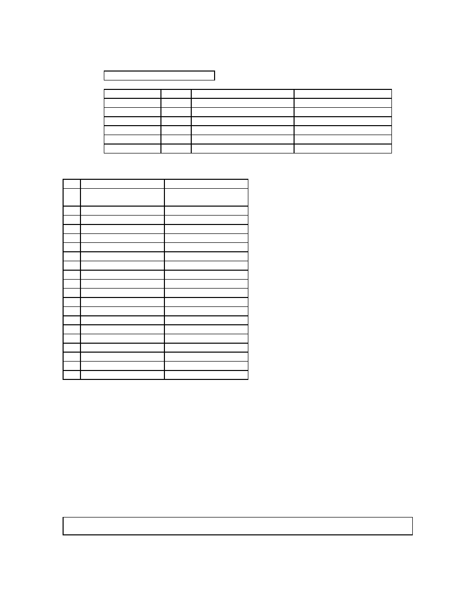
SCOPE: +5V, +12V, +15V STEP-UP, CURRENT-MODE PWM DC-DC CONVERTER
Device Type Generic Number Circuit Function
01
MAX731(x)/883B +5V
02 MAX732(x)/883B +12V
03 MAX733(x)/883B +15V
Case Outline(s). The case outlines shall be designated in Mil-Std-1835 and as follows:
Outline Letter Mil-Std-1835 Case Outline Package Code
Maxim SMD
JA
P GDIP1-T8 or CDIP2-T8 8 LEAD CERDIP J8
LP 2 CQCC1-N20 20 LEADLESS CHIP L20
Absolute Maximum Ratings
V+, LX to GND ................................................................................................... +17V, -0.3V
V
OUT
...................................................................................................................
Ī
25V
_____
Input Voltage, SS, CC, SHDN ............................................................... -0.3V to (V+ +0.3V)
Peak Switch Current (I
LX
) .............................................................................................. 1.5A
Reference Current (I
VREF
) ........................................................................................... 2.5mA
Lead Temperature (soldering, 10 seconds) ....................................................................... +300
į
C
Storage Temperature .......................................................................................... -65
į
C to +150
į
C
Continuous Power Dissipation .................................................................................. T
A
=
+
70
į
C
8 pin CERDIP(derate 8.0mW/
į
C above +70
į
C) ............................................................ 640mW
20 pin LCC(derate 9.1mW/
į
C above +70
į
C) ................................................................ 727mW
Junction Temperature T
J
.............................................................................................. +150
į
C
Thermal Resistance, Junction to Case,
JC
8 pin CERDIP........................................................................................................... 55
į
C/W
20 pin LCC ............................................................................................................. 20
į
C/W
Thermal Resistance, Junction to Ambient,
JA:
8 pin CERDIP......................................................................................................... 125
į
C/W
20 pin LCC ........................................................................................................... 110
į
C/W
Recommended Operating Conditions
Ambient Operating Range (T
A
) .................................................................... -55
į
C to
+
125
į
C
PART
INPUT SUPPY RANGE
OUTPUT VOLTAGE
GUARANTEED OUTPUT
CURRENT (mA)
MAX731
2.7V to 4.65V
+5V
200
MAX732
4.5V to 9.3V
+12V
150
MAX732
6.0V to 9.3V
+12V
200
MAX733
4.5V to 11.0V
+15V
100
MAX733
6.0V to 11.0V
+15V
200
Stresses beyond those listed under "Absolute Maximum Ratings" may cause permanent damage to the
device. These are stress ratings only, and functional operation of the device at these or any other conditions
beyond those indicated in the operational sections of the specifications is not implied. Exposure to absolute
maximum rating conditions for extended periods may affect device reliability.
----------------------------
Electrical Characteristics of MAX731/732/733/883B
19-0076
Rev. D
For /883B and SMD 5962-94621
Page 2 of
6

TABLE 1. ELECTRICAL TESTS:
TEST
Symbol
CONDITIONS
-55
į
C
T
A
+125
į
C 1/
V
IN
=+3V for 01, V+=5V for
02, 03, GND=0V, I
LOAD
=0mA
Unless otherwise specified
Group A
Subgroup
Device
type
Limits
Min
Limits
Max
Units
Output Voltage NOTE 1
V
OUT
V
IN
=2.7V to 4.65V, 2/
0mA<I
LOAD
<200mA
V+=4.5V to 9.3V,
0mA<I
LOAD
<150mA
V+=6.0V to 9.3V,
0mA<I
LOAD
<200mA
V+=4.5V to 11V,
0mA<I
LOAD
<100mA
V+=6.0V to 11V,
0mA<I
LOAD
<125mA
1,2,3
1,2,3
1,2,3
01
02
03
4.75
11.40
11.40
14.25
14.25
5.25
12.60
12.60
15.75
15.75
V
Input Voltage Range
V
IR
1,2,3
01
02
03
2.7
4.0
4.0
4.65
9.3
11.0
V
Supply Current
I
S
Includes switch current
1,2,3
01
02,03
4.0
3.0
mA
Standby Current
I
STDBY
_____
SHDN = 0V, entire circuit
1,2,3
All
100.0
Ķ
A
Shutdown input threshold
V
IH
V
IL
1,2,3
All
2.0
0.25
V
Shutdown input leakage
current
I
SIL
1,2,3
All
1.0
Ķ
A
Undervoltage Lockout
V
UL
1,2,3
02,03
4.0 V
Reference Voltage
V
REF
1,2,3
All
1.15
1.30 V
Oscillator frequency
f
O
1,2,3
01
02,03
125
130
215
210
kHz
Minimum Start-up Input
Voltage
I
LOAD
=200mA
1,2,3
01
2.5 V
Output Current
1,2,3
01
200
mA
NOTE 1: Capacitors used in automatic test setup may be different from value suggested.
Capacitor suggested values are:
V+ to GND: 150
Ķ
F & 0.1
Ķ
F (01,02,03). Output to GND: 300
Ķ
F (02,03), 150
Ķ
F (01).
V
OUT
to CC: 0.15
Ķ
F (01,02,03). CC to GND: 2200
Ķ
F (02,03), 0.15
Ķ
F (01).
VREF to GND: 0.01
Ķ
F (02,03), 4.7
Ķ
F (01). SS to GND: 0.1
Ķ
F (02,03), 0.15
Ķ
F (01).
NOTE 2: Circuit will regulate properly with input voltage as high as 5.25V due to voltage drop across the
external diode.
----------------------------
Electrical Characteristics of MAX731/732/733/883B
19-0076
Rev. D
For /883B and SMD 5962-94621
Page 3 of
6
QUALITY ASSURANCE
Sampling and inspection procedures shall be in accordance with MIL-Prf-38535, Appendix A as specified
in Mil-Std-883.
Screening shall be in accordance with Method 5004 of Mil-Std-883. Burn-in test Method 1015:
1. Test Condition, A, B, C, or D.
2. TA = +125
į
C minimum.
3. Interim and final electrical test requirements shall be specified in Table 2.
Quality conformance inspection shall be in accordance with Method 5005 of Mil-Std-883, including
Groups A, B, C, and D inspection.
Group A inspection:
1. Tests as specified in Table 2.
2. Selected subgroups in Table 1, Method 5005 of Mil-Std-883 shall be omitted.
Group C and D inspections:
a. End-point electrical parameters shall be specified in Table 1.
b. Steady-state life test, Method 1005 of Mil-Std-883:
1. Test condition A, B, C, D.
2. TA = +125
į
C, minimum.
3. Test duration, 1000 hours, except as permitted by Method 1005 of Mil-Std-883.
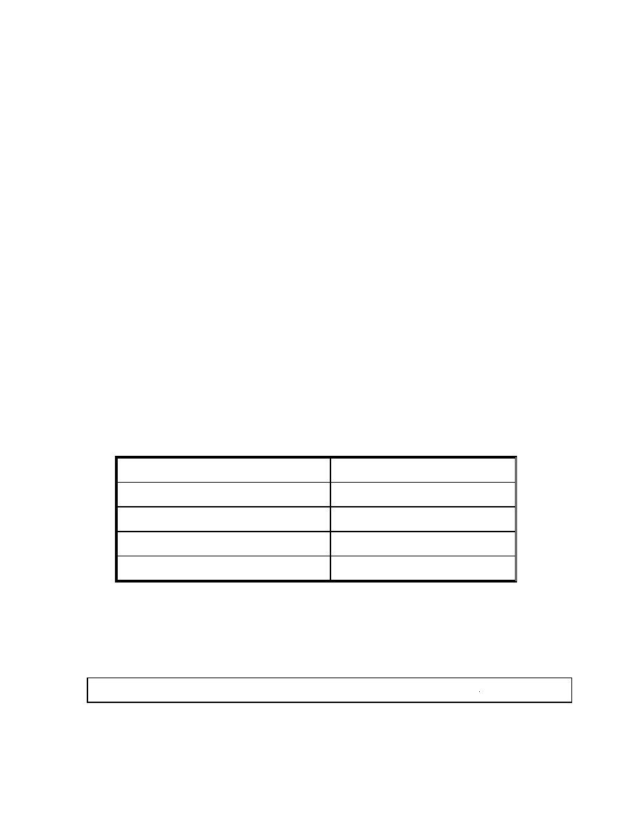
TABLE 2. ELECTRICAL TEST REQUIREMENTS
Mil-Std-883 Test Requirements
Subgroups
per Method 5005, Table 1
Interim Electric Parameters
Method 5004
1
Final Electrical Parameters
Method 5005
1*, 2, 3
Group A Test Requirements
Method 5005
1, 2, 3
Group C and D End-Point Electrical Parameters
Method 5005
1
* PDA applies to Subgroup 1 only.
----------------------------
Electrical Characteristics of MAX731/732/733/883B
19-0076
Rev. D
For /883B and SMD 5962-94621
Page 5 of
6