 | –≠–ª–µ–∫—Ç—Ä–æ–Ω–Ω—ã–π –∫–æ–º–ø–æ–Ω–µ–Ω—Ç: MAX7428 | –°–∫–∞—á–∞—Ç—å:  PDF PDF  ZIP ZIP |

General Description
The MAX7428/MAX7430/MAX7432 filters are low-cost,
high-performance replacements for standard discrete fil-
ter and buffer solutions. The MAX7428/MAX7430/
MAX7432 are ideal for anti-aliasing and DAC smoothing
video applications, when analog video is reconstructed
from a digital data stream. These devices require a sin-
gle +5V supply and the filters have a cutoff frequency
optimized for NTSC, PAL, and standard definition digital
TV (SDTV) video signals. The MAX7428/MAX7430/
MAX7432 feature Maxim's Single Pin Bus (MSPBTM)
interface to digitally control channel selection (IN_A or
IN_B), adjust high-frequency boost, bypass the filter,
configure luma vs. chroma operation, and control the
output disable. The MAX7428 single-channel filter is
ideal for composite (CVBS) video signals. The MAX7430
dual filter is optimized for S-Video (Y/C) applications. The
MAX7432 triple filter is optimized for component (YP
b
P
r
or embedded synchronous RGB) video signals. The
MAX7428 is available in a tiny 8-pin SOT23 package, the
MAX7430 is available in a miniature 10-pin µMAX pack-
age, and the MAX7432 is available in a 14-pin TSSOP
package. The MAX7428/MAX7430/MAX7432 are fully
specified over the -40∞C to +85∞C extended temperature
range.
Applications
Set-Top Boxes
DVD Players
Hard-Disk Recorders
Camcorders
Features
o Ideal for CVBS, Y/C (S-Video), and RGB (Y P
b
P
r
)
Outputs for NTSC, PAL, and SDTV
o 6th-Order Lowpass Filter
o Drives Two 150 Video Loads
o Four Levels of Passband High-Frequency
Boost Control
o Input 2 to 1 Multiplexer
o Output Disable
o Filter Bypassing
o +5V Single-Supply Voltage
o Tiny 8-Pin SOT23 Package (MAX7428), 10-Pin
µMAX Package (MAX7430), and 14-Pin TSSOP
Package (MAX7432)
MAX7428/MAX7430/MAX7432
Standard Definition Video Reconstruction
Filters and Buffers
________________________________________________________________ Maxim Integrated Products
1
+6dB
LEVEL SHIFT
6TH-ORDER
FILTER
OUT
SERIAL INTERFACE
AND CONTROL
DATA
D/A
INA
INB
*
*OPTIONAL
SYNC
AUX INPUT
BIAS GENERATOR
GND
REXT
ENCODER
MAX7428
SYNCIO
V
CC
75
75
C
IN
C
IN
*
Functional Diagrams
Ordering Information
19-2119; Rev 2; 9/02
Pin Configurations appear at end of data sheet.
Functional Diagrams continued at end of data sheet.
For pricing, delivery, and ordering information, please contact Maxim/Dallas Direct! at
1-888-629-4642, or visit Maxim's website at www.maxim-ic.com.
PART
TEMP
RANGE
PIN-
PACKAGE
TOP
MARK
MAX7428EKA-T
-40
∞C to +85∞C
8 SOT23-8
AAIU
MAX7430EUB
-40
∞C to +85∞C
10 µMAX
--
MAX7432EUD
-40
∞C to +85∞C
14 TSSOP
--
MSPB is a trademark of Maxim Integrated Products, Inc.
MAX7428/MAX7430/MAX7432
Standard Definition Video Reconstruction
Filters and Buffers
2
_______________________________________________________________________________________
ABSOLUTE MAXIMUM RATINGS
ELECTRICAL CHARACTERISTICS
(V
CC
= +5V ±10%, R
REXT
= 300k
±1%, C
IN
= 0.1µF, C
REXT
= (1nF to 1µF) ±1%, C
LOAD
= 0 to 20pF; BOOST0_, BOOST1_ = 0, 0;
T
A
= T
MIN
to T
MAX
, unless otherwise noted. Typical values are at T
A
= +25∞C.) (Note 2)
Stresses beyond those listed under "Absolute Maximum Ratings" may cause permanent damage to the device. These are stress ratings only, and functional
operation of the device at these or any other conditions beyond those indicated in the operational sections of the specifications is not implied. Exposure to
absolute maximum rating conditions for extended periods may affect device reliability.
V
CC
to GND ...........................................................................+6V
All Other Pins to GND .................................-0.3V to (V
CC
+ 0.3V)
Maximum Current Into Any Pin .........................................
±
50mA
Continuous Power Dissipation (T
A
= +70∞C)
8-Pin SOT23 (derate 9.71mW/∞C above +70∞C)..........777mW
10-Pin µMAX (derate 6.94mW/∞C above +70∞C) ......555.5mW
14-Pin TSSOP (derate 9.1mW/∞C above +70∞C) .........727mW
Operating Temperature Range ...........................-40∞C to +85∞C
Storage Temperature Range .............................-65∞C to +150∞C
Junction Temperature ......................................................+150∞C
Lead Temperature (soldering, 10s) .................................+300∞C
PARAMETER
SYMBOL
CONDITIONS
MIN
TYP
MAX
UNITS
f = 100kHz to 4.2MHz relative to 100kHz
-0.5
+0.5
Passband Response
f = 100kHz to 5MHz relative to 100kHz
-1.0
+1.0
dB
Stopband Attenuation
A
sb
f
>
27MHz
48
dB
HF Boost Relative Step Size, 4
Levels
f = 4.2MHz to 5MHz
0.2
0.4
0.6
dB
Differential Gain
dG
5-step modulated staircase
0.2
%
Differential Phase
d
5-step modulated staircase
0.2
degrees
Harmonic Distortion
THD
f = 100kHz to 5MHz
0.1
0.5
%
Signal-to-Noise Ratio
SNR
Peak signal (2Vp-p) to RMS noise,
f = 100Hz to 50MHz
72
dB
Group Delay Deviation
t
g
Deviation from 100kHz to 3.58 (4.43)MHz
20
ns
Line-Time Distortion
H
dist
18µs, 100 IRE bar
0.3
%
Field-Time Distortion
V
dist
130 lines, 18µs, 100 IRE bar
0.5
%
Clamp Settling Time
t
clamp
to ±1% (Note 1)
100
Lines
CLEVEL = 0
0.8
1.3
Output DC Clamp Level
CLEVEL = 1
1.35
1.85
V
Low-Frequency Gain
A
V
Gain at 100kHz
1.9
1.975
2.05
V/V
Group Delay Matching
t
g(MATCH)
Low frequency channel-to-channel matching
f = 100kHz
2
ns
Low-Frequency Gain Matching
A
V(MATCH)
C hannel - to- channel g ai n m atchi ng , f = 100kH z
5
%
Channel-to-Channel Crosstalk
X
TALK
Channel-to-channel crosstalk, f = 100kHz
to 5.5MHz
-60
dB
Output Short-Circuit Current
I
SC
OUT_ shorted to ground or V
CC
50
mA
Input Leakage Current
I
IN
10
µA
Y
INp-p
CLEVEL = 0
1.4
Input Dynamic Swing
C
INp-p
CLEVEL = 1
0.9
Vp-p
V
CC
Supply Range
V
CC
4.5
5.5
V

MAX7428/MAX7430/MAX7432
Standard Definition Video Reconstruction
Filters and Buffers
_______________________________________________________________________________________
3
ELECTRICAL CHARACTERISTICS (continued)
(V
CC
= +5V ±10%, R
REXT
= 300k
±1%, C
IN
= 0.1µF, C
REXT
= (1nF to 1µF) ±1%, C
LOAD
= 0 to 20pF; BOOST0_, BOOST1_ = 0, 0;
T
A
= T
MIN
to T
MAX
, unless otherwise noted. Typical values are at T
A
= +25∞C.) (Note 2)
MSPB INTERFACE TIMING SPECIFICATIONS
(V
CC
= +5V ±10%, R
REXT
= 300k
±1%, C
REXT
= (1nF to 1µF) ±1%, C
LOAD
= 0 to 20pF, T
A
= T
MIN
to T
MAX
, unless otherwise noted.
Typical values are at T
A
= +25∞C.) (Figures 4 through 9)
Note 1: One horizontal line = 63.5µs.
Note 2: MAX7428 devices are 100% production tested at T
A
= +25∞C and are guaranteed by design from T
A
= T
MIN
to T
MAX
.
PARAMETER
SYMBOL
CONDITIONS
MIN
TYP
MAX
UNITS
MSPB TIMING
Logic-Zero/Prompt Pulse Width
t
0
, t
P
1
5
8
µs
Logic-One Pulse Width
t
1
24
30
36
µs
Transaction Pulse Width
t
T
80
100
120
µs
Separation Between Pulses
t
WAIT
0.5
µs
Bus Release Time by Host After
Prompt Pulse
t
RELEASE
1
µs
Bus Reclaim Time by Host After
Prompt Pulse
t
RECLAIM
13
µs
Read Back Data Valid Window
After the Prompt Pulse
t
READ
2.3
4.7
µs
PARAMETER
SYMBOL
CONDITIONS
MIN
TYP
MAX
UNITS
MAX7428
24
32
MAX7430
45
62
Supply Current
I
CC
No load
MAX7432
68
86
mA
Power-Supply Rejection Ratio
PSRR
V
IN
= 100mVp-p, f = 0 to 5.5MHz
40
dB
IN_A/IN_B Crosstalk
V
IN
= 100mVp-p, f = 100kHz to 5.5MHz
-60
dB
LOGIC CHARACTERISTICS
Logic Input High Voltage
V
IH
2
V
Logic Input Low Voltage
V
IL
0.8
V
Logic Input Current
I
IH
/I
IL
V
IL
= 0 (source), V
IH
= V
CC
(sink)
10
µA
Logic Output High Voltage
V
OH
I
(SOURCE)
= 500µA
V
CC
-
0.5
V
Logic Output Low Voltage
V
OL
I
(SINK)
= 500µA
0.4
V

MAX7428/MAX7430/MAX7432
Standard Definition Video Reconstruction
Filters and Buffers
4
_______________________________________________________________________________________
Typical Operating Characteristics
(V
CC
= +5V, R
REXT
= 300k
; BOOST0_, BOOST1_ = 0, 0; V
IN_
= 1Vp-p, T
A
= +25∞C, unless otherwise noted.)
0.1
1
10
100
AMPLITUDE vs. FREQUENCY
MAX7428/30/32 toc01
FREQUENCY (MHz)
AMPLITUDE (dB)
0
-60
-50
-40
-30
-20
-10
0.1
1
10
PASSBAND AMPLITUDE vs. FREQUENCY
MAX7428/30/32 toc02
FREQUENCY (MHz)
AMPLITUDE (dB)
2
-10
-8
-6
-4
-2
0
A
C
D
B
A: BOOST1, BOOST0 = 1, 1
B: BOOST1, BOOST0 = 1, 0
C: BOOST1, BOOST0 = 0, 1
D: BOOST1, BOOST0 = 0, 0
0.1
1
10
PHASE RESPONSE vs. FREQUENCY
MAX7428/30/32 toc03
FREQUENCY (MHz)
PHASE (DEGREES)
180
-180
-120
-60
0
60
120
0.1
1
10
GROUP DELAY vs. FREQUENCY
MAX7428/30/32 toc04
FREQUENCY (MHz)
GROUP DELAY (ns)
120
0
20
40
60
80
100
200ns/div
2T RESPONSE (1IRE = 7.14mV)
INA_
200mV/div
OUT_
200mV/div
MAX7428/30/32 toc05
400ns/div
MODULATED 12.5T RESPONSE
(1IRE = 7.14mV)
INA_
200mV/div
OUT_
200mV/div
MAX7428/30/32 toc06
22
24
23
26
25
27
28
-40
10
-15
35
60
85
SUPPLY CURRENT vs. TEMPERATURE
MAX7428/30/32 toc07
TEMPERATURE (
∞C)
SUPPLY CURRENT (mA)
NO LOAD
0.2
0.1
0
-0.1
-0.2
-0.3
DIFFERENTIAL GAIN (%)
0
-0.01
-0.04
-0.08
-0.10
-0.06
1st.
2nd.
3rd.
4th.
5th.
6th.
DIFFERENTIAL GAIN
MAX7428/30/32 toc08
MAX7428/30/32 toc09
0.20
0.15
0.10
0.05
0
-0.05
1st.
2nd.
3rd.
4th.
5th.
6th.
0
0.04
0.06
0.06
0.04
0.02
DIFFERENTIAL PHASE (DEGREES)
DIFFERENTIAL PHASE

MAX7428/MAX7430/MAX7432
Standard Definition Video Reconstruction
Filters and Buffers
_______________________________________________________________________________________
5
0.1
1
10
OUTPUT IMPEDANCE vs. FREQUENCY
MAX7428/30/32 toc10
FREQUENCY (MHz)
IMPEDANCE
(
)
0
0.5
1.0
1.5
2.0
2.5
3.0
3.5
4.0
200ns/div
OUTPUT TRANSIENT DUE TO
INPUT MUX SWITCHING
OUT_
500mV/div
MAX7428/30/32 toc11
-70
-95
0.1
1
10
PASSBAND CHANNEL-TO-CHANNEL
CROSSTALK vs. FREQUENCY
-90
MAX7428/30/32 toc12
FREQUENCY (MHz)
CROSSTALK (dB)
-85
-80
-75
BOOST = CODE 00
Typical Operating Characteristics (continued)
(V
CC
= +5V, R
REXT
= 300k
; BOOST0_, BOOST1_ = 0, 0; V
IN
= 1Vp-p, T
A
= +25∞C, unless otherwise noted.)
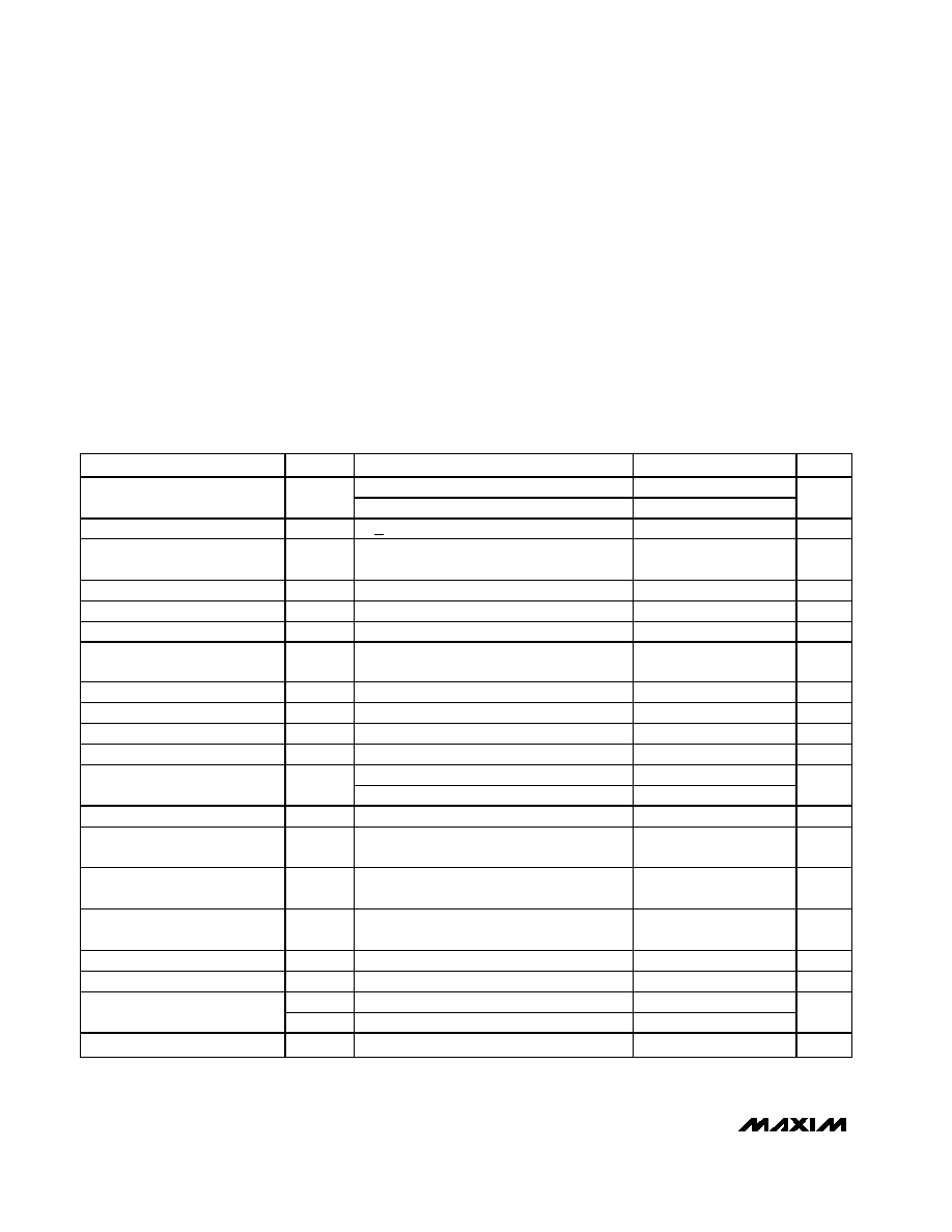
Pin Description
PIN
MAX7432
MAX7430
MAX7428
NAME
FUNCTION
1
1
--
IN1A
Video Input 1A. Master channel, sync signal required. Use a 0.1µF
series input capacitor for proper operation.
2
2
--
IN2A
Video Input 2A. Slave channel, clamping controlled by master channel
sync. Use a 0.1µF series input capacitor for proper operation.
3
--
--
IN3A
Video Input 3A. Slave channel, clamping controlled by master channel
sync. Use a 0.1µF series input capacitor for proper operation.
4, 10
8
4
GND
Ground
5
4
--
IN1B
Video Input 1B. Master channel, sync signal required. Use a 0.1µF
series input capacitor for proper operation.
6
5
--
IN2B
Video Input 2B. Slave channel, clamping controlled by master channel
sync. Use a 0.1µF series input capacitor for proper operation.
7
--
--
IN3B
Video Input 3B. Slave channel, clamping controlled by master channel
sync. Use a 0.1µF series input capacitor for proper operation.
8
6
6
DATA
Serial Data Interface
9
--
--
OUT3
Buffer Output 3
11
7
--
OUT2
Buffer Output 2
12
3
7
REXT
External Resistor. Connect a 300k
resistor from REXT to GND for
internal biasing. Connect a 1nF to 1µF capacitor from REXT to GND for
chip-address programming (see Table 3).