 | ÐлекÑÑоннÑй компоненÑ: MAX7444 | СкаÑаÑÑ:  PDF PDF  ZIP ZIP |
Äîêóìåíòàöèÿ è îïèñàíèÿ www.docs.chipfind.ru
General Description
The MAX7443/MAX7444 are low-cost, triple-channel
video reconstruction filters for S-video and CVBS video
signals. These devices are ideal for anti-aliasing and
DAC smoothing video applications such as set-top
boxes, DVD players, hard-disk recorders (HDRs), and
personal video recorders. These filters operate from a
single +5V supply. They are optimized for NTSC, PAL,
and standard-definition digital TV (SDTV) video systems.
Each channel consists of a lowpass filter and an
adjustable-gain output buffer capable of driving two
standard 150
video loads. The output buffers can drive
either an AC or a DC load such that the blanking level
voltage after the backmatch resistor is less than 1V. The
Y and C video inputs are summed to produce the com-
posite video output. The MAX7444 offers high-
frequency boost to improve picture sharpness. The
MAX7443 has a maximum flat-frequency response.
The MAX7443/MAX7444 are available in a tiny 8-pin thin
QFN and an 8-pin SO package with exposed pad, and
are fully specified over the -40°C to +85°C extended
temperature range.
Applications
Features
o Triple-Channel Filter and Buffer for CVBS and
Y/C (S-Video)
o Filter Response Ideal for NTSC, PAL, and
Interlaced SDTV Signals
o 41dB (typ) Stopband Attenuation at 27MHz
o -0.3dB (typ) Passband Response
o Low Blanking Level Voltage Allows DC-Coupled
Output
o Each Channel Drives Two 150 Video Loads
o +5V Single-Supply Voltage
o Tiny 8-Pin Thin QFN or 8-Pin SO Packages
MAX7443/MAX7444
Triple-Channel Video Reconstruction Filter and
Buffer for Composite and Y/C Outputs
________________________________________________________________ Maxim Integrated Products
1
Ordering Information
19-2749; Rev 0; 1/03
For pricing, delivery, and ordering information, please contact Maxim/Dallas Direct! at
1-888-629-4642, or visit Maxim's website at www.maxim-ic.com.
PART
TEMP RANGE
PIN-PACKAGE
TOP
MARK
MAX7443ETA
-40°C to +85°C
8 Thin QFN-EP*
AFX
MAX7443ESA
-40°C to +85°C
8 SO-EP*
--
MAX7444ETA
-40°C to +85°C
8 Thin QFN-EP*
AFY
MAX7444ESA
-40°C to +85°C
8 SO-EP*
--
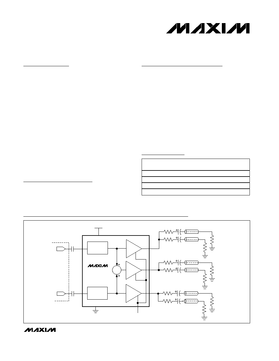
D/A
CIN
LOWPASS
FILTER
LOWPASS
FILTER
YIN
D/A
6dB/
9.5dB/
12dB
6dB/
9.5dB/
12dB
6dB/
9.5dB/
12dB
GSET
COUT
CVOUT
YOUT
*
*
*
*
*
*
*OPTIONAL
GND
V
CC
ENCODER
MAX7443
MAX7444
Functional Diagram
Set-Top Boxes/HDR/DVD
Security Cameras/Digital
Cameras
Game Consoles
Digital VCRs
Every Composite,
S-Video Output for NTSC,
PAL, SDTV
*EP = Exposed pad.
Selector Guide appears at end of data sheet.

MAX7443/MAX7444
Triple-Channel Video Reconstruction Filter and
Buffer for Composite and Y/C Outputs
2
_______________________________________________________________________________________
ABSOLUTE MAXIMUM RATINGS
Stresses beyond those listed under "Absolute Maximum Ratings" may cause permanent damage to the device. These are stress ratings only, and functional
operation of the device at these or any other conditions beyond those indicated in the operational sections of the specifications is not implied. Exposure to
absolute maximum rating conditions for extended periods may affect device reliability.
V
CC
to GND ...........................................................................+6V
All Other Pins to GND.................................-0.3V to (V
CC
+ 0.3V)
Maximum Current into Any Pin Except V
CC
and GND .....±50mA
Continuous Power Dissipation (T
A
= +70°C)
8-Pin Thin QFN (derate 24.4mW/°C above +70°C) ...1951mW
8-Pin SO (derate 18.9mW/°C above +70°C)..............1509mW
Operating Temperature Range ...........................-40°C to +85°C
Storage Temperature Range .............................-65°C to +150°C
Junction Temperature ......................................................+150°C
Lead Temperature (soldering, 10s) .................................+300°C
ELECTRICAL CHARACTERISTICS
(V
CC
= +5V ±5%, C
L
= 0 to 20pF, R
L
= 75
to GND for DC-couple, R
L
= 75
to V
CC
/2 for AC-couple, C
YIN
= C
CIN
= 0.1µF,
T
A
= T
MIN
to T
MAX
, GSET = GND (6dB) and V
CC
(9.5dB), unless otherwise noted. Typical values are at T
A
= +25°C.)
PARAMETER
SYMBOL
CONDITIONS
MIN
TYP
MAX
UNITS
MAX7443
-0.8
-0.3
+0.1
Passband Response
f = 100kHz to 4.2MHz,
relative to 100kHz
MAX7444
-0.1
+0.6
+0.92
dB
Stopband Attenuation
A
SB
f = 27MHz
39
41
dB
Boost Amplitude
f = 4.2MHz, MAX7444
0.6
dB
Differential Gain
dG
5-step modulated
staircase
Gain = 6dB,
9.5dB, 12dB
0.15
0.4
%
Differential Phase
d
5-step modulated
staircase
Gain = 6dB,
9.5dB, 12dB
0.15
0.4
Degrees
Signal-to-Noise Ratio
SNR
Peak signal (2V
P-P
) to
RMS noise, f = 100Hz to
50MHz
Gain = 6dB,
9.5dB, 12dB
67
73
dB
MAX7443
8
20
Group Delay Deviation
t
g
Deviation from 100kHz to
4.1MHz
MAX7444
12
30
ns
Line-Time Distortion
H
DIST
18µs, 100 IRE bar
0.3
%
Field-Time Distortion
V
DIST
130 lines, 18µs, 100 IRE bar
0.5
%
Clamp Settling Time
To ±1%
100
Lines
YOUT
0.6
0.8
1.0
CVOUT
0.6
0.8
1.0
Output DC Clamp Level
COUT
1.44
1.6
1.97
V
Low-Frequency Gain Accuracy
A
V
f = 100kHz, relative to 6dB
-3.5
+2
%
Group Delay Matching
t
g(MATCH)
Low-frequency channel-to-channel matching,
f = 100kHz for YOUT and COUT
2
ns
Channel-to-Channel Crosstalk
X
TALK
f = 100kHz to 3.58MHz, gain = 6dB
61
dB
Input Leakage Current
I
IN
10
µA
MAX7443/MAX7444
Triple-Channel Video Reconstruction Filter and
Buffer for Composite and Y/C Outputs
_______________________________________________________________________________________
3
ELECTRICAL CHARACTERISTICS (continued)
(V
CC
= +5V ±5%, C
L
= 0 to 20pF, R
L
= 75
to GND for DC-couple, R
L
= 75
to V
CC
/2 for AC-couple, C
YIN
= C
CIN
= 0.1µF,
T
A
= T
MIN
to T
MAX
, GSET = GND (6dB) and V
CC
(9.5dB), unless otherwise noted. Typical values are at T
A
= +25°C.)
PARAMETER
SYMBOL
CONDITIONS
MIN
TYP
MAX
UNITS
Y
INP-P
GSET = GND (6dB)
1.2
Input Dynamic Swing
C
INP-P
GSET = GND (6dB)
0.9
V
P-P
SUPPLY
Supply Voltage Range
V
CC
4.75
5.25
V
Supply Current
I
CC
V
CC
= +5.25V, no load
88
110
mA
Power-Supply Rejection Ratio
PSRR
V
IN
= 100mV
P-P
, f = 0 to 3.5MHz
33
dB
Typical Operating Characteristics
(V
CC
= +5V, T
A
= +25°C, unless otherwise noted.)
-80
1
10
100
AMPLITUDE vs. FREQUENCY
MAX7443/44 toc01
FREQUENCY (MHz)
AMPLITUDE (dB)
-60
-20
-40
0
NORMALIZED TO 0dB
-2.0
0.1
1
10
PASSBAND AMPLITUDE vs. FREQUENCY
MAX7443/44 toc02
FREQUENCY (MHz)
AMPLITUDE (dB)
0.5
-0.5
2.0
NORMALIZED TO 0dB
1.5
1.0
-1.5
-1.0
0
MAX7443
MAX7444
-200
0.1
1
10
PHASE RESPONSE vs. FREQUENCY
MAX7443/44 toc03
FREQUENCY (MHz)
PHASE (DEGREES)
50
-50
200
150
100
-150
-100
0
40
0.1
1
10
GROUP DELAY vs. FREQUENCY
MAX7443/44 toc04
FREQUENCY (MHz)
GROUP DELAY (ns)
70
60
90
80
50
2T RESPONSE (1 IRE = 7.14mV)
MAX7443/44 toc05
200ns/div
Y
IN
200mV/div
Y
OUT
400mV/div
MODULATED 12.5T RESPONSE
(1 IRE = 7.14mV)
MAX7443/44 toc06
400ns/div
Y
IN
200mV/div
Y
OUT
200mV/div
MAX7443/MAX7444
Triple-Channel Video Reconstruction Filter and
Buffer for Composite and Y/C Outputs
4
_______________________________________________________________________________________
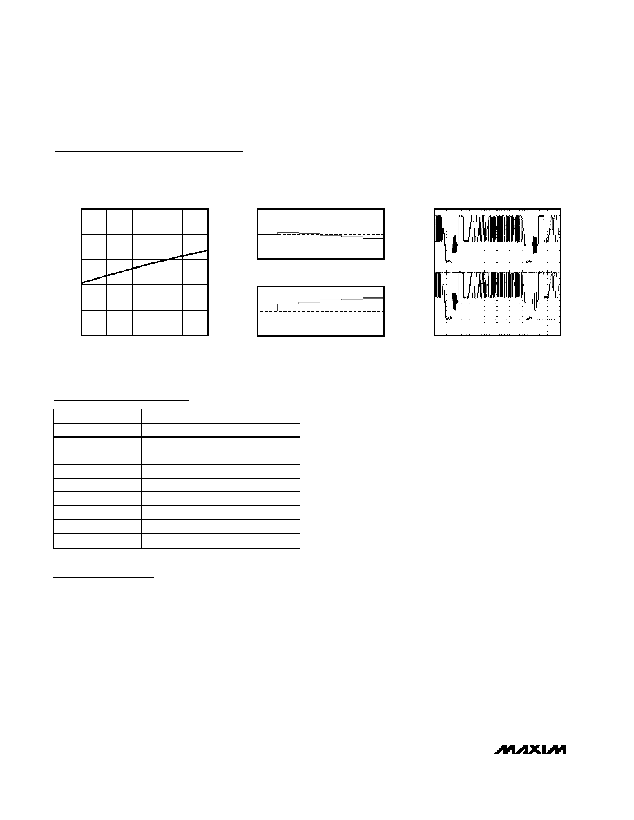
65
70
80
75
85
90
-40
10
-15
35
60
85
SUPPLY CURRENT
vs. TEMPERATURE
MAX7443/44 toc07
TEMPERATURE (
°C)
SUPPLY CURRENT (mA)
DIFFERENTIAL GAIN
MAX7443/44 toc08
DIFFERENTIAL PHASE (DEGREES)
1
3
2
4
5
6
7
1
3
2
4
5
6
7
0.2
0.3
0.1
0
-0.1
-0.2
-0.3
DIFFERENTIAL GAIN (%)
0.2
0.3
0.1
0
-0.1
-0.2
-0.3
DIFFERENTIAL PHASE
MULTIBURST RESPONSE
MAX7443/44 toc09
YIN
200mV/div
YOUT
200mV/div
10
µs/div
Typical Operating Characteristics (continued)
(V
CC
= +5V, T
A
= +25°C, unless otherwise noted.)
Detailed Description
The primary function of the MAX7443/MAX7444 is to fil-
ter and buffer the encoder DAC outputs that contain
digital video information in applications such as set-top
boxes, hard-disk recorders, DVD players, and digital
VCRs. These devices reconstruct and clean up analog
video signals. Each MAX7443/MAX7444 consists of a
lowpass filter and an adjustable-gain output video
buffer that is capable of driving two standard 150
video loads. The luma (YIN) and chroma (CIN) video
inputs are summed internally to provide the composite
(CVOUT) video output.
These devices operate from a single +5V supply. The
filters have a nominal cutoff frequency optimized for
NTSC, PAL, and SDTV.
Filter
Filter Response
The reconstruction filter consists of two 2nd-order
Sallen-Key stages. The Butterworth-type response fea-
tures a maximally flat passband for NTSC and PAL
bandwidths. The stopband offers 41dB (typ) of attenua-
tion at sampling frequencies of 27MHz and above (see
Typical Operating Characteristics).
High-Frequency Boost
The high-frequency boost available in the MAX7444
compensates for signal degradation and rolloff in the
video encoder, which increases the image sharpness.
The MAX7443 has a flat response over the video band-
width.
Output Buffer
The output buffer drives two 150
video loads with a
2V
P-P
signal. The adjustable gain of the output buffer
provides a gain of 6dB, 9.5dB, and 12dB, which are
selected by tying the GSET pin to GND, V
CC
, or float-
ing, respectively. The MAX7443/MAX7444 can drive an
AC load or drive the video load directly without using
the large output capacitor. The output buffer drives a
DC load with an output blanking level of less than 1V.
PIN
NAME
FUNCTION
1
YIN
Luma (Y) Input
2
GSET
Gain-Setting Control Input. See Table 1
for values.
3
CIN
Chroma (C) Input
4
GND
Ground
5
V
CC
5V Power Supply
6
COUT
Chroma (C) Output
7
CVOUT
Composite Video Output
8
YOUT
Luma (Y) Output
Pin Description
12dB Gain Setting
The GSET pin is biased internally to V
CC
/2 through two
100k
resistors from V
CC
to GND. The internal imped-
ance at the node is 50k
. No additional connection is
necessary since the pin offers a minimum noise margin
immunity of 1V
P-P
.
Output Clamp Level
When sync pulses in the luma signal (Y) are detected,
the DC restore loop is activated. The function of the
loop is to set the sync tip of the video signal to the
desired DC level of 0.8V for YOUT and COUT and the
average DC voltage of COUT at 1.6V.
Applications Information
Input Considerations
Use a 0.1µF ceramic capacitor to AC-couple the input
to the MAX7443/MAX7444. This input capacitor stores
a DC level such that the outputs are clamped to the
appropriate DC voltage level.
Output Considerations
The outputs of the MAX7443/MAX7444 are typically
connected to a 75
series back-match resistor fol-
lowed by the video cable. Because of the inherent
divide by two of this configuration, the blanking level of
the video cable is always less than 1V, which complies
with industry-standard video requirements. The video
buffer can also drive an AC-coupled video load. Good
video performance is achieved with an output capacitor
as low as 220µF.
Power-Supply Bypassing and Layout
The MAX7443/MAX7444 operate from a single +5V
supply. Bypass V
CC
to GND with a 0.1µF capacitor.
Place all external components as close to the device as
possible. Refer to the MAX7443 evaluation kit for a
proven PC board layout example.
Exposed Pads
Both the SO and thin QFN packages of the MAX7443/
MAX7444 have exposed pads on the bottom of the
packages. These pads are electrically connected to
GND and should be connected to the ground plane for
improved thermal conductivity. Do not route signals
under these packages.
Chip Information
TRANSISTOR COUNT: 4252
PROCESS: BiCMOS
MAX7443/MAX7444
Triple-Channel Video Reconstruction Filter and
Buffer for Composite and Y/C Outputs
_______________________________________________________________________________________________________
5
GSET
GAIN (dB)
GND
6
V
CC
9.5
Open
12
Table 1. Gain-Setting Control
COUT
V
CC
GND
1
2
8
7
YOUT
CVOUT
GSET
CIN
YIN
3
4
6
5
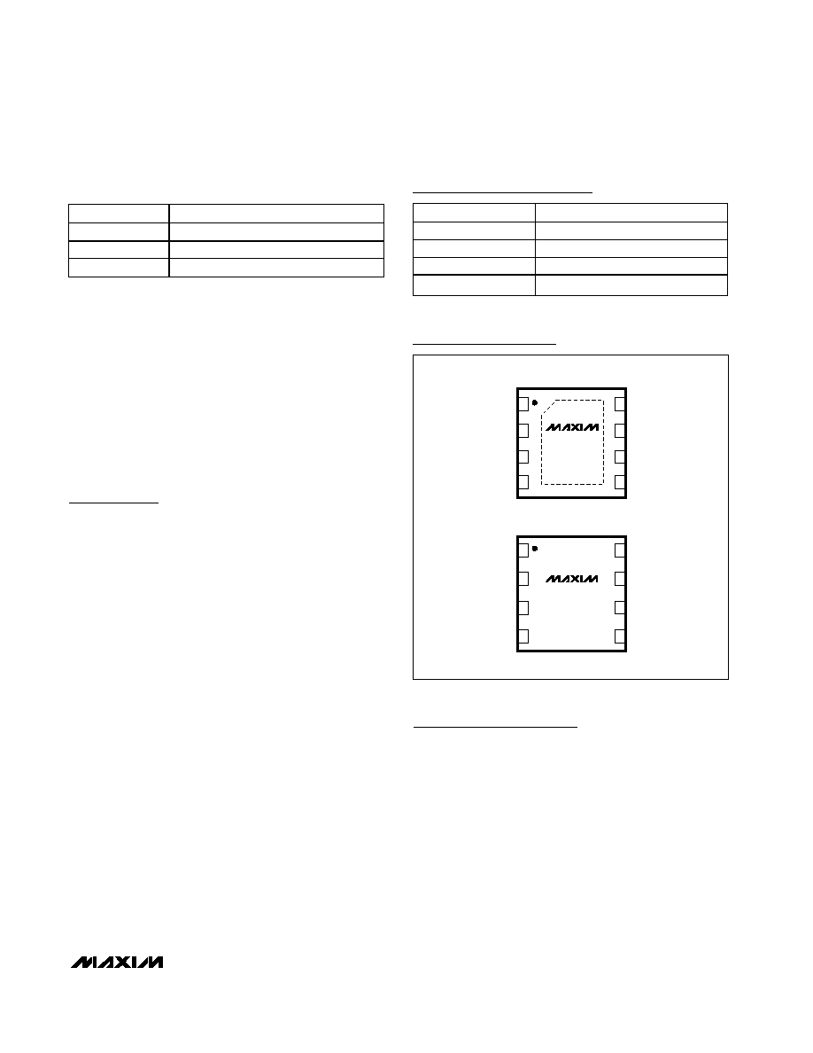
THIN QFN
TOP VIEW
COUT
V
CC
GND
1
2
8
7
YOUT
CVOUT
GSET
CIN
YIN
3
4
6
5
SO
MAX7443
MAX7444
MAX7443
MAX7444
Pin Configurations
Selector Guide
PART
HIGH-FREQUENCY BOOST
MAX7443ETA
No
MAX7443ESA
No
MAX7444ETA
Yes
MAX7444ESA
Yes