 | –≠–ª–µ–∫—Ç—Ä–æ–Ω–Ω—ã–π –∫–æ–º–ø–æ–Ω–µ–Ω—Ç: MAX745C/D | –°–∫–∞—á–∞—Ç—å:  PDF PDF  ZIP ZIP |

MAX745
Switch-Mode Lithium-Ion
Battery-Charger
________________________________________________________________ Maxim Integrated Products
1
General Description
The MAX745 provides all functions necessary for
charging lithium-ion (Li+) battery packs. It provides a
regulated charging current of up to 4A without getting
hot, and a regulated voltage with only ±0.75% total
error at the battery terminals. It uses low-cost, 1% resis-
tors to set the output voltage, and a low-cost N-channel
MOSFET as the power switch.
The MAX745 regulates the voltage set point and charg-
ing current using two loops that work together to transi-
tion smoothly between voltage and current regulation.
The per-cell battery voltage regulation limit is set
between 4V and 4.4V using standard 1% resistors, and
then the number of cells is set from 1 to 4 by pin-strap-
ping. Total output voltage error is less than ±0.75%.
For a similar device with an SMBusTM microcontroller
interface and the ability to charge NiCd and NiMH cells,
refer to the MAX1647 and MAX1648. For a low-cost Li+
charger using a linear-regulator control scheme, refer
to the MAX846A.
________________________Applications
Li+ Battery Packs
Desktop Cradle Chargers
Cellular Phones
Notebook Computers
Hand-Held Instruments
____________________________Features
o Charges 1 to 4 Li+ Battery Cells
o ±0.75% Voltage-Regulation Accuracy
Using 1% Resistors
o Provides up to 4A without Excessive Heating
o 90% Efficient
o Uses Low-Cost Set Resistors and
N-Channel Switch
o Up to 24V Input
o Up to 18V Maximum Battery Voltage
o 300kHz Pulse-Width Modulated (PWM) Operation
Low-Noise, Small Components
o Stand-Alone Operation--No Microcontroller
Needed
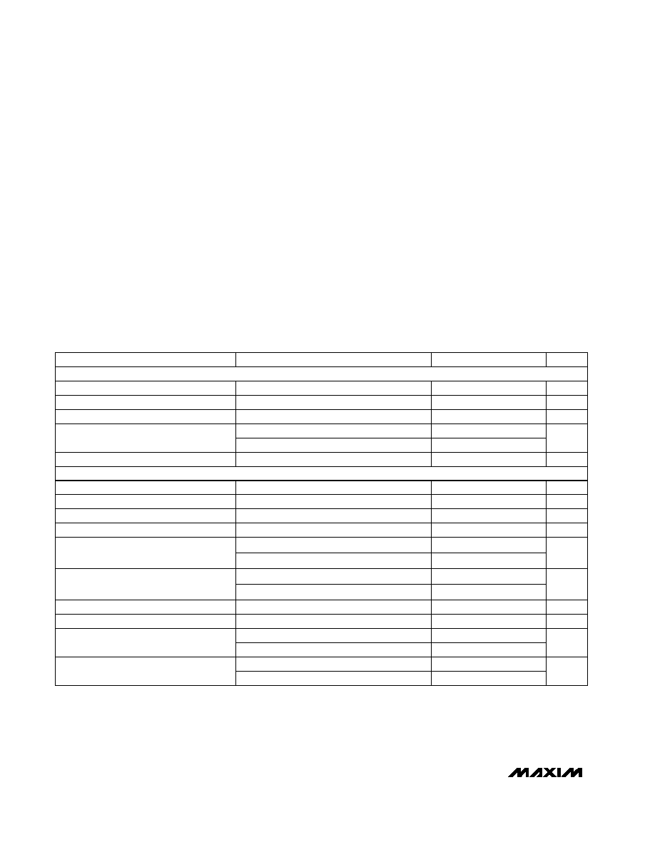
Typical Operating Circuit
19-1182; Rev 3; 10/01
PART
MAX745EAP
40∞C to +85∞C
TEMP RANGE
PIN-PACKAGE
20 SSOP
EVALUATION KIT MANUAL
FOLLOWS DATA SHEET
Ordering Information
Pin Configuration appears at end of data sheet.
MAX745C/D
0∞C to +70∞C
Dice*
*Dice are tested at T
A
= +25∞C.
SMBus is a trademark of Intel Corp.
(UP TO 24V)
REF
DCIN
V
IN
BST
VL
DHI
DLO
LX
CS
BATT
CELL
COUNT
SELECT
SET PER
CELL VOLTAGE
WITH 1% RESISTORS
ON
OFF
VADJ
STATUS
SETI
CELL0
CELL1
CCI
PGND
GND
IBAT
CCV
N
N
I
CHARGE
R
SENSE
VOUT
1≠4 Li+ CELLS
(UP TO 18V)
MAX745
THM/SHDN
For pricing, delivery, and ordering information, please contact Maxim/Dallas Direct! at
1-888-629-4642, or visit Maxim's website at www.maxim-ic.com.
MAX745
Switch-Mode Lithium-Ion
Battery Charger
2
_______________________________________________________________________________________
ABSOLUTE MAXIMUM RATINGS
ELECTRICAL CHARACTERISTICS
(V
DCIN
= 18V, V
BATT
= 8.4V, T
A
= 0∞C to +85∞C. Typical values are at T
A
= +25∞C, unless otherwise noted.)
Stresses beyond those listed under "Absolute Maximum Ratings" may cause permanent damage to the device. These are stress ratings only, and functional
operation of the device at these or any other conditions beyond those indicated in the operational sections of the specifications is not implied. Exposure to
absolute maximum rating conditions for extended periods may affect device reliability.
DCIN to GND ............................................................-0.3V to 26V
BST, DHI to GND ......................................................-0.3V to 30V
BST to LX ....................................................................-0.3V to 6V
DHI to LX............................................(LX - 0.3V) to (BST + 0.3V)
LX to GND ................................................-0.3V to (DCIN + 0.3V)
VL to GND...................................................................-0.3V to 6V
CELL0, CELL1, IBAT, STATUS, CCI, CCV, REF, SETI,
VADJ, DLO, THM/SHDN to GND.................-0.3V to (VL + 0.3V)
BATT, CS to GND .....................................................-0.3V to 20V
PGND to GND..........................................................-0.3V to 0.3V
VL Current ...........................................................................50mA
Continuous Power Dissipation (T
A
= +70∞C)
SSOP (derate 8.00mW/∞C above +70∞C) ....................640mW
Operating Temperature Range ...........................-40∞C to +85∞C
Storage Temperature.........................................-60∞C to +150∞C
Lead Temperature (soldering, 10s) .................................+300∞C
6.0V < V
DCIN
< 24V, logic inputs = VL
VL < 3.2V, V
CS
= 12V
VL < 3.2V, V
BATT
= 12V
Output high or low
0 < I
REF
< 1mA
6.0V < V
DCIN
< 24V, no load
T
A
= +25∞C
Output high or low
CONDITIONS
V
0
19
BATT, CS Input Voltage Range
µA
5
CS Input Current
µA
5
BATT Input Current
6
14
DLO On-Resistance
4
7
DHI On-Resistance
mA
4
6
DCIN Quiescent Supply Current
V
6
24
DCIN Input Voltage Range
%
89
93
DHI Maximum Duty Cycle
kHz
270
300
330
Oscillator Frequency
mV/mA
10
20
REF Output Load Regulation
V
5.15
5.40
5.65
VL Output Voltage
V
4.17
4.2
4.23
REF Output Voltage
UNITS
MIN
TYP
MAX
PARAMETER
4V < V
BATT
< 16V
6.0V < V
DCIN
< 24V
(Note 1)
mV
±1.5
CS to BATT Offset Voltage
SETI = V
REF
(full scale)
mV
170
185
205
CS to BATT
Current-Sense Voltage
Not including VADJ resistor tolerance
%
-0.65
+0.65
Absolute Voltage Accuracy
With 1% tolerance VADJ resistors
4.16
4.2
4.24
-0.75
+0.75
SWITCHING REGULATOR
SUPPLY AND REFERENCE
VL > 5.15V, V
BATT
= 12V
VL > 5.15V, V
CS
= 12V
400
500
SETI = 400mV
14
18
22

MAX745
_______________________________________________________________________________________
3
Switch-Mode Lithium-Ion
Battery Charger
Note 1: When V
SETI
= 0V, the battery charger turns off.
ELECTRICAL CHARACTERISTICS (continued)
(V
DCIN
= 18V, V
BATT
= 8.4V, T
A
= 0∞C to +85∞C. Typical values are at T
A
= +25∞C, unless otherwise noted.)
ELECTRICAL CHARACTERISTICS
(V
DCIN
= 18V, V
BATT
= 8.4V, T
A
= -40∞C to +85∞C, unless otherwise noted. Limits over temperature are guaranteed by design.)
6.0V < V
DCIN
< 24V
6.0V < V
DCIN
< 24V, no load
Output high or low
Output high or low
CONDITIONS
mV
165
205
CS to BATT Full-Scale
Current-Sense Voltage
Not including VADJ resistors
%
-1.0
+1.0
Absolute Voltage Accuracy
V
4.14
4.26
REF Output Voltage
V
5.10
5.70
VL Output Voltage
14
DLO On-Resistance
7
DHI On-Resistance
kHz
260
340
Oscillator Frequency
UNITS
MIN
TYP
MAX
PARAMETER
IBAT Compliance Voltage Range
0
2
V
V
IBAT
= 2V
IBAT Output Current vs.
Current-Sense Voltage
0.9
µA/mV
Charger in voltage-regulation mode,
V
STATUS
= 5V
STATUS Output Leakage Current
1
µA
Charger in current-regulation mode,
STATUS sinking 1mA
STATUS Output Low Voltage
0.2
V
THM/SHDN Falling Threshold
2.01
2.1
2.19
V
THM/SHDN Rising Threshold
2.20
2.3
2.34
V
1.1V < V
CCI
< 3.5V
CCV Clamp Voltage with Respect to CCI
PARAMETER
MIN
TYP
MAX
UNITS
GMV Amplifier Output Current
±130
µA
GMI Amplifier Transconductance
200
µA/V
GMI Amplifier Output Current
±320
µA
CCI Clamp Voltage with Respect to CCV
25
80 200
mV
25
80 200
mV
CELL0, CELL1 Input Bias Current
-1 +1
µA
SETI Input Voltage Range
0
V
REF
V
SETI, VADJ Input Bias Current
-10
+10
nA
VADJ Adjustment Range
10
%
CONDITIONS
VADJ Input Voltage Range
0 V
REF
1.1V < V
CCV
< 3.5V
V
(Note 1)
SWITCHING REGULATOR (Note 1)
SUPPLY AND REFERENCE
GMV Amplifier Transconductance
800
µA/V
CONTROL INPUTS/OUTPUTS
ERROR AMPLIFIERS

MAX745
Switch-Mode Lithium-Ion
Battery Charger
4
_______________________________________________________________________________________
4.5
0
0
0.1 0.2
0.4
1.0
BATTERY VOLTAGE
vs. CHARGING CURRENT
1.0
4.0
MAX745/TOC-01
CHARGING CURRENT (A)
BATTERY VOLTAGE (V)
0.3
0.5 0.6 0.7 0.8 0.9
3.0
2.0
0.5
3.5
2.5
1.5
R1 = 0.2
R16 = SHORT
R12 = OPEN CIRCUIT
200
0
0
0.5
1.5
4.0
CURRENT-SENSE VOLTAGE
vs. SETI VOLTAGE
40
160
MAX745/TOC-02
SETI VOLTAGE (V)
CURRENT-SENSE VOLTAGE (mV)
1.0
2.0
2.5
3.0
3.5
120
80
180
20
140
100
60
R1 = 0.2
4.45
3.95
0
0.5 1.0
2.0
4.5
VOLTAGE LIMIT
vs. VADJ VOLTAGE
4.05
4.35
MAX745/TOC-03
VADJ VOLTAGE (V)
PER-CELL VOLTAGE LIMIT (V)
1.5
2.5 3.0 3.5 4.0
4.25
4.15
4.40
4.00
4.30
4.20
4.10
4.205
4.195
0
25
50
REFERENCE VOLTAGE
vs. TEMPERATURE
4.197
4.203
MAX745/TOC-06
TEMPERATURE (∞C)
REFERENCE VOLTAGE (V)
75
100
4.201
4.199
4.204
4.196
4.202
4.200
4.198
__________________________________________Typical Operating Characteristics
(T
A
= +25∞C, V
DCIN
= 18V, V
BATT
= 4.2V, CELL0 = CELL1 = GND, C
VL
= 4.7µF C
REF
= 0.1µF. Circuit of Figure 1, unless otherwise
noted.)
5.50
0
0
5
10
25
VL LOAD REGULATION
5.10
5.40
MAX745/TOC-04
VL OUTPUT CURRENT (mA)
VL OUTPUT VOLTAGE (V)
15
20
5.30
5.20
5.45
5.05
5.35
5.25
5.15
4.25
4.15
0
500
1000
3000
REFERENCE LOAD REGULATION
4.17
4.23
MAX745/TOC-05
REFERENCE CURRENT (
µA)
REFERENCE VOLTAGE (V)
1500
2000
2500
4.21
4.19
4.24
4.16
4.22
4.20
4.18
_______________Detailed Description
The MAX745 is a switch-mode, Li+ battery charger that
can achieve 90% efficiency. The charge voltage and
current are set independently by external resistor-
dividers at SETI and VADJ, and at pin connections at
CELL0 and CELL1. VADJ is connected to a resistor-
divider to set the charging voltage. The output voltage-
adjustment range is ±5%, eliminating the need for 0.1%
resistors while still achieving 0.75% set accuracy using
1% resistors.
The MAX745 consists of a current-mode, pulse-width-
modulated (PWM) controller and two transconductance
error amplifiers: one for regulating current (GMI) and
the other for regulating voltage (GMV) (Figure 2). The
error amplifiers are controlled through the SETI and
VADJ pins. Whether the MAX745 is controlling voltage
or current at any time depends on the battery state. If
the battery is discharged, the MAX745 output reaches
the current-regulation limit before the voltage limit,
causing the system to regulate current. As the battery
charges, the voltage rises to the point where the volt-
age limit is reached and the charger switches to regu-
lating voltage. The STATUS pin indicates whether the
charger is regulating current or voltage.
Voltage Control
To set the voltage limit on the battery, connect a resis-
tor- divider to VADJ from REF. A 0V to V
REF
change at
VADJ sets a ±5% change in the battery limit voltage
around 4.2V. Since the 0 to 4.2V range on VADJ results
in only a 10% change on the voltage limit, the resistor-
divider's accuracy does not need to be as high as the
output voltage accuracy. Using 1% resistors for the
voltage dividers typically results in no more than 0.1%
degradation in output voltage accuracy. VADJ is inter-
nally buffered so that high-value resistors can be used
to set the output voltage. When the voltage at VADJ is
MAX745
Switch-Mode Lithium-Ion
Battery Charger
_______________________________________________________________________________________
5
______________________________________________________________Pin Description
IBAT
Current-Sense Amplifier's Analog Current-Source Output. See the Monitoring Charge Current section for a
detailed description.
2
DCIN
Charger Input Voltage. Bypass DCIN with a 0.1µF capacitor.
3
VL
Chip Power Supply. Output of the 5.4V linear regulator from DCIN. Bypass VL with a 4.7µF capacitor.
1
4
CCV
Voltage-Regulation-Loop Compensation Point
5
CCI
Current-Regulation-Loop Compensation Point
8
VADJ
Voltage-Adjustment Pin. VADJ is tied to a 1% tolerance external resistor-divider to adjust the voltage set
point by 10%, eliminating the need for precision 0.1% resistors. The input voltage range is 0V to V
REF
.
7
REF
4.2V Reference Voltage Output. Bypass REF with a 0.1µF or greater capacitor.
6
THM/
SHDN
Thermistor Sense-Voltage Input. THM/SHDN also performs the shutdown function. If pulled low,
the charger turns off.
13
STATUS
An open-drain MOSFET sinks current when in current-regulation mode, and is high impedance when in volt-
age-regulation mode. Connect STATUS to VL through a 1k
to 100k pullup resistor. STATUS can also drive
an LED for visual indication of regulation mode (see MAX745 EV kit). Leave STATUS floating if not used.
11, 12
CELL1,
CELL0
Logic Inputs to Select Cell Count. See Table 1 for cell-count programming.
10
GND
Analog Ground
9
SETI
SETI is externally tied to the resistor-divider between REF and GND to set the charging current.
14
BATT
Battery-Voltage-Sense Input and Current-Sense Negative Input
15
CS
Current-Sense Positive Input
16
PGND
Power Ground
17
DLO
Low-Side Power MOSFET Driver Output
18
DHI
High-Side Power MOSFET Driver Output
19
LX
Power Connection for the High-Side Power MOSFET Source
20
BST
Power Input for the High-Side Power MOSFET Driver
NAME
FUNCTION
PIN