 | ÐлекÑÑоннÑй компоненÑ: MAX791CPE | СкаÑаÑÑ:  PDF PDF  ZIP ZIP |
Äîêóìåíòàöèÿ è îïèñàíèÿ www.docs.chipfind.ru
MAX791
Microprocessor Supervisory Circuit
________________________________________________________________
Maxim Integrated Products
1
Call toll free 1-800-998-8800 for free samples or literature.
19-0075; Rev. 5; 7/95
_____________________
General Description
The MAX791 microprocessor (µP) supervisory circuit
reduces the complexity and number of components need-
ed to monitor power-supply and battery-control functions
in µP systems. The 50µA supply current makes the
MAX791 ideal for use in portable equipment, while the 6ns
chip-enable propagation delay and 250mA output capa-
bility (25mA in battery-backup mode) make it suitable for
larger, higher-performance equipment.
The MAX791 comes in 16-pin DIP and narrow SO pack-
ages and provides the following functions:
1) µP reset--
R
--
E
--
S
--
E
--
T
output is asserted during power-up,
power-down, and brownout conditions, and is guaran-
teed to be in the correct state for V
CC
down to 1V,
even with no battery in the circuit.
2) Manual-reset input.
3) A 1.25V threshold detector provides for power-fail
warning and low-battery detection, or monitors a
power supply other than +5V.
4) Two-stage power-fail warning--a separate low-line
comparator compares V
CC
to a threshold 150mV
above the reset threshold.
5) Backup-battery switchover for CMOS RAM, real-time
clocks, µPs, or other low-power logic.
6) Software monitoring of backup-battery voltage.
7) A watchdog-fault output is asserted if the watchdog
input has not been toggled within either a preset or
an adjustable timeout period.
8) Write protection of CMOS RAM or EEPROM.
9) Pulsed watchdog output, to give advance warning of
impending
W
--
D
--
O
assertion caused by watchdog timeout.
________________________Applications
Computers
Critical µP Power Monitoring
Controllers
Intelligent Instruments
Portable/Battery-Powered Equipment
____________________________Features
o
Precision 4.65V Voltage Monitoring
o
200ms Power-OK / Reset Time Delay
o
Independent Watchdog Timer--Preset or Adjustable
o
1µA Standby Current
o
Power Switching
250mA Output in V
CC
Mode
25mA Output in Battery-Backup Mode
o
On-Board Gating of Chip-Enable Signals
Memory Write-Cycle Completion
6ns CE Gate Propagation Delay
o
MaxCap
or SuperCap
Compatible
o
Voltage Monitor for Power-Fail or Low-Battery Warning
o
Backup-Battery Monitor
o
Guaranteed
R
--
E
--
S
--
E
--
T
Valid to V
CC
= 1V
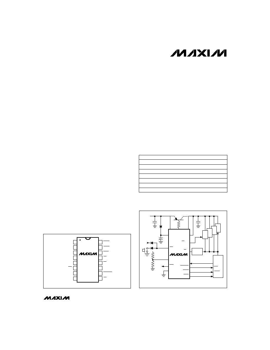
______________Ordering Information
16
15
14
13
12
11
10
9
1
2
3
4
5
6
7
8
WDPO
RESET
WDO
CE IN
GND
V
CC
V
OUT
VBATT
TOP VIEW
MAX791
CE OUT
WDI
LOWLINE
MR
SWT
PFI
PFO
BATT ON
DIP/SO
CMOS
RAM
MAX791
RESET
LOWLINE
WDI
CE IN
CE OUT
+5V
OTHER SYSTEM
RESET SOURCES
+12V
V
OUT
VBATT
*MaxCap
TM
A0A15
MR
+12V SUPPLY
FAILURE
BATT
ON
SWT
ADDRESS
DECODE
0.1
µ
F
0.1
µ
F
0.47F*
V
CC
PFI
PFO
GND
I/O
µ
P
NMI
INT
RESET
WDO
__________________Pin Configuration
__________Typical Operating Circuit
PART
TEMP. RANGE
PIN-PACKAGE
MAX791CPE
0°C to +70°C
16 Plastic DIP
MAX791CSE
0°C to +70°C
16 Narrow SO
MAX791C/D
0°C to +70°C
Dice*
MAX791EPE
-40°C to +85°C
16 Plastic DIP
MAX791ESE
-40°C to +85°C
16 Narrow SO
MAX791EJE
-40°C to +85°C
16 CERDIP
MAX791MJE
-55°C to +125°C
16 CERDIP
TM
MaxCap is a registered trademark of The Carborundum Corp.
TM
SuperCap is a registered trademark of Baknor Industries.
* Dice are specified at T
A
= +25°C.
MAX791
Microprocessor Supervisory Circuit
2
_______________________________________________________________________________________
Input Voltage (with respect to GND)
V
CC
.......................................................................-0.3V to +6V
VBATT..................................................................-0.3V to + 6V
All Other Inputs.....................................-0.3V to (V
OUT
+ 0.3V)
Input Current
V
CC
Peak ..........................................................................1.0A
V
CC
Continuous ............................................................250mA
VBATT Peak ..................................................................250mA
VBATT Continuous ..........................................................25mA
GND, BATT ON .............................................................100mA
All Other Outputs ............................................................25mA
Continuous Power Dissipation (T
A
= +70°C)
Plastic DIP (derate 10.53mW/°C above +70°C) ..........842mW
Narrow SO (derate 8.70mW/°C above +70°C) ............696mW
CERDIP (derate 10.00mW/°C above +70°C) ...............800mW
Operating Temperature Ranges
MAX791C_ _ ......................................................O°C to +70°C
MAX791E_ _ ....................................................-40°C to +85°C
MAX791MJE ..................................................-55°C to +125°C
Storage Temperature Range .............................-65°C to +160°C
Lead Temperature (soldering, 10sec) .............................+300°C
ELECTRICAL CHARACTERISTICS
(V
CC
= 4.75V to 5.5V, VBATT = 2.8V, T
A
= T
MIN
to T
MAX
, unless otherwise noted.)
Stresses beyond those listed under "Absolute Maximum Ratings" may cause permanent damage to the device. These are stress ratings only, and functional
operation of the device at these or any other conditions beyond those indicated in the operational sections of the specifications is not implied. Exposure to
absolute maximum rating conditions for extended periods may affect device reliability.
ABSOLUTE MAXIMUM RATINGS
PARAMETER
CONDITIONS
Supply Current in Battery-Backup
Mode (Excludes I
OUT
) (Note 2)
MIN
TYP
MAX
UNITS
VBATT = 4.5V, I
OUT
= 20mA
VBATT - 0.3
Operating Voltage Range
V
CC
, VBATT (Note 1)
0
5.5
V
V
CC
- 0.3
V
CC
- 0.2
V
CC
- 0.05 V
CC
- 0.02
VBATT-to-V
OUT
On-Resistance
5
VBATT = 2.0V
µA
17
30
Battery-Switchover Threshold
Power down
VBATT - 0.03
V
V
OUT
in Normal
Operating Mode
V
CC
= 3V, VBATT = 2.8V, I
OUT
= 100mA
V
CC
- 0.2
V
CC
- 0.12
V
V
CC
= 4.5V
0.8
1.6
0.8
1.2
V
CC
= 4.5V
V
CC
- 0.40
VBATT = 2.8V, I
OUT
= 10mA
VBATT - 0.25
0.04
1
Supply Current in Normal
Operating Mode (Excludes I
OUT
)
V
CC
> VBATT - 1V
50
150
µA
V
CC
-to-V
OUT
On-Resistance
V
CC
= 3V
1.2
2.0
VBATT = 4.5V
8
15
VBATT = 2.8V
Power up
13
25
VBATT + 0.03
V
OUT
in Battery-Backup Mode
VBATT = 2.0V, I
OUT
= 5mA
VBATT - 0.15
V
Battery-Switchover Hysteresis
60
mV
Low-Battery Detector Threshold
2
V
I
OUT
= 250mA
I
OUT
= 25mA
MAX791C/E
MAX791M
MAX791C/E
MAX791M
V
CC
< VBATT - 1.2V,
VBATT = 2.8V
T
A
= +25°C
T
A
= T
MIN
to T
MAX
VBATT Standby Current
(Note 3)
T
A
= T
MIN
to T
MAX
T
A
= +25°C
-1.0
0.02
µA
VBATT + 0.2V
V
CC
-0.1
0.02
ns
MAX791
Microprocessor Supervisory Circuit
_______________________________________________________________________________________
3
ELECTRICAL CHARACTERISTICS (continued)
(V
CC
= 4.75V to 5.5V, VBATT = 2.8V, T
A
= T
MIN
to T
MAX
, unless otherwise noted.)
0.7
1.5
I
SINK
= 25mA
mA
7
20
Output source current
W
--
D
--
P
--
O
Output
Short-Circuit Current
V
0.1
0.4
I
SINK
= 3.2mA
BATT ON Output
Low Voltage
ms
10
4.7nF capacitor connected from SWT to GND
Minimum Watchdog
Timeout Period
ms
1
W
--
D
--
P
--
O
Pulse Width
ns
100
V
IL
= 0.8V, V
IH
= 0.75 x V
CC
Minimum Watchdog Input
Pulse Width
µs
80
Power down
V
CC
-to-
L
--
O
--
W
--
--
L
--
I
--
N
--
E
Delay
sec
1.0
1.6
2.25
SWT connected to V
OUT
V
4.50
4.65
4.75
R
--
E
--
S
--
E
--
T
Threshold Voltage
mV
150
L
--
O
--
W
--
--
L
--
I
--
N
--
E
-to-
R
--
E
--
S
--
E
--
T
Threshold Voltage
µs
100
Power down
V
CC
-to-
R
--
E
--
S
--
E
--
T
Delay
mV
15
R
--
E
--
S
--
E
--
T
Threshold Hysteresis
Watchdog Timeout Period
ns
70
W
--
D
--
P
--
O
-to-
W
--
D
--
O
Delay
µA
ms
1
15
100
Source current
BATT ON Output
Short-Circuit Current
mA
60
Sink current
140
200
280
Power up
UNITS
MIN
TYP
MAX
R
--
E
--
S
--
E
--
T
Active Timeout Period
CONDITIONS
PARAMETER
0.004
0.3
MAX791E/M, I
SINK
= 50µA, V
CC
= 1.2V, V
CC
falling
0.1
0.4
I
SINK
= 3.2mA, V
CC
= 4.25V
V
3.5
I
SOURCE
= 1.6mA, V
CC
= 5V
R
--
E
--
S
--
E
--
T
Output Voltage
mA
7
20
Output source current
R
--
E
--
S
--
E
--
T
Output
Short-Circuit Current
0.4
I
SINK
= 3.2mA, V
CC
= 4.25V
µA
15
100
Output source current
L
--
O
--
W
--
--
L
--
I
--
N
--
E
Output
Short-Circuit Current
V
3.5
I
SOURCE
= 1µA, V
CC
= 5V
L
--
O
--
W
--
--
L
--
I
--
N
--
E
Output Voltage
0.4
I
SINK
= 3.2mA
mA
3
10
Output source current
W
--
D
--
O
Output Short-Circuit Current
V
3.5
I
SOURCE
= 500µA, V
CC
= 5V
W
--
D
--
O
Output Voltage
0.4
I
SINK
= 3.2mA
V
3.5
I
SOURCE
= 1mA
W
--
D
--
P
--
O
Output Voltage
0.004
0.3
MAX791C, I
SINK
= 50µA, V
CC
= 1.0V, V
CC
falling
RESET, LOW-LINE AND WATCHDOG TIMER
MAX791
Microprocessor Supervisory Circuit
4
_______________________________________________________________________________________
ELECTRICAL CHARACTERISTICS (continued)
(V
CC
= 4.75V to 5.5V, VBATT = 2.8V, T
A
= T
MIN
to T
MAX
, unless otherwise noted.)
Note 1:
Either V
CC
or VBATT can go to 0V, if the other is greater than 2.0V.
Note 2:
The supply current drawn by the MAX791 from the battery (excluding I
OUT
) typically goes to 10µA when
(VBATT - 1V) < V
CC
< VBATT. In most applications, this is a brief period as V
CC
falls through this region.
Note 3:
"+" = battery-discharging current, "-" = battery-charging current.
Note 4:
WDI is internally connected to a voltage divider between V
OUT
and GND. If unconnected, WDI is driven to 1.6V (typ),
disabling the watchdog function.
Note 5:
The chip-enable resistance is tested with V
CC
= 4.75V V
C
--
E
IN
= V
C
--
E
OUT
= V
CC
/ 2.
Note 6:
The chip-enable propagation delay is measured from the 50% point at
C
--
E
IN to the 50% point at
C
--
E
OUT.
ns
6
10
50
source impedance driver, C
LOAD
= 50pF
C
--
E
IN-to-C
--
E
OUT Propagation
Delay (Note 6)
-50
-10
WDI = 0V
µA
20
50
WDI = V
OUT
WDI Input Current
0.75 x V
CC
V
IH
µA
23
250
M
--
R
= 0V
M
--
R
Pull-Up Current
µs
7
75
150
Enabled mode
M
--
R
-to -
R
--
E
--
S
--
E
--
T
Propagation Delay
C
--
E
IN-to-
C
--
E
OUT Resistance
(Note 5)
µA
±0.005
±1
Disabled mode
C
--
E
IN Leakage Current
µs
15
Power down
R
--
E
--
S
--
E
--
T
-to-
C
--
E
OUT Delay
nA
±0.01
±25
PFI Leakage Current
V
1.25
V
CC
= 5V
M
--
R
Threshold
mA
0.1
0.75
2.0
µs
Disabled mode,
C
--
E
OUT = 0V
25
15
C
--
E
OUT Short-Circuit Current
(Reset Active)
V
1.20
1.25
1.30
V
CC
= 5V
PFI Input Threshold
V
0.8
V
IL
WDI Threshold Voltage
(Note 4)
UNITS
MIN
TYP
MAX
M
--
R
Minimum Pulse Width
CONDITIONS
PARAMETER
0.4
I
SINK
= 3.2mA
V
3.5
I
SOURCE
= 1µA, V
CC
= 5V
P
--
F
--
O
Output Voltage
mA
60
Output sink current
µA
1
15
100
Output source current
P
--
F
--
O
Short-Circuit Current
µs
55
V
IN
= 20mV, V
OD
= 15mV
PFI-to-
P
--
F
--
O
Delay
15
V
IN
= -20mV, V
OD
= 15mV
3.5
V
CC
= 5V, I
OUT
= -100µA
V
2.7
V
CC
= 0V, VBATT = 2.8V, I
OUT
= 1µA
C
--
E
OUT Output Voltage High
(Reset Active)
POWER-FAIL COMPARATOR
CHIP-ENABLE GATING
MANUAL RESET INPUT
MAX791
Microprocessor Supervisory Circuit
58
38
-60
-30
30
150
V
CC
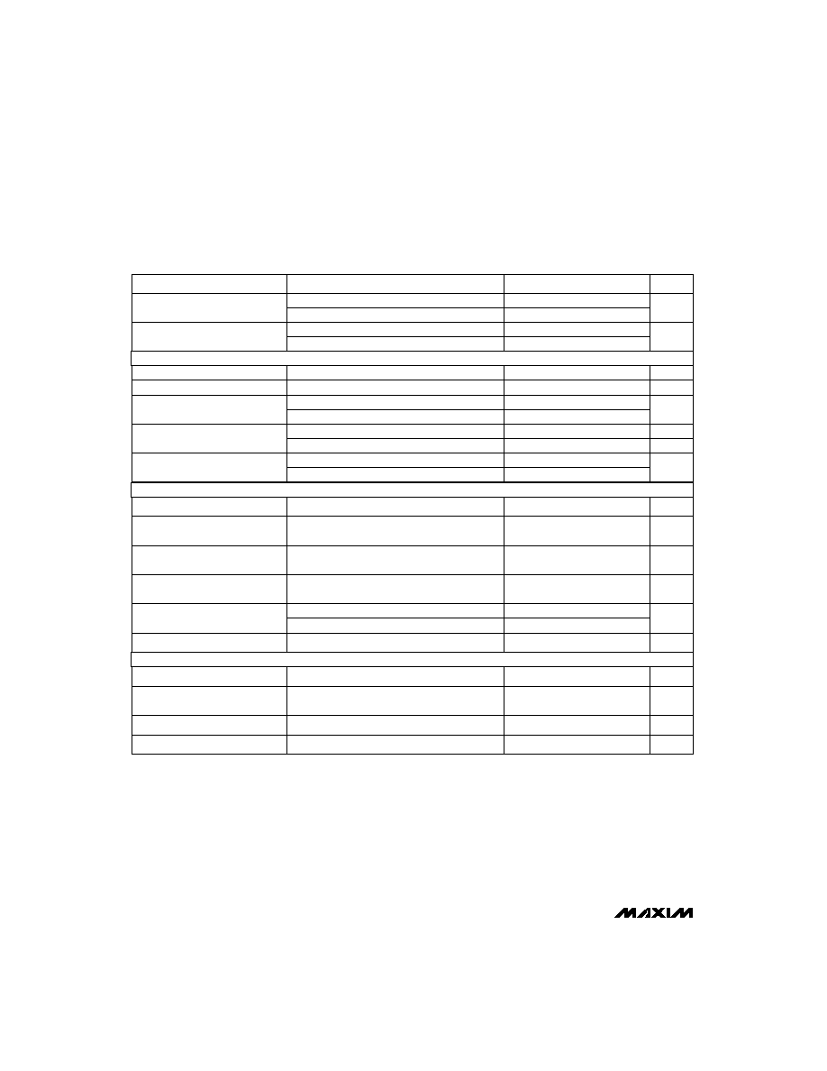
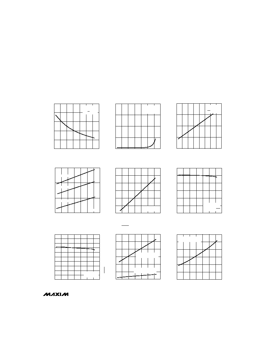
SUPPLY CURRENT vs. TEMPERATURE
(NORMAL OPERATING MODE)
42
54
MAX791-01
TEMPERATURE (°C)
V
CC
SUPPLY CURRENT (
µ
A)
0
120
90
60
46
50
V
CC
= +5V
VBATT = 2.8V
PFI, CE IN = 0V
4.80
4.30
4.40
4.35
-60
-30
30
150
RESET THRESHOLD
vs. TEMPERATURE
MAX791-07
TEMPERATURE (°C)
RESET THRESHOLD (V)
0
120
90
60
4.45
4.50
4.55
4.60
4.65
4.70
4.75
VBATT = 0V,
POWER DOWN
600
0
100
-60
-30
30
150
RESET OUTPUT RESISTANCE
vs. TEMPERATURE
MAX791-08
TEMPERATURE (°C)
RESET OUTPUT RESISTANCE (
)
0
120
90
60
200
300
400
500
V
CC
= 0V, VBATT = 2.8V
SINKING CURRENT
V
CC
= +5V, VBATT = 2.8V
SOURCING CURRENT
230
170
180
-60
-30
30
150
RESET DELAY
vs. TEMPERATURE
MAX791-09
TEMPERATURE (°C)
RESET DELAY (ms)
0
120
90
60
190
200
210
220
V
CC
= 0V TO 5V STEP
VBATT = 2.8V
__________________________________________Typical Operating Characteristics
(T
A
= +25°C, unless otherwise noted.)
20
5
-60
-30
30
150
VBATT-to-V
OUT
ON-RESISTANCE
vs. TEMPERATURE
MAX791-04
TEMPERATURE (°C)
VBATT-to-V
OUT
ON-RESISTANCE (
)
0
120
90
60
10
15
VBATT = 2.0V
VBATT = 2.8V
VBATT = 4.5V
V
CC
= 0V
2
0
-60
-30
30
150
BATTERY SUPPLY CURRENT vs. TEMPERATURE
(BATTERY-BACKUP MODE)
0.5
MAX791-02
TEMPERATURE (°C)
BATTERY SUPPLY CURRENT (
µ
A)
0
120
90
60
1
1.5
V
CC
= 0V
VBATT = 2.8V
NO LOAD
120
40
-60
-30
30
150 180
CHIP-ENABLE ON-RESISTANCE
vs. TEMPERATURE
60
MAX791-03
TEMPERATURE (°C)
CE ON-RESISTANCE (
)
0
120
90
60
80
100
V
CC
= +4.75V
VBATT = 2.8V
CE IN = V
CC
/2
1.2
0.6
0.7
-60
-30
30
150
V
CC
-to-V
OUT
ON-RESISTANCE
vs. TEMPERATURE
MAX791-05
TEMPERATURE (°C)
V
CC
-to-V
OUT
ON-RESISTANCE (
)
0
120
90
60
0.8
0.9
1.0
1.1
V
CC
= +5V,
VBATT = 0V
1.50
0
0.25
-60
-30
30
150
PFI THRESHOLD
vs. TEMPERATURE
MAX791-05
TEMPERATURE (°C)
PFI THRESHOLD (V)
0
120
90
60
0.50
0.75
1.00
1.25
V
CC
= +5V,
VBATT = 0V,
NO LOAD ON PFO
_______________________________________________________________________________________
5