 | –≠–Ľ–Ķ–ļ—ā—Ä–ĺ–Ĺ–Ĺ—č–Ļ –ļ–ĺ–ľ–Ņ–ĺ–Ĺ–Ķ–Ĺ—ā: MAX8215 | –°–ļ–į—á–į—ā—Ć:  PDF PDF  ZIP ZIP |
_______________General Description
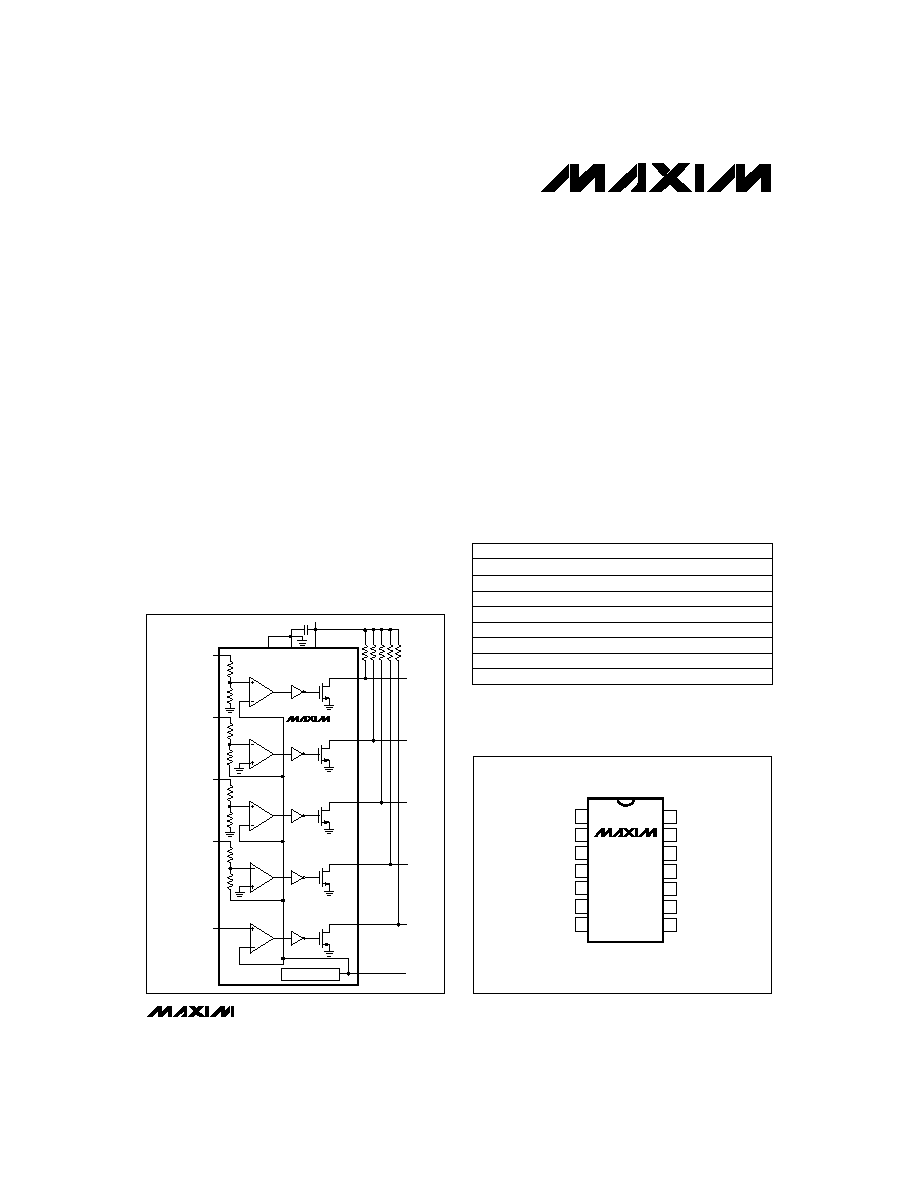
The MAX8215 contains five voltage comparators; four
are for monitoring +5V, -5V, +12V, and -12V, and the
fifth monitors any desired voltage. The MAX8216 is
identical, except it monitors Ī15V supplies instead of
Ī12V. The resistors required to monitor these voltages
and provide comparator hysteresis are included on-
chip. All comparators have open-drain outputs. These
devices consume 250ĶA max supply current over tem-
perature.
________________________Applications
Microprocessor Voltage Monitor
+5V, -5V, +12V, -12V Supply Monitoring (MAX8215)
+5V, -5V, +15V, -15V Supply Monitoring (MAX8216)
Overvoltage/Undervoltage Detection with
Uncommitted Comparator
Industrial Controllers
Mobile Radios
Portable Instruments
Industrial Equipment
Data-Acquisition Systems
____________________________Features
o
4 Dedicated Comparators plus 1 Auxiliary
Comparator
o
5V Dedicated Comparator Has Ī1.25% Accuracy
o
-5V, +12V, -12V, +15V, -15V Dedicated
Comparators Have Ī1.5% Accuracy
o
Overvoltage/Undervoltage Detection or
Programmable Delay Using Auxiliary Comparator
o
Internal 1.24V Reference with Ī1% Initial
Accuracy
o
Wide Supply Range: 2.7V to 11V
o
Built-In Hysteresis
o
250ĶA Max Supply Current Over Temp.
o
Independent Open-Drain Outputs
o
All Precision Components Included
______________Ordering Information
Ordering Information continued on last page.
*Dice are tested at T
A
= +25įC.
MAX8215/MAX8216
Ī5V, Ī12V (Ī15V) Dedicated
Microprocessor Voltage Monitors
________________________________________________________________
Maxim Integrated Products
1
1
2
3
4
14
13
12
11
V
DD
OUT1
OUT2
OUT3
-5V
+5V
GND
VREF
DIP/SO
TOP VIEW
MAX8215
MAX8216
5
6
7
10
9
8
OUT4
DOUT
PGND
DIN
-12V (-15V)
+12V (+15V)
( ) ARE FOR MAX8216 ONLY.
__________________Pin Configuration
+5V
OUT1
+5V
V
DD
PGND
GND
0.1
Ķ
F
-5V
OUT2
OUT3
+12V (+15V)
OUT4
-12V (-15V)
DOUT
DIN
1.24V REFERENCE
VREF
( ) ARE FOR
MAX8216 ONLY.
MAX8215
MAX8216
__________Typical Operating Circuit
Call toll free 1-800-998-8800 for free samples or literature.
PART
TEMP. RANGE
PIN-PACKAGE
MAX8215
CPD
0įC to +70įC
14 Plastic DIP
MAX8215CSD
0įC to +70įC
14 SO
MAX8215C/D
0įC to +70įC
Dice*
MAX8215ESD
-40įC to +85įC
14 SO
MAX8215EPD
-40įC to +85įC
14 Plastic DIP
MAX8215EJD
-40įC to +85įC
14 CERDIP
-55įC to +125įC
14 CERDIP
MAX8215MPD
-55įC to +125įC
14 Plastic DIP
MAX8215MJD
19-0169; Rev 0; 8/93
MAX8215/MAX8216
Ī5V, Ī12V (Ī15V) Dedicated
Microprocessor Voltage Monitors
2
_______________________________________________________________________________________
ABSOLUTE MAXIMUM RATINGS
ELECTRICAL CHARACTERISTICS
(V
DD
= +5V, GND = 0V, T
A
= T
MIN
to T
MAX
, unless otherwise noted.)
Stresses beyond those listed under "Absolute Maximum Ratings" may cause permanent damage to the device. These are stress ratings only, and functional
operation of the device at these or any other conditions beyond those indicated in the operational sections of the specifications is not implied. Exposure to
absolute maximum rating conditions for extended periods may affect device reliability.
PARAMETER
MIN
TYP
MAX
UNITS
Load Current
40
ĶA
-2.5
2.5
-1.75
1.75
I
DD
Supply Current
137
250
ĶA
Load Regulation
3.3
ĶV/ĶA
Line Regulation
0.01
%/V
Output Tempco
15
ppm/įC
2.7
11
V
DD
Supply Voltage Range
2.85
11
V
4.521
4.579
4.636
4.500
4.657
4.500
4.657
4.464
4.693
CONDITIONS
T
A
= T
MIN
to T
MAX
V
DD
............................................................................-0.3V, +12V
VREF..............................................................-0.3V, (V
DD
+ 0.3V)
OUT_, DOUT Outputs....................................-0.3V, (V
DD
+ 0.3V)
+5V Input...................................................................+20V, -0.3V
-5V, +12V, +15V, -12V, -15V Inputs.....................................Ī50V
DIN Input .......................................................(V
DD
+ 0.3V), -0.3V
Continuous Power Dissipation (T
A
= +70įC)
Plastic DIP (derate 10.00mW/įC above +70įC) ...........800mW
SO (derate 8.33mW/įC above +70įC) ..........................667mW
CERDIP (derate 9.09mW/įC above +70įC) ..................727mW
Operating Temperature Ranges:
MAX821_C_ _ ......................................................0įC to +70įC
MAX821_E_ _....................................................-40įC to +85įC
MAX821_M_ _ .................................................-55įC to +125įC
Storage Temperature Range .............................-65įC to +165įC
Lead Temperature (soldering, 10sec) .............................+300įC
MAX821_C
MAX821_E
MAX821_M
-1.00
1.00
MAX821_E/M
V
IN
decreasing, T
A
= +25įC
MAX821_C
MAX821_E
MAX821_M
4.636
4.749
1.25
V
IN
increasing
T
A
= +25įC
T
A
= +125įC
1.75
0.8
V
T
A
= -55įC
10.431
10.590
10.749
10.404
10.775
V
IN
decreasing (MAX8215 only), T
A
= +25įC
MAX821_C
MAX821_E
10.378
10.802
10.325
10.855
MAX821_M
V
T
A
= T
MIN
to T
MAX
+12V Trip Level
%
+5V Trip Level Hysteresis
Output Voltage Tolerance
Referred to 1.24V
%
-1.5
1.5
T
A
= +25įC
MAX821_C
T
A
= T
MIN
to T
MAX
+5V Trip Level
13.036
13.235
13.434
13.003
13.467
V
IN
decreasing (MAX8216 only), T
A
= +25įC
MAX821_C
MAX821_E
12.970
13.500
12.904
13.566
MAX821_M
V
T
A
= T
MIN
to T
MAX
+15V Trip Level
POWER SUPPLY
REFERENCE OUTPUT
COMPARATOR INPUTS
MAX8215/MAX8216
Ī5V, Ī12V (Ī15V) Dedicated
Microprocessor Voltage Monitors
_______________________________________________________________________________________
3
ELECTRICAL CHARACTERISTICS (continued)
(V
DD
= +5V, GND = 0V, T
A
= T
MIN
to T
MAX
, unless otherwise noted.)
PARAMETER
MIN
TYP
MAX
UNITS
MAX821_C
MAX821_E
-10.378
-10.802
-10.325
-10.855
1.25
2.00
Threshold Hysteresis
1.60
2.25
%
MAX821_M
130
168
CONDITIONS
T
A
= T
MIN
to T
MAX
+15V trip level
-5V trip level
-12V Trip Level
V
I V
IN
I decreasing, T
A
= +25įC
-13.003
-13.467
-15V Trip Level
I V
IN
I decreasing (MAX8216 only), T
A
= +25įC
V
MAX821_C
MAX821_E
-12.970
-13.500
-12.904
-13.566
MAX821_M
T
A
= T
MIN
to T
MAX
-4.348
-4.415
-4.482
-4.337
-4.493
-5V Trip Level
I V
IN
I decreasing, T
A
= +25įC
V
MAX821_C
MAX821_E
-4.326
-4.500
-4.304
-4.525
MAX821_M
T
A
= T
MIN
to T
MAX
160
Input Resistance
190
k
T
A
= +25įC
-2.00
2.00
-1.75
1.75
-1.5
0
1.5
V
IN
decreasing, T
A
= +25įC
+5V input to GND
-5V input to REF
-12V/-15V input to REF
Trip Level with Respect to 1.24V
-2.50
2.50
%
Threshold Hysteresis
1.25
2.00
%
T
A
= +25įC
Input Bias Current
2
10
nA
T
A
= +25įC
MAX821_C
MAX821_E
MAX821_M
-10.431 -10.590 -10.749
-13.036 -13.235 -13.434
-10.404
-10.776
+12V/+15V input to GND
1.25
2.00
+12V trip level
1.50
2.25
-12V trip level
1.50
2.25
-15V trip level
Hysteresis Tempco, Ī15, Ī12, -5
%/įC
0.005
T
A
= +25įC
V
OL
; V
DD
= 5V, I
SINK
= 2mA
0.11
0.3
V
DD
= 1.5V, I
SINK
= 0.2mA
0.04
0.3
Voltage Output Low
V
DD
= 1.0V, I
SINK
= 0.1mA
0.10
V
Leakage Current
Off State
1.0
ĶA
Comparator Response Time
(All Comparators)
30mV overdrive (Note 1)
20
Ķs
Note 1:
To overdrive the +5V/+12V/+15V comparators with a 30mV overdrive voltage, use the formula 30mV
to determine the required input voltage. V
THR
is the threshold of the particular overdriven comparator. To overdrive the
-5V/-12V/-15V comparators use 30mV .
(
V
THR
1.24
)
I
V
THR
1.24
I
[
1+
]
AUXILIARY COMPARATOR INPUT

MAX8215/MAX8216
Ī5V, Ī12V (Ī15V) Dedicated
Microprocessor Voltage Monitors
4
_______________________________________________________________________________________
__________________________________________Typical Operating Characteristics
(T
A
=+25įC, unless otherwise noted.)
0
-60
COMPARATOR INPUT BIAS CURRENT
vs. TEMPERATURE
MAX8215-TOC1
TEMPERATURE (Cį)
INPUT BIAS CURRENT (nA)
-40 -20 0
20 40 60 80 100 120 140
0.5
1
1.5
2
2.5
3
3.5
4
V
DD
= 5V
0
2
COMPARATOR INPUT BIAS CURRENT
vs. SUPPLY VOLTAGE
MAX8215-TOC2
SUPPLY VOLTAGE (V)
INPUT BIAS CUREENT (nA)
0.2
0.4
0.6
0.8
1
1.2
1.4
1.6
2.5
3
3.5
4
4.5
5
T
A
= +25įC
0
0
OUTPUT VOLTAGE LOW
vs. OUTPUT SINK CURRENT
MAX8215-TOC3
VOL (V)
OUTPUT SINK CURRENT (mA)
2.0 0.4 0.6 0.8
1
1.2 1.4 1.6 1.8
0.5
5
1.5
10
20
25
30
35
2
T
A
= +25įC
T
A
= +125įC
T
A
= -55įC
2
SUPPLY CURRENT
vs. SUPPLY VOLTAGE
SUPPLY VOLTAGE (V)
SUPPLY CURRENT (ĶA)
3
4
5
7
8
9
10 11
125
12
130
135
140
145
150
155
MAX8215-TOC4
T
A
= +125įC
6
T
A
= +25įC
T
A
= -55įC
-5V PIN = -5V
-12V PIN = -5V
+5V PIN = +5V
+12V PIN = +12V
1.23
0
REFERENCE VOLTAGE
vs. REFERENCE SOURCE CURRENT
MAX8215-TOC5
REFERENCE SOURCE CURRENT (ĶA)
VREF,REFERENCE VOLTAGE (V)
1.231
1.232
1.233
1.234
1.235
1.236
1.237
1.238
50
100
150
200
250
300
T
A
= +125įC
T
A
= -55įC
T
A
= +25įC
V
DD
= 5V
1
REFERENCE VOLTAGE
vs. SUPPLY VOLTAGE
SUPPLY VOLTAGE (V)
VREF, REFERENCE VOLTAGE (V)
2
3
4
5
6
7
8
9
10
0.95
11
1
1.05
1.1
1.15
1.2
1.25
MAX8215-TOC6
T
A
= -55įC
NOTE: -55
į
C IS WORST CASE
CONDITION FOR REFERENCE
REGULATION AT LOW VOLTAGES.
-55
VREF OUTPUT VOLTAGE
vs. TEMPERATURE
TEMPERATURE (įC)
VREF, REFERENCE VOLTAGE (V)
-35 -15
5
45
65 85 105 125
1.232
1.233
1.234
1.235
1.236
1.237
1.238
MAX8215-TOC7
V
DD
= 5V
25
MAX8215/MAX8216
Ī5V, Ī12V (Ī15V) Dedicated
Microprocessor Voltage Monitors
_______________________________________________________________________________________
5
+5V RESPONSE WITH
Ī100mV INPUT EXCURSION AROUND TRIP LEVEL
8215/16 SCOPE1
+5V COMP
+5V PIN
OUT1
_____________________________Typical Operating Characteristics (continued)
(T
A
= +25įC, unless otherwise noted.)
-5V RESPONSE WITH
Ī100mV INPUT EXCURSION AROUND TRIP LEVEL
8215/16 SCOPE2
-5V COMP
+5V PIN
OUT1
DOUT OUTPUT VOLTAGE vs. SUPPLY VOLTAGE
R1 = 15k
, R2 = 40k (see Figure 4)
8215/16 SCOPE3
SUPPLY
VOLTAGE
DOUT
OUTPUT
VOLTAGE
DIN COMPARATOR RESPONSE
WITH 30mV OVERDRIVE
8215/16 SCOPE4
COMP
OUTPUT
COMP
INPUT
DIN COMPARATOR RESPONSE
WITH 50mV OVERDRIVE
8215/16 SCOPE5
COMP
OUTPUT
COMP
INPUT
DIN COMPARATOR RESPONSE
WITH 100mV OVERDRIVE
8215/16 SCOPE6
COMP
OUTPUT
COMP
INPUT