
SCOPE: PROGRAMMABLE VOLTAGE DETECTOR
Device Type Generic Number SMD Number
01
MAX8211(x)/883B 5962-9081101
02 MAX8212(x)/883B 5962-9081102
Case Outline(s). The case outlines shall be designated in Mil-Std-1835 and as follows:
Outline Letter Mil-Std-1835 Case Outline Package Code
Maxim SMD
JA P
GDIP1-T08 or CDIP2-T08 8 Lead CERDIP J08
FB X CDFP3-F10 10 Pin Flatpack F10
TV G MACY1-8X 8 Lead Can G99
Absolute Maximum Ratings
Supply Voltage .................................................................................................... -0.5 to +18V
Output Voltage .................................................................................................... -0.5 to +18V
Hysteresis Voltage ................................................... +0.5V to -18V with respect to V
+
+0.5V
Threshold Input Voltage ......................................................................... -0.5V to (V
+
+0.5V)
Current Into Any Terminal ..........................................................................................
±
50mA
Lead Temperature (soldering, 10 seconds) ....................................................................... +300
∞
C
Storage Temperature ........................................................................................... -65
∞
C to +150
∞
C
Continuous Power Dissipation .................................................................................. T
A
=
+
70
∞
C
8 lead CERDIP(derate 8.0mW/
∞
C above +70
∞
C) .......................................................... 640mW
10 lead Flatpack(derate 5.3mW/
∞
C above +70
∞
C) ........................................................ 421mW
8 lead Can(derate 6.67mW/
∞
C above +70
∞
C) ................................................................ 533mW
Junction Temperature T
J
.............................................................................................. +150
∞
C
Thermal Resistance, Junction to Case,
JC:
Case Outline 8 lead CERDIP.......................................................................... 55
∞
C/W
Case Outline 10 lead Flatpack ........................................................................ 85
∞
C/W
Case Outline 8 lead Can ................................................................................ 45
∞
C/W
Thermal Resistance, Junction to Ambient,
JA:
Case Outline 8 lead CERDIP....................................................................... 125
∞
C/W
Case Outline 10 lead Flatpack ...................................................................... 190
∞
C/W
Case Outline 8 lead Can .............................................................................. 150
∞
C/W
Recommended Operating Conditions
Ambient Operating Range (T
A
) ................................................................... -55
∞
C to
+
125
∞
C
Supply Voltage Range (V
+
) ............................................................................... 2.0V to 16.5V
Stresses beyond those listed under "Absolute Maximum Ratings" may cause permanent damage to the device.
These are stress ratings only, and functional operation of the device at these or any other conditions beyond
those indicated in the operational sections of the specifications is not implied. Exposure to absolute maximum
rating conditions for extended periods may affect device reliability.
----------------------------
Electrical Characteristics of MAX8211/8212/883B
19-3189
Rev. D
for /883B and SMD 5962-90811
Page 2 of
5
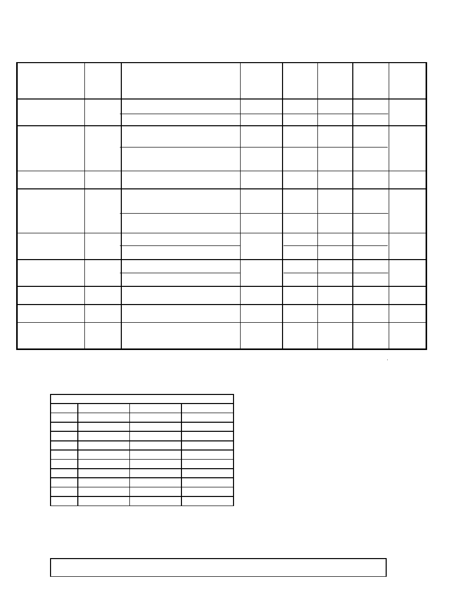
TABLE 1. ELECTRICAL TESTS:
TEST
Symbol
CONDITIONS
-55
∞
C <=T
A
<= +125
∞
C
V
+
=+5.0V
Unless otherwise specified
Group A
Subgroup
Device
type
Limits
Min
Limits
Max
Units
Supply Current
I
+
V
+
=2V, 5V, 16.5V, V
TH
=GND, V
+
V
+
=2.2V, 5V,16.5V, V
TH
=GND, V
+
1
2,3
All
15
20
µ
A
Threshold Trip
Voltage
V
THP
V
+
=16.5V, I
OUT
=4mA
V
+
=2.0V, I
OUT
=500
µ
A
V
+
=16.5V, I
OUT
=3mA
V
+
=2.2V, I
OUT
=500
µ
A
1
2,3
All
All
1.11
1.05
1.19
1.25
V
Threshold Input
Current
I
TH
V
TH
=GND, V
+
1
2,3
All
10
20
nA
Output Leakage
Current
I
OLK
V
OUT
=16.5V, V
TH
=1.3V
V
OUT
=5V, V
TH
=1.3V
V
OUT
=16.5V, V
TH
=0.9V
V
OUT
=5V, V
TH
=0.9V
1,2,3
1,2,3
01
02
30
10
30
10
µ
A
Output Saturation
Voltage
V
SAT
I
OUT
=2mA, V
TH
=1.0V
I
OUT
=2mA, V
TH
=1.3V
1
01
02
0.4
0.4
V
Maximum
Available Output
Current
I
OH
V
TH
=1.0V
V
TH
=1.3V
1,2,3
01
02
4.0
12
mA
Hysteresis Leakage
Current
I
HYS
V
+
=16.5V, V
HYS
=GND, V
TH
=0.9V
1,2,3
All
3
µ
A
Hysteresis
Saturation Voltage
V
HYS
(max)
I
HYS
=0.5mA, V
TH
=1.3V measured
with respect to V
+
1
All
-0.2 V
Maximum
Available
Hysteresis Current
I
HYS
(max)
V
TH
=1.3V, V
HYS
=0V
1
All
2
mA
NOTE 1: V
TH
8Vfor normal operation, except under stress testing.
TERMINAL CONNECTIONS:
For both MAX8211 and MAX8212
J8
F10
TO99
1
NC
NC
THRESH
2
HYST
HYST
OUT
3
THRESH
THRESH
NC
4
OUT
OUT
GND
5
GND
GND
NC
6
NC
NC
NC
7
NC
NC
V+(case)
8
V+
V+
HYST
9
NC
10
NC
----------------------------
Electrical Characteristics of MAX8211/8212/883B
19-3189
Rev. D
for /883B and SMD 5962-90811
Page 3 of
5
Device Type
Package
ORDERING INFORMATION:
SMD Number
01
8 pin CERDIP
MAX8211MJA/883B
5962-9081101MPA
01
10 lead Flatpack
MAX8211MFB/883B
5962-9081101MXC
01
8 pin Can
MAX8211MTV/883B
5962-9081101MGC
02
8 pin CERDIP
MAX8212MJA/883B
5962-9081202MPA
02
10 lead Flatpack
MAX8212MFB/883B
5962-9081202MXC
02
8 pin Can
MAX8212MTV/883B
5962-9081202MGC
QUALITY ASSURANCE
Sampling and inspection procedures shall be in accordance with MIL-Prf-38535, Appendix A as specified in Mil-
Std-883.
Screening shall be in accordance with Method 5004 of Mil-Std-883. Burn-in test Method 1015:
1. Test Condition, A, B, C, or D.
2. TA = +125
∞
C minimum.
3. Interim and final electrical test requirements shall be specified in Table 2.
Quality conformance inspection shall be in accordance with Method 5005 of Mil-Std-883, including Groups A, B,
C, and D inspection.
Group A inspection:
1. Tests as specified in Table 2.
2. Selected subgroups in Table 1, Method 5005 of Mil-Std-883 shall be omitted.
Group C and D inspections:
a. End-point electrical parameters shall be specified in Table 1.
b. Steady-state life test, Method 1005 of Mil-Std-883:
1. Test condition A, B, C, D.
2. TA = +125
∞
C, minimum.
3. Test duration, 1000 hours, except as permitted by Method 1005 of Mil-Std-883.
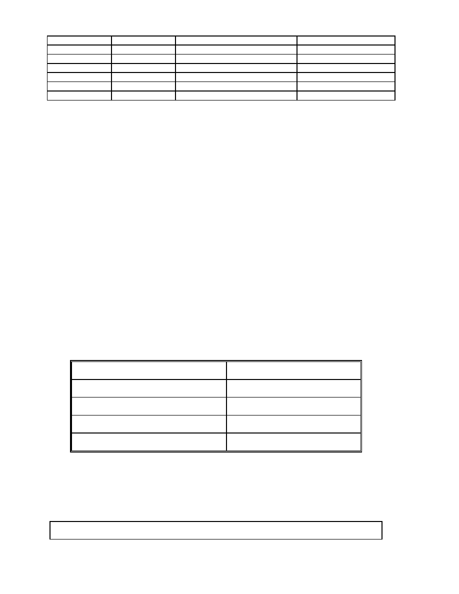
TABLE 2. ELECTRICAL TEST REQUIREMENTS
Mil-Std-883 Test Requirements
Subgroups
per Method 5005, Table 1
Interim Electric Parameters
Method 5004
1
Final Electrical Parameters
Method 5005
1*, 2, 3
Group A Test Requirements
Method 5005
1, 2, 3
Group C and D End-Point Electrical Parameters
Method 5005
1
* PDA applies to Subgroup 1 only.
----------------------------
Electrical Characteristics of MAX8211/8212/883B
19-3189
Rev. D
for /883B and SMD 5962-90811
Page 4 of
5