 | –≠–ª–µ–∫—Ç—Ä–æ–Ω–Ω—ã–π –∫–æ–º–ø–æ–Ω–µ–Ω—Ç: MAX8620Y | –°–∫–∞—á–∞—Ç—å:  PDF PDF  ZIP ZIP |
General Description
The MAX8620Y micro-power-management integrated
circuit (µPMIC) powers low-voltage microprocessors or
DSPs in portable devices. The µPMIC includes a high-
efficiency step-down DC-DC converter, two low-
dropout linear regulators (LDOs), a microprocessor
reset output, and power-on/off control logic. This device
maintains high efficiency at light loads with a low 115µA
supply current, and its miniature TDFN package makes
it ideal for portable devices.
The MAX8620Y's step-down DC-DC converter utilizes a
proprietary 4MHz hysteretic-PWM control scheme that
allows for ultra-small external components. Internal syn-
chronous rectification improves efficiency and elimi-
nates the external Schottky diode that is required in
conventional step-down converters. The output voltage
is adjustable from 0.6V to 3.3V, with guaranteed output
current up to 500mA.
The MAX8620Y's two LDOs offer low 45µV
RMS
output
noise and a low dropout of only 200mV at 200mA. Each
LDO delivers at least 300mA of continuous output cur-
rent. The output voltages are pin selectable from 1.8V
to 3.3V for flexibility.
A microprocessor reset output (RESET) monitors OUT1
and warns the system of impending power loss allow-
ing safe shutdown. RESET asserts during power-up,
power-down, shutdown, and fault conditions where
V
OUT1
is below its regulation voltage.
Applications
Cellular Handsets
Smart Phones/PDA Phones
PDAs
Wireless LAN
Microprocessor and DSP Solutions including
MSMTM, XScaleTM, ARMTM, and OMAPTM
Features
Three Regulators and a Reset in One Package
High-Efficiency Step-Down Converter
Up to 4MHz Fixed Switching Frequency
500mA Guaranteed Output Current
0.6V to 3.3V Adjustable Output Voltage
±2% Initial Accuracy
Fast Voltage-Positioning Transient Response
Internal Synchronous Rectifier
Two 300mA LDO Regulators
200mV Dropout at 200mA Load
Low 45µV
RMS
Output Noise
3% Accuracy over Line, Load, and Temperature
Overcurrent Protection
Nine Pin-Selectable Output-Voltage Settings
30ms (min) RESET Output Flag
2.7V to 5.5V Input
115µA (typ) Supply Current at No Load
Thermal-Overload Protection
Tiny 3mm x 3mm x 0.8mm TDFN Package
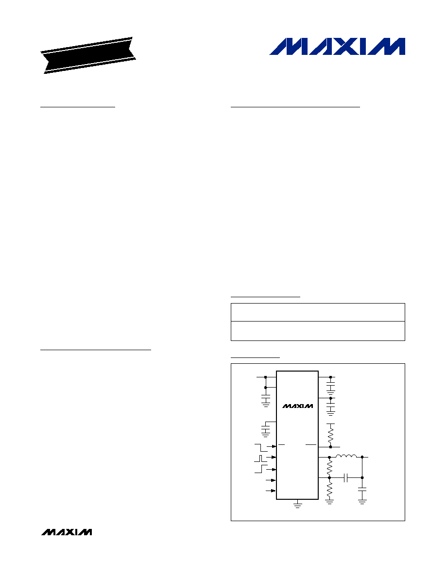
MAX8620Y
µPMIC for Microprocessors or DSPs
in Portable Equipment
________________________________________________________________ Maxim Integrated Products
1
Ordering Information
MAX8620Y
OUT1
V
IN
V
LOGIC
100k
RESET
OUT2
LX
FB
GND
IN2
BP
HF_PWR
PWR_ON
SEL1
RESET
SEL2
EN2
IN1
1.80V, 2.60V, 2.80V, 2.85V,
3.00V, OR 3.30V*
300mA
1.80V, 2.50V, 2.60V,
2.85V, OR 3.00V*
300mA
OUT3
0.6V TO 3.3V
500mA
*USE SEL1 AND SEL2 TO SET V
OUT1
AND V
OUT2
PART
TEMP RANGE
PIN-
PACKAGE
TOP
MARK
MAX8620YETD
-40∞C to +85∞C
14 TDFN-EP
(T1433-2)
AAB
Typical Operating Circuit
19-3564; Rev 0; 1/05
For pricing, delivery, and ordering information, please contact Maxim/Dallas Direct! at
1-888-629-4642, or visit Maxim's website at www.maxim-ic.com.
MSM is a trademark of QUALCOMM, Inc.
XScale is a trademark of Intel Corp.
ARM is a trademark of ARM Limited.
OMAP is a trademark of Texas Instruments, Inc.
EVALUATION KIT
AVAILABLE
Pin Configuration appears at end of data sheet.

MAX8620Y
µPMIC for Microprocessors or DSPs
in Portable Equipment
2
_______________________________________________________________________________________
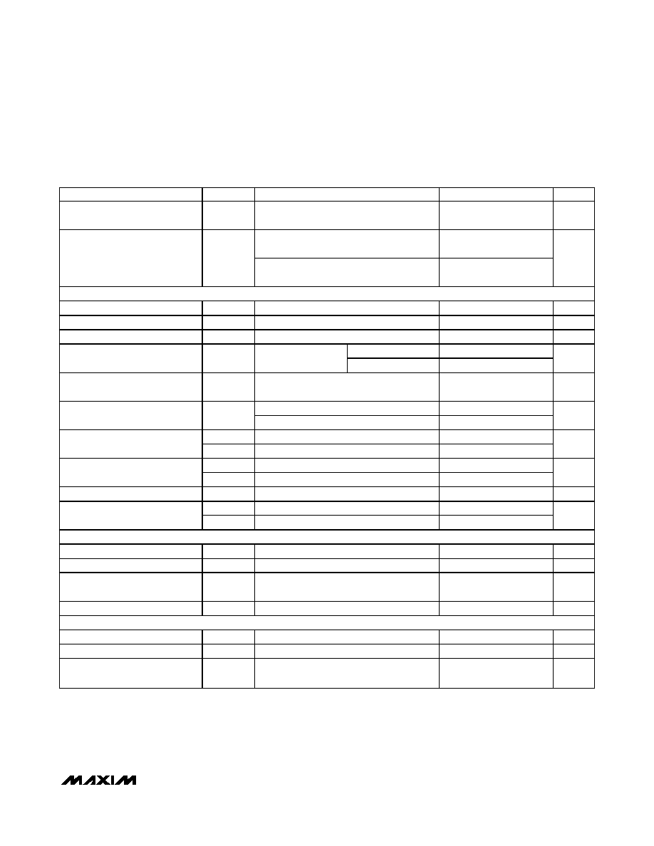
ABSOLUTE MAXIMUM RATINGS
ELECTRICAL CHARACTERISTICS
(V
IN1
= V
IN2
= +3.7V, C
IN
= 10µF, C
BP
= 0.01µF, T
A
= -40∞C to +85∞C, unless otherwise noted. Typical values are at T
A
= +25∞C.)
(Note 1)
Stresses beyond those listed under "Absolute Maximum Ratings" may cause permanent damage to the device. These are stress ratings only, and functional
operation of the device at these or any other conditions beyond those indicated in the operational sections of the specifications is not implied. Exposure to
absolute maximum rating conditions for extended periods may affect device reliability.
IN1, IN2, PWR_ON, RESET, EN2, SEL1, SEL2,
HF_PWR, FB, BP to GND ..................................-0.3V to +6.0V
OUT1, OUT2 to GND .................................-0.3V to (V
IN1
+ 0.3V)
LX Current ......................................................................1.5A
RMS
Continuous Power Dissipation (T
A
= +70∞C)
14-Pin TDFN (derate 18.2mW/∞C above +70∞C) .......1454mW
Operating Temperature Range ...........................-40∞C to +85∞C
Junction Temperature ......................................................+150∞C
Storage Temperature Range .............................-65∞C to +150∞C
Lead Temperature (soldering, 10s) .................................+300∞C
PARAMETER
SYMBOL
CONDITIONS
MIN
TYP
MAX
UNITS
Supply Voltage Range
V
IN1
2.7
5.5
V
Shutdown Supply Current
I
SHDN
V
IN1
= V
IN2
= 4.2V, PWR_ON = HF_PWR =
GND
5.5
10
µA
All outputs enabled, no load
115
140
Supply Current
I
IN1
+ I
IN2
V
OUT1
= V
OUT3
= 1.8V, I
OUT1
= I
OUT3
=
500µA, OUT2 disabled
430
µA
UNDERVOLTAGE LOCKOUT
V
IN1
= V
IN2
rising
2.70
2.85
3.05
UVLO Threshold
V
UVLO
V
IN1
= V
IN2
falling
2.35
V
THERMAL PROTECTION
Thermal-Shutdown Threshold
Temperature rising
+160
∞C
Thermal-Shutdown Hysteresis
15
∞C
REFERENCE (BP)
Reference Bypass Output
Voltage
V
BP
0
I
BP
1µA
1.231
1.250
1.269
V
LOGIC AND CONTROL INPUTS (PWR_ON, HF_PWR, EN2)
PWR_ON, HF_PWR, EN2 Input
Low Voltage
V
IL
V
IN1
= V
IN2
= 2.7V to 4.2V (Note 2)
0.4
V
PWR_ON, HF_PWR, EN2 Input
High Voltage
V
IH
V
IN1
= V
IN2
= 2.7V to 4.2V
(Note 2)
1.44
V
Input Bias Current
I
INB
V
PWR_ON
= V
HF_PWR
= V
EN2
= 0V or 5.5V
-1
+1
µA
HF_PWR Timer
t
HF
From the rising edge of HF_PWR until the
one-shot timer expires (Figure 4)
1.05
1.31
1.46
s
LINEAR REGULATORS (OUT1, OUT2)
0∞C to +85∞C
-1.3
+1.8
I
LOAD
= 1mA, 3.7V
V
IN
5.5V
-40∞C to +85∞C
-1.5
+1.8
1mA
I
LOAD
300mA
-1.2
OUT1, OUT2 Output-Voltage
Accuracy
V
OUT1
,
V
OUT2
I
LOAD
= 150mA
0
%
OUT1, OUT2 Output Current
I
OUT_
300
mA
OUT1, OUT2 Output Current Limit
I
LIM_
V
OUT_
= 0V
310
550
940
mA
OUT1, OUT2 Dropout Voltage
V
DO
I
LOAD
= 200mA, T
A
= +85∞C (Note 3)
200
380
mV
MAX8620Y
µPMIC for Microprocessors or DSPs
in Portable Equipment
_______________________________________________________________________________________
3
PARAMETER
SYMBOL
CONDITIONS
MIN
TYP
MAX
UNITS
OUT1, OUT2 Power-Supply
Rejection Ratio
f = 10Hz to 10kHz, C
OUT_
= 4.7µF,
I
LOAD_
= 30mA
60
dB
f = 100Hz to 100kHz, C
OUT_
= 4.7µF,
I
LOAD_
= 30mA
45
Output Noise Voltage
f = 100Hz to 100kHz, C
OUT_
= 4.7µF,
I
LOAD_
= 30mA, C
BP
open
100
µV
RMS
STEP-DOWN CONVERTER (OUT3)
Output Voltage Range
V
OUT3
0.6
3.3
V
FB Threshold Voltage
V
TH
V
FB
falling
0.6
V
FB Threshold Line Regulation
V
IN1
= V
IN2
= 2.7V to 5.5V (Note 2)
0.08
%/V
T
A
= +25∞C
-2
+2
FB Threshold Voltage Accuracy
(Falling) (% of V
TH
)
I
OUT3
= 0mA
T
A
= -40∞C to +85∞C
-3
+3
%
FB Threshold Voltage Hysteresis
(% of V
TH
)
V
HYS
2
%
OUT3 disabled
10
FB Bias Current
I
FB
V
FB
= 0.5V
10
µA
I
LIM3P
pFET switch
675
950
1200
Current Limit
I
LIM3N
nFET rectifier
875
1000
1200
mA
R
ONP
pFET switch, I
LX
= -200mA
0.65
1.5
On-Resistance
R
ONN
nFET rectifier, I
LX
= +200mA
0.35
0.8
Rectifier-Off Current Threshold
I
LXOFF
30
60
mA
t
ON
107
Minimum On- and Off-Times
t
OFF
95
ns
OPEN-DRAIN, ACTIVE-LOW RESET OUTPUT (RESET)
RESET Output-Voltage Low
V
OL
I
SINK
= 500µA
0.3
V
RESET Output Leakage Current
V
RESET
= 5.5V
100
nA
RESET Threshold Voltage
V
THR
Percent of the OUT1 regulation voltage
(Note 4)
84
87
90
%
RESET Timeout Period
t
RP
Figure 4
30
60
ms
LDO OUTPUT-VOLTAGE SELECT INPUTS (SEL1, SEL2)
SEL_ Input Low Threshold
1
V
SEL_ Input High Threshold
V
IN_
- 0.2V
V
SEL_ Input Bias Current
V
IN1
= V
IN2
= 4.2V, V
SEL1
= 0V or V
IN1
,
V
SEL2
= 0V or V
IN1
±0.1
µA
ELECTRICAL CHARACTERISTICS (continued)
(V
IN1
= V
IN2
= +3.7V, C
IN
= 10µF, C
BP
= 0.01µF, T
A
= -40∞C to +85∞C, unless otherwise noted. Typical values are at T
A
= +25∞C.)
(Note 1)
Note 1: Specifications are 100% production tested at T
A
= +25∞C. Maximum and minimum limits over temperature are guaranteed
by design and characterization.
Note 2: After startup.
Note 3: Guaranteed by design.
Note 4: RESET asserts low when V
OUT1
drops below the specified percent of the OUT1 regulation voltage.

MAX8620Y
µPMIC for Microprocessors or DSPs
in Portable Equipment
4
_______________________________________________________________________________________
Typical Operating Characteristics
(V
IN1
= V
IN2
= 3.7V, PWR_ON = IN1, L = 2.2µH (LQH31CN2R2M53), C
FF
= 150pF, V
OUT1
= V
OUT2
= 2.6V, V
OUT3
= 1.867V (R1 =
150k
, R2 = 75k), C
IN
= 10µF, C
BP
= 0.01µF, C
OUT1
= C
OUT2
= 4.7µF, C
OUT3
= 2.2µF, RESET pulled up with 100k
to OUT1,
T
A
= +25∞C, unless otherwise noted.)
EFFICIENCY vs. LOAD CURRENT
MAX8620Y toc01
LOAD CURRENT (mA)
EFFICIENCY (%)
100
10
1
10
20
30
40
50
60
70
80
90
100
0
0.1
1000
L = 4.7
µH
L = 2.2
µH
L = 1.0
µH
INPUT QUIESCENT CURRENT
vs. INPUT VOLTAGE
MAX8620Y toc02
INPUT VOLTAGE (V)
QUIESCENT CURRENT (
µ
A)
5.0
4.5
3.5
4.0
3.0
2.5
20
40
60
80
100
120
140
160
180
0
2.0
5.5
SWITCHING FREQUENCY vs. LOAD CURRENT
SWITCHING FREQUENCY (MHz)
450
400
350
300
250
200
150
100
50
1
10
0.1
0
500
MAX8620Y toc03
LOAD CURRENT (mA)
L = 4.7
µH
L = 2.2
µH
L = 1.0
µH
EFFICIENCY vs. OUTPUT VOLTAGE
OUTPUT VOLTAGE (V)
EFFICIENCY (%)
2.4
2.2
0.8 1.0 1.2
1.6 1.8
1.4
2.0
65
70
75
80
85
90
95
100
60
0.6
2.6
MAX8620Y toc04
L = 4.7
µH
L = 2.2
µH
L = 1.0
µH
LIGHT-LOAD SWITCHING WAVEFORMS
MAX8620Y toc05
200ns/div
I
L
V
OUT
AC-COUPLED
2V/div
20mV/div
100mA/div
V
LX
HEAVY-LOAD SWITCHING WAVEFORMS
MAX8620Y toc06
200ns/div
I
L
V
OUT
AC-COUPLED
2V/div
20mV/div
200mA/div
V
LX

MAX8620Y
µPMIC for Microprocessors or DSPs
in Portable Equipment
_______________________________________________________________________________________
5
Typical Operating Characteristics (continued)
(V
IN1
= V
IN2
= 3.7V, PWR_ON = IN1, L = 2.2µH (LQH31CN2R2M53), C
FF
= 150pF, V
OUT1
= V
OUT2
= 2.6V, V
OUT3
= 1.867V (R1 =
150k
, R2 = 75k), C
IN
= 10µF, C
BP
= 0.01µF, C
OUT1
= C
OUT2
= 4.7µF, C
OUT3
= 2.2µF, RESET pulled up with 100k
to OUT1,
T
A
= +25∞C, unless otherwise noted.)
LOAD TRANSIENT (50mA TO 300mA)
MAX8620Y toc07
2
µs/div
I
L
I
LOAD
V
OUT3
AC-COUPLED
50mV/div
200mA/div
300mA
50mA
200mA/div
POWER-UP WAVEFORMS
MAX8620Y toc08
40
µs/div
V
OUT3
V
OUT1
V
OUT2
V
IN
2V/div
1V/div
1V/div
1V/div
PWR_ON STARTUP/SHUTDOWN WAVEFORMS
MAX8620Y toc09
100
µs/div
V
OUT3
V
OUT1
V
OUT2
V
PWR_ON
2V/div
1V/div
1V/div
1V/div
RESET WAVEFORMS
MAX8620Y toc10
10ms/div
V
OUT1
V
PWR_ON
2V/div
1V/div
1V/div
V
RESET
OUT2 SHUTDOWN WAVEFORMS
MAX8620Y toc11
200
µs/div
V
OUT2
V
EN2
1V/div
1V/div
HF_PWR STARTUP WAVEFORMS
MAX8620Y toc12
10ms/div
V
OUT1
V
HF_PWR
1V/div
2V/div
1V/div
V
RESET