 | –≠–ª–µ–∫—Ç—Ä–æ–Ω–Ω—ã–π –∫–æ–º–ø–æ–Ω–µ–Ω—Ç: MAX868C/D | –°–∫–∞—á–∞—Ç—å:  PDF PDF  ZIP ZIP |

For free samples & the latest literature: http://www.maxim-ic.com, or phone 1-800-998-8800.
For small orders, phone 408-737-7600 ext. 3468.
General Description
The MAX868 inverting charge pump provides a low-cost
and compact means of generating a regulated negative
voltage up to -2 x V
IN
from a positive input voltage
between 1.8V and 5.5V. It uses a pulse-frequency-
modulation (PFM) control scheme to generate the regulat-
ed negative output voltage. PFM operation is obtained
by gating the internal 450kHz oscillator on and off as
needed to maintain output voltage regulation. This
unique on-demand switching scheme gives the MAX868
excellent light-load efficiency without degrading its full-
load operation (up to 30mA), permitting smaller capaci-
tors to take advantage of the oscillator's high switching
frequency.
The MAX868 requires no inductors; only four capacitors
are required to build a complete DC-DC converter.
Output voltage regulation is achieved by adding just two
resistors. The MAX868 comes in a 10-pin µMAX pack-
age, which is only 1.11mm high and occupies just half
the board area of a standard 8-pin SO.
________________________Applications
Small LCD Panels
Cell Phones
Cordless Phones
Camcorders
Handy-Terminals, PDAs
Medical Instruments
Battery-Operated Equipment
____________________________Features
o
Regulated Negative Output Voltage
(up to -2 x V
IN
)
o
Ultra-Small, 10-Pin µMAX Package
o
On-Demand Switching at up to 450kHz
o
30µA Quiescent Supply Current
o
Requires Only Four Small External Capacitors
o
1.8V to 5.5V Input Voltage Range
o
0.1µA Logic-Controlled Shutdown
o
Up to 30mA Output Current
MAX868
Regulated, Adjustable -2x
Inverting Charge Pump
________________________________________________________________
Maxim Integrated Products
1
1
2
3
4
5
10
9
8
7
6
FB
SHDN
C2+
IN
PGND
C1-
OUT
GND
MAX868
µ
MAX
TOP VIEW
C2-
C1+
Configuration
MAX868
C1+
IN
PGND
SHDN
GND
FB
OUT
0.1
µ
F
1
µ
F
2.2
µ
F
V
OUT
= 0V TO -2 x V
IN
V
IN
= 1.8V TO 5.5V
0.1
µ
F
C1-
C2+
C2-
Typical Operating Circuit
19-1290; Rev 1; 2/98
PART
MAX868C/D
MAX868EUB
-40∞C to +85∞C
0∞C to +70∞C
TEMP. RANGE
PIN-PACKAGE
Dice*
10 µMAX
Ordering Information
*
Dice are tested at T
A
= +25∞C.

MAX868
Regulated, Adjustable -2x
Inverting Charge Pump
2
_______________________________________________________________________________________
ABSOLUTE MAXIMUM RATINGS
ELECTRICAL CHARACTERISTICS
(V
IN
= +3.3V, SHDN = IN, C1 = C2 = 0.22µF, C
IN
= 1µF, C
OUT
= 10µF,
T
A
= 0∞C to +85∞C
, unless otherwise noted. Typical values
are at T
A
= +25∞C.)
Stresses beyond those listed under "Absolute Maximum Ratings" may cause permanent damage to the device. These are stress ratings only, and functional
operation of the device at these or any other conditions beyond those indicated in the operational sections of the specifications is not implied. Exposure to
absolute maximum rating conditions for extended periods may affect device reliability.
IN to GND .................................................................-0.3V to +6V
OUT to GND ...........................................................+0.3V to -12V
IN to OUT.................................................................-0.3V to -17V
C1+ to GND ........................................(V
IN
- 12V) to (V
IN
+ 0.3V)
C1- to GND.............................................................+0.3V to -12V
C2+ to GND ....................................................(V
IN
+ 0.3V) to -6V
C2- to GND...............................................................+0.3V to -6V
SHDN, FB to GND .......................................-0.3V to (V
IN
+ 0.3V)
PGND to GND .......................................................-0.3V to +0.3V
Output Current ....................................................................35mA
Short-Circuit Duration.................................................Continuous
Continuous Power Dissipation (T
A
= +70∞C)
10-pin µMAX (derate 5.6mW/∞C above +70∞C) ...........444mW
Operating Temperature Range
MAX868EUB ....................................................-40∞C to +85∞C
Storage Temperature Range .............................-65∞C to +160∞C
Lead Temperature (soldering, 10sec) .............................+300∞C
FB = IN
No load, V
FB
= -50mV
R
L
= 3k
to GND
V
IN
= 5.5V, SHDN = IN or GND
V
IN
= 1.8V to 5.5V
SHDN = GND (OUT pulls to GND)
V
IN
= 1.8V to 5.5V, T
A
= +25∞C
I
OUT
= 5mA, FB = IN
No load, SHDN = GND
V
FB
= 50mV
Closed loop
V
OUT
= -5V
CONDITIONS
nA
-100
1
100
SHDN Input Bias Current
V
0.7V
IN
V
IH
SHDN Input Threshold
0.3V
IN
V
IL
nA
-50
1
50
FB Input Bias Current
mA
30
I
OUT
Output Current
12
mA
5
I
IN
Supply Current
µA
30
50
V
1.8
5.5
V
IN
Supply-Voltage Range
mV
-30
30
15
50
R
OUT
Open-Loop Output
Resistance
125
70
100
µA
0.1
1
I
IN
,
SHDN
Shutdown Current
kHz
293
450
607
Oscillator Frequency
270
630
f
OSC
0.2
R
OUT,CL
Closed-Loop Output
Resistance
UNITS
MIN
TYP
MAX
SYMBOL
PARAMETER
T
A
= +25∞C
T
A
= 0∞C to +85∞C
T
A
= +25∞C
T
A
= 0∞C to +85∞C
V
IN
= 3.3V, V
OUT
= -5V
V
IN
= 5V, V
OUT
= -3.3V
V
IN
= 1.8V to 5.5V
mV
-40
40
FB Trip Point
T
A
= 0∞C to +85∞C
T
A
= +25∞C

MAX868
Regulated, Adjustable -2x
Inverting Charge Pump
_______________________________________________________________________________________
3
ELECTRICAL CHARACTERISTICS
(V
IN
= +3.3V, C1 = C2 = 0.22µF, C
IN
= 1µF, C
OUT
= 10µF,
T
A
= -40∞C to +85∞C
, unless otherwise noted. (Note 1)
Note 1:
Specifications to -40∞C are guaranteed by design, not production tested.
R
L
= 3k
to GND
V
FB
= 50mV
No load, V
FB
= -50mV
No load, SHDN = GND
CONDITIONS
kHz
270
630
f
OSC
Oscillator Frequency
µA
1
I
IN,SHDN
Shutdown Current
V
1.8
5.5
V
IN
Supply-Voltage Range
µA
55
I
IN
Supply Current
UNITS
MIN
TYP
MAX
SYMBOL
PARAMETER
I
OUT
= 5mA, FB = IN
V
IN
= 1.8V to 5.5V
SHDN = GND (OUT pulls to GND)
V
IN
= 1.8V to 5.5V
nA
-100
100
FB Input Bias Current
mV
-40
40
FB Trip Point
125
Open-Loop Output
Resistance
50
R
OUT
V
IN
= 5.5V, SHDN = IN or GND
V
IN
= 1.8V to 5.5V
nA
-100
100
SHDN Input Bias Current
V
0.7V
IN
V
IH
SHDN Input Threshold
0.3V
IN
V
IL
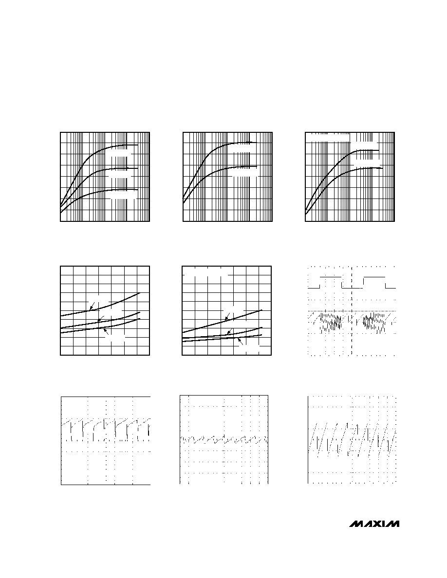
__________________________________________Typical Operating Characteristics
(Circuit of Figure 5, T
A
= +25∞C, unless otherwise noted.)
-35
-25
-30
-20
-5
0
-10
-15
5
0
10 15 20 25
5
30 35 40 45 50
LOAD-REGULATION ERROR
vs. LOAD CURRENT
(V
IN
= 5V)
MAX868-01
LOAD CURRENT (mA)
LOAD-REGULATION ERROR (mV)
V
OUT
= -7.5V
V
OUT
= -3.3V
V
OUT
= -5V
-15
-9
-12
0
-3
-6
3
0
5
10
15
20
25
LOAD-REGULATION ERROR
vs. LOAD CURRENT
(V
IN
= 3.3V)
MAX868-02
LOAD CURRENT (mA)
LOAD-REGULATION ERROR (mV)
V
OUT
= -3.3V
V
OUT
= -5V
400
410
430
440
420
480
470
460
450
500
490
-40
-20
0
20
40
60
80
100
MAXIMUM SWITCHING FREQUENCY
vs. TEMPERATURE
MAX868-03
TEMPERATURE (∞C)
MAXIMUM SWITCHING FREQUENCY (kHz)
FB = IN
V
IN
= 3.3V
V
IN
= 2V
V
IN
= 5V
MAX868
Regulated, Adjustable -2x
Inverting Charge Pump
4
_______________________________________________________________________________________
____________________________Typical Operating Characteristics (continued)
(Circuit of Figure 5, T
A
= +25∞C, unless otherwise noted.)
0
0.01
1
0.1
10
100
EFFICIENCY vs. LOAD CURRENT
(V
IN
= 5V)
10
MAX868-04
LOAD CURRENT (mA)
EFFICIENCY (%)
50
40
30
20
60
70
80
V
OUT
= -5V
V
OUT
= -7.5V
V
OUT
= -3.3V
0
0.01
1
0.1
10
100
EFFICIENCY vs. LOAD CURRENT
(V
IN
= 3.3V)
10
MAX868-05
LOAD CURRENT (mA)
EFFICIENCY (%)
50
40
30
20
60
70
80
V
OUT
= -5V
V
OUT
= -3.3V
0
0.01
1
0.1
10
100
EFFICIENCY vs. LOAD CURRENT
(V
IN
= 5V)
10
MAX868-06
LOAD CURRENT (mA)
EFFICIENCY (%)
50
40
30
20
60
70
80
CIRCUIT OF FIGURE 6
V
OUT
= -2.5V
V
OUT
= -3.3V
0
60
40
20
100
80
180
160
140
120
200
-40
-20
0
20
40
60
80
100
OPEN-LOOP OUTPUT IMPEDANCE
vs. TEMPERATURE
(FB = IN, V
OUT
= -2 x V
IN
)
MAX868-07
TEMPERATURE (∞C)
OUTPUT IMPEDANCE (
)
V
IN
= 2V
V
IN
= 3.3V
V
IN
= 5V
20
µ
s/div
20mV/div
V
IN
= 3.3V, V
OUT
= -3.3V, I
LOAD
= 5mA,
V
OUT
AC COUPLED (20mV/div), C
OUT
= 10
µ
F CERAMIC
OUTPUT VOLTAGE RIPPLE
(C
OUT
= 10
µ
F CERAMIC)
MAX868-10
0
60
40
20
100
80
180
160
140
120
200
-40
-20
0
20
40
60
80
100
OPEN-LOOP OUTPUT IMPEDANCE
vs. TEMPERATURE
(FB = IN, V
OUT
= -V
IN
)
MAX868-08
TEMPERATURE (∞C)
OUTPUT IMPEDANCE (
)
V
IN
= 2V
CIRCUIT OF FIGURE 6
V
IN
= 3.3V
V
IN
= 5V
20
µ
s/div
20mV/div
V
IN
= 3.3V, V
OUT
= -3.3V, I
LOAD
= 5mA,
V
OUT
AC COUPLED (20mV/div), C
OUT
= 10
µ
F (AVX TPS)
OUTPUT VOLTAGE RIPPLE
(C
OUT
= 10
µ
F TANTALUM)
MAX868-09
20
µ
s/div
20mV/div
V
IN
= 3.3V, V
OUT
= -3.3V, I
LOAD
= 5mA,
V
OUT
AC COUPLED (20mV/div), C
OUT
= 2.2
µ
F CERAMIC
OUTPUT VOLTAGE RIPPLE
MAX868-11
200
µ
s/div
10mA/div
20mV/div
V
IN
= 5V, V
OUT
= -5V, I
OUT
= 1mA TO 11mA STEP
LOAD-TRANSIENT RESPONSE
MAX868-12

Detailed Description
The MAX868 inverting charge pump uses pulse-
frequency-modulation (PFM) control to generate a reg-
ulated negative output voltage up to -2 x V
IN
. PFM
operation is obtained by enabling the internal 450kHz
oscillator as needed to maintain output voltage regula-
tion. This control scheme reduces supply current at
light loads and permits the use of small capacitors.
The functional diagram shown in Figure 1 indicates the
two phases of MAX868 operation: charge phase (
1)
and discharge phase (
2). In charge phase, the
switches on the left-hand side close, and the switches
on the right-hand side open. In the discharge phase,
the inverse occurs.
Figure 2 illustrates that in charge phase, both flying
capacitors are charged in parallel. The load is serviced
entirely by the charge stored in the output capacitor.
Figure 3 demonstrates the series connection of the fly-
ing capacitors in the discharge phase. The series com-
bination of the flying capacitors, when connected to the
output capacitor, transfers charge to the output in order
to maintain output voltage regulation. In normal opera-
tion, the MAX868 operates predominantly in charge
phase, switching to discharge phase only as needed to
maintain a regulated output.
MAX868
Regulated, Adjustable -2x
Inverting Charge Pump
_______________________________________________________________________________________
5
Pin Description
Active-Low Shutdown Input. Connect SHDN to GND to put the MAX868 in shutdown mode and reduce sup-
ply current to 0.1µA. Connect to IN for normal operation. OUT is actively pulled to GND in shutdown.
SHDN
9
Feedback Input. Connect FB to a resistor divider for a regulated output voltage. Connect to IN to generate
an unregulated -2 x V
IN
output voltage.
FB
10
Positive Terminal of Flying Capacitor C1
C1+
5
Negative Terminal of Flying Capacitor C2
C2-
6
Supply-Voltage Input. Input voltage range is 1.8V to 5.5V.
IN
7
Positive Terminal of Flying Capacitor C2
C2+
8
Power Ground
PGND
4
Negative Terminal of Flying Capacitor C1
C1-
3
PIN
Charge-Pump Output
OUT
2
Analog Ground
GND
1
FUNCTION
NAME
V
REF
C
OUT
OUT
C2-
C1+
C1-
FB
1
2
OSCILLATOR
C2+
IN
SHDN
Figure 1. Functional Diagram