 | –≠–ª–µ–∫—Ç—Ä–æ–Ω–Ω—ã–π –∫–æ–º–ø–æ–Ω–µ–Ω—Ç: MAX881R | –°–∫–∞—á–∞—Ç—å:  PDF PDF  ZIP ZIP |

For free samples & the latest literature: http://www.maxim-ic.com, or phone 1-800-998-8800.
For small orders, phone 408-737-7600 ext. 3468.
General Description
The MAX881R low-noise, inverting power supply is
designed for biasing GaAsFET power amplifiers in
portable wireless applications. This device is a charge-
pump inverter followed by a negative linear regulator.
The input voltage range is 2.5V to 5.5V. The output is
preset at -2.0V or can be set, using two resistors, to any
voltage from -0.5V to (-V
IN
+ 0.6V). It can deliver up to
4mA. The internal linear regulator also filters the output
to 1mVp-p ripple and noise.
Other features include a power-OK (POK) output that sig-
nals when the negative voltage is within 7.5% of its set
point. It protects the GaAsFET by not allowing power to
be applied to the GaAsFET's drain until it is properly
biased. The signal can be routed either to a microcon-
troller or directly to a switch at the GaAsFET drain. The
MAX881R is available in a space-saving 10-pin µMAX
package.
Applications
Cell Phones
PCS Phones
PHS Phones
Wireless Handsets
Wireless Modems
Two-Way Pagers
Mobile Radios
Wireless Computers
Features
o
Small µMAX Package
o
1mVp-p Output Voltage Ripple and Noise
o
Power-OK Signal to Control GaAsFET Drain
Switch
o
0.05µA Logic-Controlled Shutdown
o
1ms Guaranteed Start-Up
o
2.5V to 5.5V Input
o
-0.5V to (-V
IN
+ 0.6V) Output at up to 4mA
o
Operates with One 4.7µF and Three 0.22µF
Capacitors (no inductors needed)
MAX881R
Low-Noise Bias Supply in µMAX
with Power-OK for GaAsFET PA
________________________________________________________________
Maxim Integrated Products
1
1
2
3
4
5
10
9
8
7
6
IN
N.C.
GND
OUT
POK
N.C. = NOT INTERNALLY CONNECTED
NEGOUT
C1-
C1+
MAX881R
µ
MAX
TOP VIEW
FB
SHDN
MAX881R
IN
OUT
POK
C1+
C1-
NEGOUT
FB
GND
SHDN
CONTROLS
GaAsFET PA's
DRAIN SWITCH
OUTPUT
-2V (OR ADJ)
4mA, 1mVp-p
RIPPLE
INPUT
2.5V TO 5.5V
ON
OFF
Typical Operating Circuit
19-1372; Rev 1; 6/98
PART
MAX881REUB
-40∞C to +85∞C
TEMP. RANGE
PIN-PACKAGE
10 µMAX
EVALUATION KIT
AVAILABLE
Pin Configuration
Ordering Information

MAX881R
Low-Noise Bias Supply in µMAX
with Power-OK for GaAsFET PA
2
_______________________________________________________________________________________
ABSOLUTE MAXIMUM RATINGS
ELECTRICAL CHARACTERISTICS
(Circuit of Figure 3, V
IN
= +3.6V, FB = GND, R
L
=
, SHDN = IN,
T
A
= -40∞C to +85∞C
, unless otherwise noted. Typical values are at
T
A
= +25∞C.) (Note 2)
Stresses beyond those listed under "Absolute Maximum Ratings" may cause permanent damage to the device. These are stress ratings only, and functional
operation of the device at these or any other conditions beyond those indicated in the operational sections of the specifications is not implied. Exposure to
absolute maximum rating conditions for extended periods may affect device reliability.
IN to GND .................................................................-0.3V to +6V
SHDN to GND...........................................................-0.3V to +6V
POK to GND ...........................................................-0.3V to +12V
C1+ to GND .................................................-0.3V to (V
IN
+ 0.3V)
C1-, NEGOUT, OUT, FB to GND ....................-6V to (V
IN
+ 0.3V)
Continuous Power Dissipation (T
A
= +70∞C)
10-Pin µMAX (derate 5.6mW/∞C above +70∞C) ...........444mW
Operating Temperature Range ...........................-40∞C to +85∞C
Junction Temperature ......................................................+150∞C
Storage Temperature Range .............................-65∞C to +165∞C
Lead Temperature (soldering, 10sec) .............................+300∞C
V
IN
= 3V, R
L
= 500
, V
SHDN
= 0 to V
IN
,
POK goes low
V
IN
2.5V, I
OUT
= 0 to 4mA
Connected to IN or GND
V
IN
= 2.5V
V
IN
2.7V, I
OUT
= 0 to 4mA
V
IN
= 5.5V
V
POK
= 11V
I
OUT
= 4mA, circuit of Figure 3b
V
IN
2.7V, I
OUT
= 0 to 4mA
V
IN
2.5V, sinking 1mA
SHDN = GND
V
FB
= -0.5V
FB = OUT
CONDITIONS
ms
1
t
START
Start-Up Time
pF
10
C
IN
SHDN Input Capacitance
µA
±1
I
SHDN
SHDN Input Current
V
0.35
V
IL
SHDN Input Low Voltage
V
2.2
V
IH
SHDN Input High Voltage
µA
1
POK Off Leakage Current
mV
100
POK Output Level
% of
V
OUT
90
92.5
95
POK Threshold
kHz
80
100
120
f
OSC
Oscillator Frequency
V
-(V
IN
- 0.6)
-0.5
V
OUT
Adjustable Output Voltage
Range
V
-2.1
-2.0
-1.9
V
OUT
V
2.5
5.5
V
IN
Supply Voltage Range
Preset Output Voltage
mVp-p
1
Output Ripple
mV/mA
2
6
Output Load Regulation
µA
0.05
1
I
SHUT
Shutdown Supply Current
V
-0.515
-0.5
-0.485
V
FB
FB Voltage
nA
-10
-100
FB Input Current
µA
500
950
I
Q
Supply Current
UNITS
MIN
TYP
MAX
SYMBOL
PARAMETER
Note 1:
The output may be shorted to NEGOUT or GND if the package power dissipation is not exceeded. Typical short-circuit
current is 35mA.
-0.525
-0.475
-0.535
-0.465
V
IN
2.5V,
I
OUT
= 0 to 4mA
T
A
= +25∞C
T
A
= 0∞C to +85∞C
T
A
= -40∞C to +85∞C
Note 2:
Specifications to -40∞C are guaranteed by design, not production tested.

MAX881R
Low-Noise Bias Supply in µMAX
with Power-OK for GaAsFET PA
_______________________________________________________________________________________
3
-2.02
-1.98
-2.00
-1.94
-1.96
-1.92
1.90
-1.86
-1.88
-1.84
0
2
3
4
1
5
6
7
8
9
10
OUTPUT VOLTAGE
vs. OUTPUT CURRENT
MAX881R TOC01
OUTPUT CURRENT (mA)
OUTPUT VOLTAGE (V)
CIRCUIT OF FIGURE 3a
V
IN
= 2.5V
V
IN
3.6V
-2.02
-1.98
-2.00
-1.92
-1.94
-1.96
-1.86
-1.88
-1.90
-1.84
0
6
8
2
4
10
12
14
16
OUTPUT VOLTAGE
vs. OUTPUT CURRENT
MAX881R TOC02
OUTPUT CURRENT (mA)
OUTPUT VOLTAGE (V)
CIRCUIT OF FIGURE 3b
V
IN
= 2.5V
V
IN
3.6V
-2.03
-2.01
-2.02
-1.99
-2.00
-1.98
-1.97
-1.96
-1.95
2.0
3.0
3.5
2.5
4.0
4.5
5.0
5.5
6.0
OUTPUT VOLTAGE
vs. INPUT VOLTAGE
MAX881R TOC03
INPUT VOLTAGE (V)
OUTPUT VOLTAGE (V)
I
LOAD
= 4mA
Typical Operating Characteristics
(Circuit of Figure 3, V
IN
= 3.6V, T
A
= +25∞C, unless otherwise noted.)
0
10
5
25
20
15
40
35
30
45
2.0
3.5
4.0
2.5
3.0
4.5
5.0
5.5
6.0
MAXIMUM OUTPUT CURRENT
vs. INPUT VOLTAGE
MAX881r TOC04
INPUT VOLTAGE (V)
OUTPUT CURRENT (mA)
V
OUT
< 2mVp-p RIPPLE
CIRCUIT OF FIGURE 3b
V
OUT
< 2mVp-p RIPPLE
CIRCUIT OF FIGURE 3a
V
OUT
-1.8V
CIRCUIT OF FIGURE 3a
V
OUT
-1.8V
CIRCUIT OF FIGURE 3b
0
4
8
12
16
20
24
2.0
3.0
2.5
3.5
4.0
4.5
5.0
5.5
6.0
MAXIMUM NEGOUT CURRENT
vs. INPUT VOLTAGE
MAX881R TOC05
INPUT VOLTAGE (V)
OUTPUT CURRENT (mA)
V
NEGOUT
= 0.9 x V
NEGOUT(NO LOAD)
CIRCUIT OF FIGURE 3b
CIRCUIT OF FIGURE 3a
300
400
500
600
700
800
900
2.0
3.0
2.5
3.5
4.0
4.5
5.0
5.5
6.0
NO-LOAD SUPPLY CURRENT
vs. INPUT VOLTAGE
MAX881R TOC06
INPUT VOLTAGE (V)
SUPPLY CURRENT (
µ
A)
300
400
500
600
700
800
900
-60
-20
-40
0
20
40
60
80
100
NO-LOAD SUPPLY CURRENT
vs. TEMPERATURE
MAX881R TOC07
TEMPERATURE (∞C)
SUPPLY CURRENT (
µ
A)
V
IN
= 5.5V
V
IN
= 3.6V
V
IN
= 2.5V
100
300
200
500
400
700
600
800
2.0
3.0
3.5
2.5
4.0
4.5
5.0
5.5
6.0
START-UP TIME
vs. INPUT VOLTAGE
MAX881R TOC08
INPUT VOLTAGE (V)
START-UP TIME (
µ
s)
CIRCUIT OF FIGURE 3a
NO LOAD
SHDN TO POK DELAY
97
98
99
100
101
102
103
2.0
3.0
2.5
3.5
4.0
4.5
5.0
5.5
6.0
OSCILLATOR FREQUENCY
vs. INPUT VOLTAGE
MAX881R TOC09
INPUT VOLTAGE (V)
FREQUENCY (kHz)
T
A
= -40∞C
T
A
= +25∞C
T
A
= +85∞C

MAX881R
Low-Noise Bias Supply in µMAX
with Power-OK for GaAsFET PA
4
_______________________________________________________________________________________
Typical Operating Characteristics (continued)
(
Circuit of Figure 3, V
IN
= 3.6V, T
A
= +25∞C, unless otherwise noted.
)
100
µ
s/div
START-UP FROM SHUTDOWN
(NO LOAD)
+5V
V
OUT
POK
SHDN
MAX881R-TOC10
-2V
0
0
V
IN
0
V
IN
= 3.6V
CIRCUIT OF FIGURE 3b
5
µ
s/div
OUTPUT NOISE AND RIPPLE
(CIRCUIT OF FIGURE 3a)
V
OUT
1mV/div
AC COUPLED
MAX881R-TOC11
V
IN
= 3.6V
V
OUT
= -2V
I
OUT
= 2.5mA
10
µ
s/div
OUTPUT NOISE AND RIPPLE
(CIRCUIT OF FIGURE 3b)
V
OUT
= 0
V
IN
= 0
1mV/div
AC COUPLED
V
OUT
= -2V
V
IN
= 3.6V
1mV/div
AC COUPLED
MAX881R-TOC12
R
L
= 500
NOISE FLOOR
OUTPUT NOISE
60
-40
1
10
100
1000
OUTPUT NOISE SPECTRUM
(CIRCUIT OF FIGURE 3a)
-20
MAX881R TOC13
FREQUENCY (kHz)
NOISE (dB
µ
V)
0
20
40
50
-30
-10
10
30
V
IN
= 3.6V
V
OUT
= -2V
I
OUT
= 2.5mA
60
-40
1
10
100
1000
OUTPUT NOISE SPECTRUM
(CIRCUIT OF FIGURE 3b)
-20
MAX881R TOC14
FREQUENCY (kHz)
NOISE (dB
µ
V)
0
20
40
50
-30
-10
10
30
V
IN
= 3.6V
V
OUT
= -2V
I
OUT
= 4mA
2ms/div
LINE-TRANSIENT RESPONSE
V
IN
V
OUT
MAX881R-TOC15
10mV/
div
3.3V
2.7V
I
LOAD
= 4mA
V
OUT
= -2V
CIRCUIT OF FIGURE 3b
100
µ
s/div
LOAD-TRANSIENT RESPONSE
I
OUT
V
OUT
MAX881R-TOC16
10mV/
div
4mA
400
µ
A
V
IN
= 3.6V
V
OUT
= -2V
CIRCUIT OF FIGURE 3b
MAX881R
Low-Noise Bias Supply in µMAX
with Power-OK for GaAsFET PA
_______________________________________________________________________________________
5
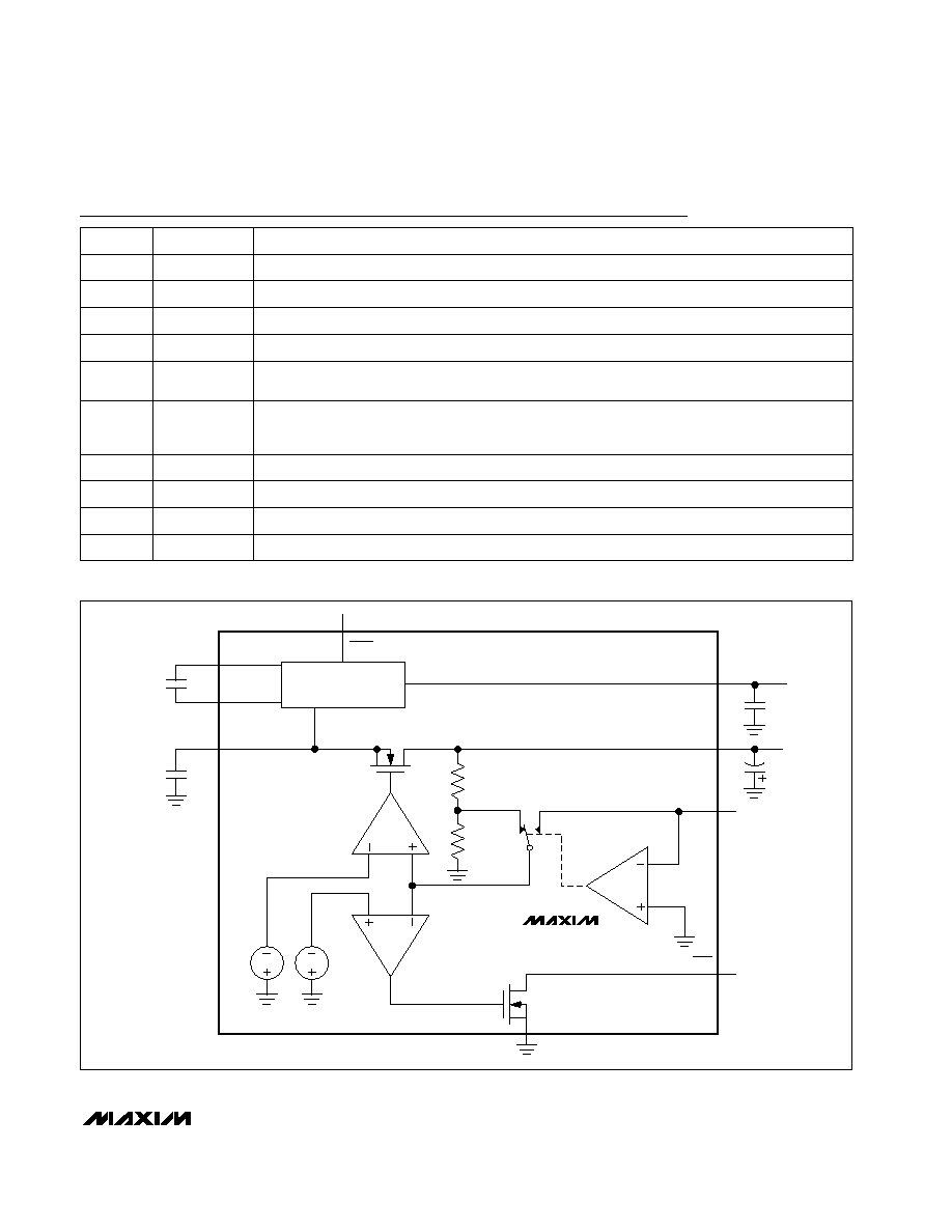
CHARGE PUMP
NEGOUT
SHDN
0.5V
0.4625V
GND
C1+
C1
C2
C4
C3
IN
OUT
FB
POK
C1-
MAX881R
Pin Description
Ground
GND
8
No Connection. Not internally connected.
N.C.
9
Positive Power-Supply Input
IN
10
Active-Low, Logic-Level Shutdown Input. Connect to IN for normal operation. Do not leave this pin
unconnected.
SHDN
5
Dual-ModeTM Feedback Input. When FB is connected to GND, the output is preset to -2V. To select
other voltages, connect FB to an external resistor-divider (Figure 4). Do not leave this pin
unconnected.
FB
6
Regulated Negative Output Voltage
OUT
7
Active-Low, Open-Drain Power-OK Output. Goes low when OUT reaches 92.5% of its set value.
POK
4
Negative Output Voltage (unregulated)
NEGOUT
3
PIN
Negative Terminal for C1
C1-
2
Positive Terminal for C1
C1+
1
FUNCTION
NAME
Figure 1. Functional Diagram
Dual-Mode is a trademark of Maxim Integrated Products.