 | –≠–ª–µ–∫—Ç—Ä–æ–Ω–Ω—ã–π –∫–æ–º–ø–æ–Ω–µ–Ω—Ç: MAX884 | –°–∫–∞—á–∞—Ç—å:  PDF PDF  ZIP ZIP |

_______________General Description
T
he MAX882/MAX883/MAX884 linear regulators maxi-
mize battery life by combining ultra-low supply currents
and low dropout voltages. They feature 200mA output
current capability at up to +125∞C junction temperature
and come in a 1.5W SOIC package. The 1.5W package
(compared to 0.47W for standard SOIC packages)
allows a wider operating range for the input voltage and
output current. The MAX882/MAX883/MAX884 use a P-
channel MOSFET pass transistor to maintain a low 11µA
(15µA max) supply current from no-load to the full
200mA output. Unlike earlier bipolar regulators, there are
no PNP base current losses that increase with output
current. And, in dropout, the MOSFET does not suffer
from excessive base currents that occur when PNP tran-
sistors go into saturation. Typical dropout voltages are
220mV at 5V and 200mA, or 320mV at 3.3V and 200mA.
The MAX882 features a 7µA standby mode that disables
the output but keeps the reference, low-battery compara-
tor, and biasing circuitry alive. The MAX883/MAX884 fea-
ture a shutdown (OFF) mode that turns off all circuitry,
reducing supply current to less than 1µA. All three
devices include a low-battery-detection comparator, fold-
back current limiting, reverse-current protection, and
thermal overload protection.
The output is preset at 3.3V for the MAX882/MAX884
and 5V for the MAX883. In addition, all devices employ
Dual ModeTM operation, allowing user-adjustable outputs
from 1.25V to 11V using external resistors. The input volt-
age supply range is 2.7V to 11.5V.
For low-dropout linear regulators with output currents up
to 500mA, refer to the MAX603/MAX604 data sheet.
________________________Applications
Pagers and Cellular Phones
3.3V and 5V Regulators
1.25V to 11V Adjustable Regulators
High-Efficiency Linear Regulators
Battery-Powered Devices
Portable Instruments
Solar-Powered Instruments
____________________________Features
o
Guaranteed 200mA Output Current at
T
J
= +125∞C, with Foldback Current Limiting
o
High-Power (1.5W) 8-Pin SO Package
o
Dual ModeTM Operation: Fixed or Adjustable
Output from 1.25V to 11V
o
Large Input Range (2.7V to 11.5V)
o
Internal 1.1
P-Channel Pass Transistor
Draws No Base Current
o
Low 220mV Dropout Voltage at 200mA
Output Current
o
11µA Typical Quiescent Current
o
1µA (max) Shutdown Mode or 7µA (typ)
Standby Mode
o
Low-Battery Detection Comparator
o
Reverse-Current Protection
o
Thermal Overload Protection
______________Ordering Information
MAX882/MAX883/MAX884
5V/3.3V or Adjustable, Low-Dropout,
Low I
Q
, 200mA Linear Regulators
________________________________________________________________
Maxim Integrated Products
1
__________________Pin Configuration
__________Typical Operating Circuit
Call toll free 1-800-998-8800 for free samples or literature.
19-0275; Rev 0; 12/94
PART
MAX882
CPA
MAX882CSA
MAX882C/D
0∞C to +70∞C
0∞C to +70∞C
0∞C to +70∞C
TEMP. RANGE
PIN-PACKAGE
8 Plastic DIP
8 SO
Dice*
Ordering Information continued at end of data sheet.
* Dice are tested at T
J
= +25∞C, DC parameters only.
** Contact factory for availability.
MAX882EPA
-40∞C to +85∞C
8 Plastic DIP
MAX882ESA
-40∞C to +85∞C
8 SO
MAX882MJA
-55∞C to +125∞C
8 CERDIP**
TM
Dual-Mode is a trademark of Maxim Integrated Products.
MAX882
MAX883
MAX884
C
IN
O.1
µ
F
C
OUT
2.2
µ
F
OUTPUT
VOLTAGE
INPUT
VOLTAGE
BATTERY
LBI
OFF (STBY)
( ) ARE FOR MAX882
IN
OUT
GND
SET
ON/OFF
LBI
OFF (STBY)
( ) ARE FOR MAX882
GND
IN
OUT
GND
SET
LBO
DIP/SO
TOP VIEW
1
2
3
4
8
7
6
5
MAX882
MAX883
MAX884

mV
MAX882/MAX883/MAX884
5V/3.3V or Adjustable, Low-Dropout,
Low I
Q
, 200mA Linear Regulators
2
_______________________________________________________________________________________
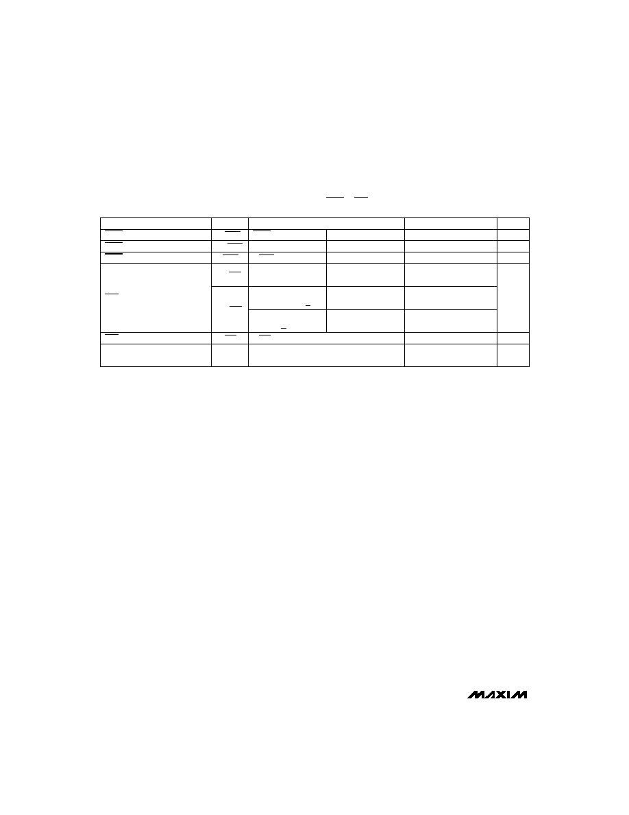
ABSOLUTE MAXIMUM RATINGS
ELECTRICAL CHARACTERISTICS
(V
IN
= 6V (MAX883) or V
IN
= 4.3V (MAX882/MAX884), C
OUT
= 2.2µF, STBY or OFF = V
IN
, SET = GND, LBI = V
IN
, T
J
= T
MIN
to T
MAX
,
unless otherwise noted. Typical values are at T
J
= +25∞C.) (Note 1)
Stresses beyond those listed under "Absolute Maximum Ratings" may cause permanent damage to the device. These are stress ratings only, and functional
operation of the device at these or any other conditions beyond those indicated in the operational sections of the specifications is not implied. Exposure to
absolute maximum rating conditions for extended periods may affect device reliability.
Supply Voltage (IN or OUT to GND).......................-0.3V to +12V
Output Short-Circuit Duration .........................................1 minute
Continuous Output Current ...............................................300mA
LBO Output Current ............................................................50mA
LBO Output Voltage and LBI,
SET, STBY, OFF Input Voltages ................-0.3V to the greater of
(IN + 0.3V) or (OUT + 0.3V)
Continuous Power Dissipation (T
J
= +70∞C)
Plastic DIP (derate 9.09mW/∞C above +70∞C) ............727mW
High-Power SO (derate 18.75mW/∞C above +70∞C) .......1.5W
CERDIP (derate 8.00mW/∞C above +70∞C) .................640mW
Operating Temperature Ranges
MAX88_C_A ........................................................0∞C to +70∞C
MAX88_E_A .....................................................-40∞C to +85∞C
MAX88_MJA ..................................................-55∞C to +125∞C
Junction Temperature .....................................................+150∞C
Storage Temperature Range .............................-65∞C to +160∞C
Lead Temperature (soldering, 10sec) .............................+300∞C
V
IN
= 11.5V
SET = OUT,
V
IN
= 6V
SET = OUT, R
L
= 1k
MAX882/MAX884
MAX883
(V
OUT
+ 0.5V) < V
IN
< 11.5V, I
OUT
= 10mA
CONDITIONS
40
I
Q
Quiescent Current
15
25
30
11
15
mV
320
640
V
DO
Dropout Voltage (Note 3)
160
320
220
440
110
220
mV
10
40
V
LNR
Line Regulation
V
3.0
11.5
V
IN
Input Voltage Range
2.9
11.5
2.7
11.5
UNITS
MIN
TYP
MAX
SYMBOL
PARAMETER
MAX88_C_A
MAX88_MJA
MAX88_E_A
I
OUT
= 10µA≠200mA,
T
J
+125∞C
I
OUT
= 10µA≠250mA,
T
J
+85∞C
I
OUT
= 100mA
I
OUT
= 100mA
MAX88_C_A/E_A
MAX88_C_A/E_A
I
OUT
= 200mA
I
OUT
= 200mA
MAX88_MJA
MAX88_MJA
µA
I
OUT
= 1mA to 150mA
MAX883C_A/E_A
I
OUT
= 1mA to 200mA
mV
30
100
V
LDR
Load Regulation
MAX883MJA
MAX882, MAX884
150
60
100
MAX882/MAX884,
4.3V
V
IN
11.5V
mV
3.15
3.30
3.45
V
OUT
Output Voltage (Note 2)
I
OUT
= 10µA≠200mA,
T
J
+85∞C
I
OUT
= 10µA≠200mA,
T
J
+70∞C
MAX883,
6.0V
V
IN
11.5V
I
OUT
= 10µA≠250mA,
T
J
+70∞C
I
OUT
= 10µA≠150mA,
T
J
+125∞C
4.75
5.00
5.25

MAX882/MAX883/MAX884
5V/3.3V or Adjustable, Low-Dropout,
Low I
Q
, 200mA Linear Regulators
_______________________________________________________________________________________
3
V
IN
= 9V, R
L
= 33
, OFF from 0V to V
IN
,
0% to 95% of V
OUT
MAX882:
V
IN
= 0V, STBY = 0V, V
OUT
= 3.0V
STBY = 0V,
V
IN
= 6V, SET = OUT
V
OUT
= 3.0V
V
OUT
< 0.8V
V
IN
= 11.5V,
SET = OUT
V
OUT
= 4.5V
STBY = 0V,
V
IN
=11.5V, SET = OUT
OFF = 0V,
R
L
= 1k
,
V
IN
= 11.5V
(MAX883/MAX884)
V
OUT
> 0.8V and V
IN
- V
OUT
> 0.7V
CONDITIONS
µs
200
T
START
Time Required to Exit OFF or
STBY Modes
I
RVL
Reverse Leakage Current
% of
V
OUT
1
µA
7
mV
6
20
V
RTH
Reverse-Current-Protection
Threshold (Note 6)
6
20
∞C
10
T
SD
Thermal Shutdown Hysteresis
∞C
160
T
SD
Thermal Shutdown Temperature
mA
430
I
LIM
Foldback Current Limit (Note 5)
10
25
30
7
15
170
µA
10
I
OUT(MIN)
Minimum Load Current
3
1
µA
40
I
Q STBY
STBY Quiescent Current
(Note 4)
0.01
1
5
µA
10
I
Q OFF
OFF Quiescent Current
UNITS
MIN
TYP
MAX
SYMBOL
PARAMETER
65
30
Dual ModeTM SET Threshold
V
SET TH
For internal feedback
150
65
SET = OUT, R
L
= 1k
1.16
1.20
1.24
mV
SET Reference Voltage
V
SET
V
SET
= 1.5V or 0V
±0.01
±50
nA
LBI Threshold Voltage
V
LBI
LBI signal falling
1.15
1.20
1.25
V
LBI Hysteresis
V
LBI
7
mV
LBI Input Leakage Current
I
LBI
V
LBI
= 1.5V
±0.01
±50
nA
LBO Output Low Voltage
V
LBOL
I
LBO SINK
= 1.2mA, V
LBI
=1V,
3V < V
IN
< 11.5V, SET = OUT
90
250
mV
LBO Output Leakage Current
I
LBO LKG
V
LBI
= V
IN
, V
LBO
= V
IN
0.01
0.1
µA
0.01
1
3
OUT Leakage Current
I
OUT LKG
V
IN
= 11.5V,
V
OUT
= 2V,
SET = OUT
10
µA
MAX882C_A/E_A
MAX882MJA
MAX882C_A/E_A
MAX882MJA
MAX88_C_A
MAX88_E_A
MAX88_MJA
MAX88_C_A
MAX88_E_A
MAX88_MJA
MAX882_A,
MAX884_A
MAX883_A
R
L
= 1k
, C
OUT
= 2.2µF
V
OSH
Startup Overshoot
For external feedback
V
SET Input Leakage Current
I
SET
MAX88_C_A
MAX88_MJA
MAX88_E_A
ELECTRICAL CHARACTERISTICS (continued)
(V
IN
= 6V (MAX883) or V
IN
= 4.3V (MAX882/MAX884), C
OUT
= 2.2µF, STBY or OFF = V
IN
, SET = GND, LBI = V
IN
, T
J
= T
MIN
to T
MAX
,
unless otherwise noted. Typical values are at T
J
= +25∞C.) (Note 1)
MAX883/MAX884:
V
IN
= 0V, OFF = 0V, V
OUT
= 3.0V
0.01
MAX882/MAX883/MAX884
5V/3.3V or Adjustable, Low-Dropout,
Low I
Q
, 200mA Linear Regulators
4
_______________________________________________________________________________________
V
STBY
= V
IN
or 0V
STBY signal falling
V
OFF
= V
IN
or 0V
In on mode, SET = OUT,
6V < V
IN
< 11.5V
In off mode
In on mode,
SET = OUT, V
IN
< 6V
10Hz to 10kHz, SET = OUT, R
L
= 1k
,
C
OUT
= 2.2µF
CONDITIONS
µV
RMS
250
e
n
Output Noise (Note 7)
nA
±0.01
±50
I
STBY
STBY Input Leakage Current
mV
7
V
STBY
V
1.15
1.20
1.25
V
STBY
STBY Threshold Voltage
STBY Hysteresis
nA
±0.01
±50
I
OFF
OFF Input Leakage Current
V
3.0
OFF Threshold Voltage
0.4
V
IL OFF
2.0
V
IH OFF
UNITS
MIN
TYP
MAX
SYMBOL
PARAMETER
Note 1:
Electrical specifications are measured by pulse testing and are guaranteed for a junction temperature (T
J
) within the
operating temperature range, unless otherwise noted. When operating C and E grade parts up to a T
J
of +125∞C, expect
performance similar to M grade specifications. For T
J
between +125∞C and +150∞C, the output voltage may drift more.
Note 2:
(V
IN
- V
OUT
) is limited to keep the product (I
OUT
x (V
IN
- V
OUT
)) from exceeding the package power dissipation limits. See
Figure 5. Therefore, the combination of high output current and high supply voltage is not tested. Output current at
T
J
= +125∞C is guaranteed by guard banding tests at T
J
= +85∞C and +70∞C.
Note 3:
Dropout Voltage is (V
IN
- V
OUT
) when V
OUT
falls to 100mV below its nominal value at V
IN
= (V
OUT
+ 2V). For example, the
MAX883 is tested by measuring the V
OUT
at V
IN
= 7V, then V
IN
is lowered until V
OUT
falls 100mV below the measured
value. The difference (V
IN
- V
OUT
) is then measured and defined as
V
DO
.
Note 4:
Since standby mode inhibits the output but keeps all biasing circuitry alive, the Standby Quiescent Current is similar to the
normal operating quiescent current.
Note 5:
Foldback Current Limit was characterized by pulse testing to remain below the maximum junction temperature (not
production tested).
Note 6:
The Reverse-Current Protection Threshold is the output/input differential voltage (V
OUT
- V
IN
) at which reverse-current
protection switchover occurs and the pass transistor is turned off. See the section
Reverse Current Protection in the
Detailed Description.
Note 7:
Noise is tested using a bandpass amplifier with two poles at 10Hz and two poles at 10kHz.
MAX882_A
MAX882_A
MAX882_A
MAX883_A,
MAX884_A
MAX883_A,
MAX884_A
MAX883_A,
MAX884_A
ELECTRICAL CHARACTERISTICS (continued)
(V
IN
= 6V (MAX883) or V
IN
= 4.3V (MAX882/MAX884), C
OUT
= 2.2µF, STBY or OFF = V
IN
, SET = GND, LBI = V
IN
, T
J
= T
MIN
to T
MAX
,
unless otherwise noted. Typical values are at T
J
= +25∞C.) (Note 1)
MAX882/MAX883/MAX884
5V/3.3V or Adjustable, Low-Dropout,
Low I
Q
, 200mA Linear Regulators
_______________________________________________________________________________________
5
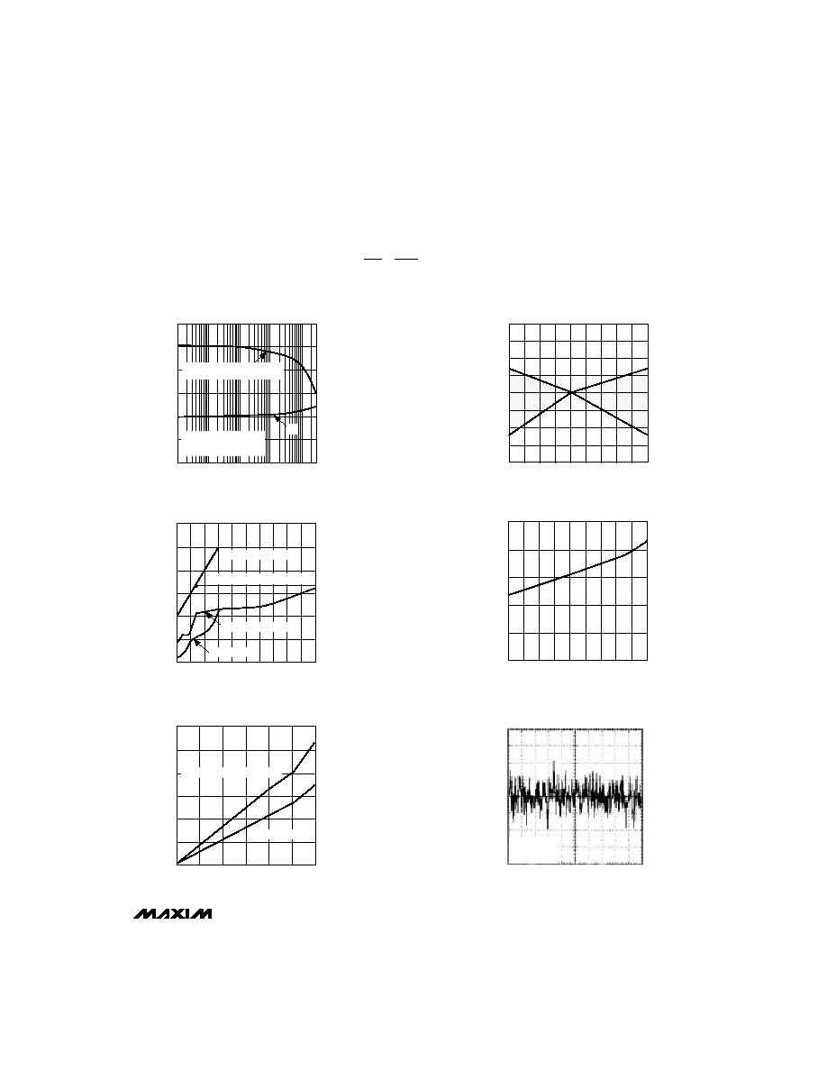
__________________________________________Typical Operating Characteristics
(V
IN
= 7V for MAX883, V
IN
= 5.3V for MAX882/MAX884, OFF or STBY = V
IN
, SET = GND, LBI = V
IN
, LBO = OPEN, C
IN
= C
OUT
= 2.2µF,
R
L
= 1k
, T
A
= +25∞C, unless otherwise noted.)
95
101
100
99
98
97
96
0.01
0.1
1
100
10
250
OUTPUT VOLTAGE AND QUIESCENT
CURRENT vs. LOAD CURRENT
MAX882/4-01
LOAD CURRENT (mA)
NORMALIZE OUTPUT VOLTAGE (%)
V
OUT
= 5V (MAX883)
V
OUT
= 3.3V (MAX882/MAX884)
OUTPUT VOLTAGE
NORMALIZED TO OUTPUT
VOLTAGE AT 1mA
0
5
10
15
20
25
30
QUIESCENT CURRENT (
µ
A)
I
Q
0
2
3
4
5
6
4
6
8
10
12
14
16
OUTPUT VOLTAGE AND QUIESCENT
CURRENT vs. SUPPLY VOLTAGE
MAX882/4-03
SUPPLY VOLTAGE (V)
OUTPUT VOLTAGE (V)
QUIESCENT CURRENT (
µ
A)
2
3
4
5
6
7
8
9
10 11 12
V
OUT
= 5V (MAX883)
V
OUT
= 3.3V (MAX882/MAX884)
I
Q
(MAX882/MAX884)
I
Q
(MAX883)
0
0.1
0.2
0.3
0.4
0.5
0.6
DROPOUT VOLTAGE
vs. LOAD CURRENT
MAX882/4-05
LOAD CURRENT (mA)
DROPPUT VOLTAGE (V)
0
50
100
150
200
250
300
V
OUT
= 3.3V (MAX882/MAX884)
V
OUT
= 5V (MAX883)
0
15
12
9
6
3
QUIESCENT CURRENT
vs. TEMPERATURE
MAX882/4-04
TEMPERATURE (∞C)
QUIESCENT CURRENT (
µ
A)
-55 -35 -15
5
25
45 65
85 105 125
10Hz to 10kHz OUTPUT NOISE
10ms/div
OUTPUT NOISE (1mV/div)
MAX883
V
OUT
= 5V
MAX882/4-06
96
97
98
99
100
101
102
103
104
OUTPUT VOLTAGE
vs. TEMPERATURE
MAX882/4-04a
TEMPERATURE (∞C)
NORMALIZED OUTPUT VOLTAGE (%)
-55 -35 -15
5
25
45 65
85 105 125