 | –≠–ª–µ–∫—Ç—Ä–æ–Ω–Ω—ã–π –∫–æ–º–ø–æ–Ω–µ–Ω—Ç: MAX8880 | –°–∫–∞—á–∞—Ç—å:  PDF PDF  ZIP ZIP |
General Description
The MAX8880/MAX8881 are ultra-low supply current,
low-dropout linear regulators, capable of delivering up
to 200mA. They are designed for battery-powered
applications where reverse battery protection and long
battery life are critical.
These regulators' low 3.5µA supply current extends
battery life in applications with long standby periods.
Unlike PNP-based designs, a 2
PMOS device main-
tains ultra-low supply current throughout the entire
operating range and in dropout. The parts are internally
protected from output short circuits, reverse battery
connection, and thermal overload. An internal power-
OK (POK) comparator indicates when the output is out
of regulation.
The MAX8880 output is adjustable from 1.25V to 5V
using an external resistor-divider. The MAX8881 pro-
vides only factory-preset output voltages of 1.8V, 2.5V,
3.3V, or 5V (see Ordering Information). Both devices
are available in miniature 6-pin SOT23 packages.
Features
o 3.5µA Supply Current at 12V
o Reverse Battery Protection
o 2.5V to 12V Input Voltage Range
o ±1.5% Output Voltage Accuracy
o 200mA max Output Current
o 2 PMOS Output Device
o Short-Circuit and Thermal Overload Protection
o POK Output for Out-of-Regulation Indicator
o Fixed 1.8V, 2.5V, 3.3V, and 5V (MAX8881)
Adjustable from 1.25V to 5V (MAX8880)
o Tiny 6-Pin SOT23 Package
MAX8880/MAX8881
12V, Ultra-Low-I
Q
, Low-Dropout
Linear Regulators with POK
________________________________________________________________ Maxim Integrated Products
1
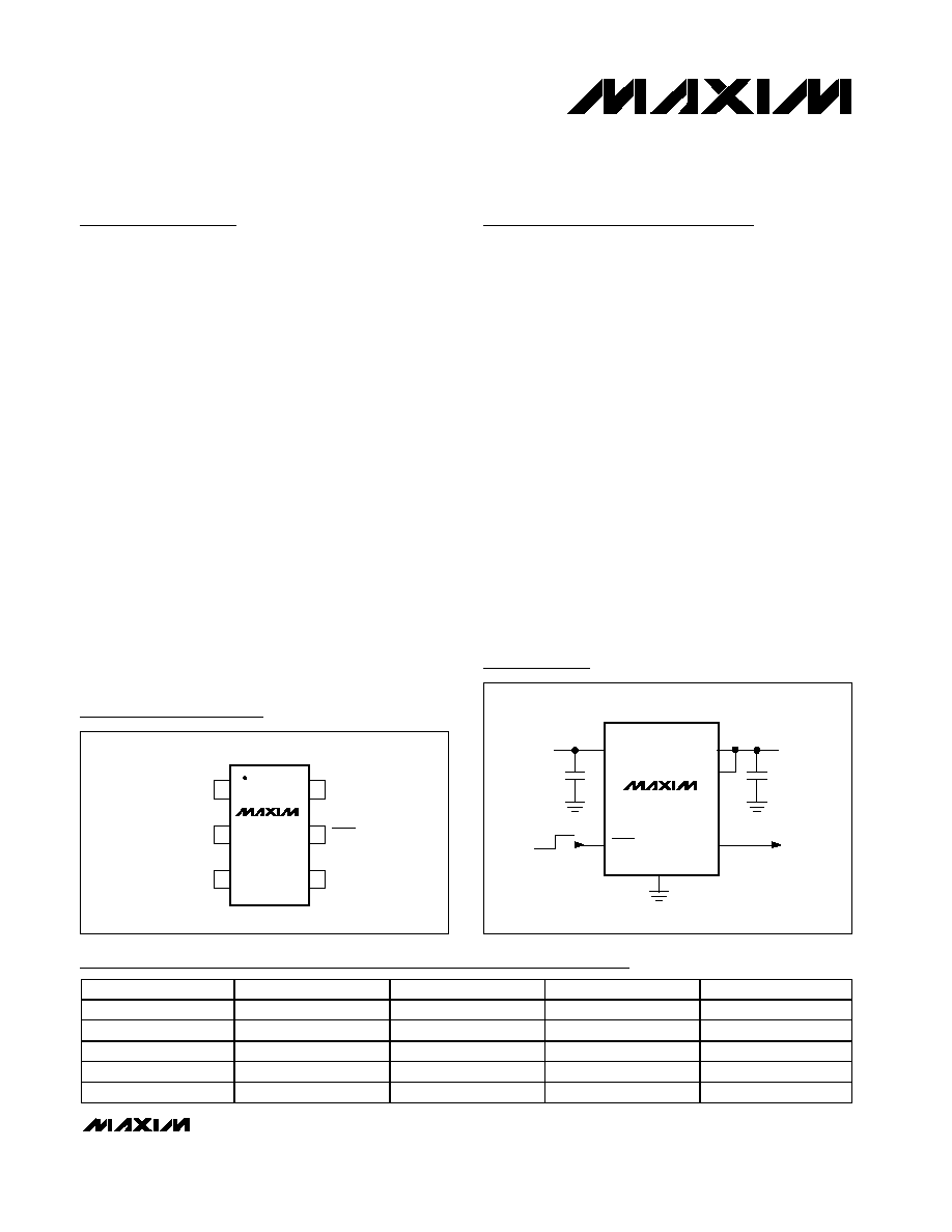
GND
FB
OUT
1
6
POK
5
SHDN
IN
MAX8880
MAX8881
SOT23-6
TOP VIEW
2
3
4
Pin Configuration
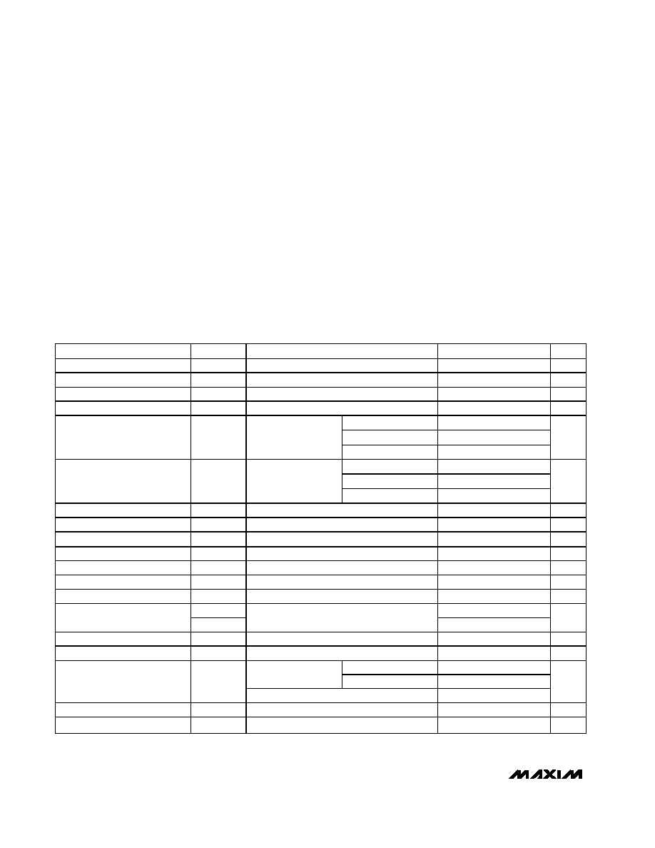
IN
OUT
FB
GND
4.7
µF
1
µF
ON
OFF
SHDN
V
IN
2.5V TO 12V
REGULATION OK
V
OUT
1.25V TO 5V
UP TO 200mA
POK
MAX8881
Typical Operating Circuit
________________________Applications
19-1679; Rev 0; 4/00
For free samples and the latest literature, visit www.maxim-ic.com or phone 1-800-998-8800.
For small orders, phone 1-800-835-8769.
Ordering Information
PART
OUTPUT
TEMP. RANGE
PIN-PACKAGE
TOP MARK
MAX8880EUT-T
Adjustable
-40
∞C to +85∞C
6 SOT23-6
AAHR
MAX8881EUT18-T
1.8V
-40
∞C to +85∞C
6 SOT23-6
AAHS
MAX8881EUT25-T
2.5V
-40
∞C to +85∞C
6 SOT23-6
AAHT
MAX8881EUT33-T
3.3V
-40
∞C to +85∞C
6 SOT23-6
AAHU
MAX8881EUT50-T
5.0V
-40
∞C to +85∞C
6 SOT23-6
AAHV
Smoke Detectors
Battery-Powered Alarms
Remote Transmitters
Smart Battery Packs
PDAs
Handy Terminals
CMOS Backup Power
Real-Time Clocks
MAX8880/MAX8881
12V, Ultra-Low-I
Q
, Low-Dropout
Linear Regulators with POK
2
_______________________________________________________________________________________
ABSOLUTE MAXIMUM RATINGS
ELECTRICAL CHARACTERISTICS
(V
IN
= V
OUT
+ 1V, SHDN = IN, C
OUT
= 4.7µF, T
A
= -40∞C to +85∞C, unless otherwise noted. Typical values are at T
A
= +25∞C.) (Note 1)
Stresses beyond those listed under "Absolute Maximum Ratings" may cause permanent damage to the device. These are stress ratings only, and functional
operation of the device at these or any other conditions beyond those indicated in the operational sections of the specifications is not implied. Exposure to
absolute maximum rating conditions for extended periods may affect device reliability.
IN to GND ................................................................-14V to +14V
SHDN to GND.............................................-0.3V to (V
IN
+ 0.3V),
-0.3V to +0.3V when V
IN
< 0V
OUT, FB to GND...............................-0.3V to +6V when V
IN
> 5.7V,
-0.3V to (V
IN
+ 0.3V) when 0V
V
IN
5.7V,
-0.3V to +0.3V when V
IN
< 0V
POK to GND ...........................................................-0.3V to +14V
OUT Continuous Current...................................................200mA
OUT Short Circuit...........................................................Indefinite
Continuous Power Dissipation (T
A
= +70
∞C)
6-Pin SOT23 (derate 8.7mW/
∞C above +70∞C)...........696mW
Operating Temperature Range ...........................-40
∞C to +85∞C
Junction Temperature ......................................................+150
∞C
Storage Temperature.........................................-65
∞C to +165∞C
Lead Temperature (soldering, 10s) .................................+300
∞C
PARAMETER
SYMBOL
CONDITIONS
MIN
TYP
MAX
UNITS
Input Voltage Range
V
IN
2.5
12
V
Supply Current
I
IN
V
IN
= 12V
3.5
10
µA
Shutdown Supply Current
I
IN(SHDN)
V
SHDN
= 0, V
IN
= 12V, V
OUT
= 0, T
A
= +25
∞C
1.5
3
µA
Input Undervoltage Lockout
V
UVLO
2.1
2.4
V
T
A
= +25
∞C
1.238
1.257
1.276
T
A
= 0
∞C to +85∞C
1.232
1.282
FB Voltage, Adjustable
Mode
V
FB
MAX8880,
I
OUT
= 20mA
T
A
= -40
∞C to +85∞C
1.219
1.295
V
T
A
= +25
∞C
-1.5
1.5
T
A
= 0
∞C to +85∞C
-2
2
OUT Voltage Accuracy
(Note 2)
MAX8881,
I
OUT
= 20mA
T
A
= -40
∞C to +85∞C
-3
3
%
OUT Voltage Range
V
OUT
MAX8880
1.25
5.5
V
OUT Line Regulation
V
IN
= V
OUT
+ 1V to 12V
0.01
0.05
%/V
OUT Load Regulation (Note 3)
I
OUT
= 10
µA to 100mA
0.006
0.015
%/mA
Current Limit (Note 3)
I
OUT
200
400
mA
Dropout Voltage (Notes 3, 4)
V
DO
I
OUT
= 50mA
100
200
mV
IN Reverse Leakage Current
I
IN(REV)
V
IN
= -12V, V
SHDN
= 0
1
mA
Foldback Current Limit
I
OUT(SC)
V
IN
= 5V, V
OUT
= 0
250
mA
V
IH
2
SHDN Input Threshold
V
IL
V
IN
= 2.5V to 12V
0.5
V
SHDN Input Bias Current
V
SHDN
= 0 to 12V, T
A
= +25
∞C
-100
100
nA
FB Input Bias Current
I
FB
FB = 1.25V, T
A
= +25
∞C, MAX8880 only
0
2
20
nA
T
A
= +25
∞C
87.5
90.5
93.5
Falling
T
A
= -40∞C to +85
∞C
86
95
POK Trip Threshold
Hysteresis
1.5
% of
V
OUT
POK Off-Current
I
POK
V
POK
= 12V, T
A
= +25
∞C
100
nA
POK Low Voltage
V
POK
I
POK
= 1mA
50
200
mV
MAX8880/MAX8881
12V, Ultra-Low-I
Q
, Low-Dropout
Linear Regulators with POK
_______________________________________________________________________________________
3
0
1.0
0.5
2.5
2.0
1.5
4.0
3.5
3.0
4.5
0
4
2
6
8
10
12
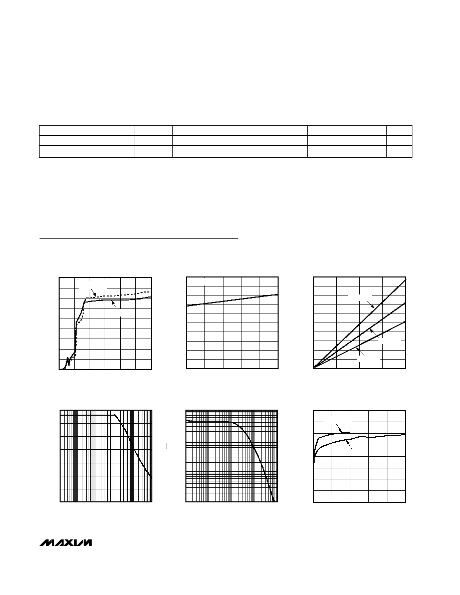
SUPPLY CURRENT
vs. INPUT VOLTAGE
MAX8880/1-01
INPUT VOLTAGE (V)
SUPPLY CURRENT (µA)
I
OUT
= 30 mA
NO LOAD
0
1.5
1.0
0.5
2.0
2.5
3.0
3.5
4.0
4.5
5.0
-40
10
-15
35
60
85
SUPPLY CURRENT
vs. TEMPERATURE
MAX8880/1-02
TEMPERATURE (∞C)
SUPPLY CURRENT (µA)
V
OUT
= 1.8V
0
150
100
50
200
250
300
350
400
450
500
0
50
100
150
200
DROPOUT VOLTAGE
vs. LOAD CURRENT
MAX8880/1-03
LOAD CURRENT (mA)
DROPOUT VOLTAGE (mV)
T
A
= +85
∞C
T
A
= +25
∞C
T
A
= -40
∞C
0
70
60
50
40
30
20
10
0.1
10
1
100
1k
10k
POWER-SUPPLY REJECTION RATIO
vs. FREQUENCY
MAX8880/1-04
FREQUENCY (Hz)
PSRR (dB)
10
100
10k
1k
100k
FREQUENCY (Hz)
10
1
0.01
0.10
MAX186-14A
OUTPUT NOISE SPECTRAL DENSITY
vs. FREQUENCY
NOISE (µV/
Hz)
0
50
100
150
200
250
300
350
400
0
20
40
60
80
100
OUTPUT NOISE
vs. LOAD CURRENT
MAX8880/1-06
LOAD CURRENT (mA)
OUTPUT NOISE (
µ
V
RMS
)
V
OUT
= 1.8V
C
OUT
= 1.0
µF
C
OUT
= 4.7
µF
Typical Operating Characteristics
(V
IN
= 5V, V
OUT
= 3.3V, I
OUT
= 30mA, C
OUT
= 4.7µF, T
A
= +25∞C, unless otherwise noted. See Figure 1.)
Note 1: All devices are 100% production tested at T
A
= +25∞C. All temperature limits are guaranteed by design.
Note 2: Output accuracy with respect to nominal preset voltages. FB = OUT.
Note 3: This specification is valid for V
IN
> 3V.
Note 4: The dropout voltage is defined as V
IN
- V
OUT
, when V
OUT
is 100mV below the value of V
OUT
for V
IN
= V
OUT
+ 1V.
ELECTRICAL CHARACTERISTICS (continued)
(V
IN
= V
OUT
+ 1V, SHDN = IN, C
OUT
= 4.7µF, T
A
= -40∞C to +85∞C, unless otherwise noted. Typical values are at T
A
= +25∞C.) (Note 1)
PARAMETER
SYMBOL
CONDITIONS
MIN
TYP
MAX
UNITS
Thermal Shutdown Threshold
T
TSD
(Hysteresis = 15
∞C)
160
∞C
OUT Noise
V
OUT(NOISE)
f = 10Hz to 100kHz, I
OUT
= 1mA
300
µV
RMS

-0.20
-0.15
-0.10
-0.05
0
0.05
0.10
0.15
0.20
-40
-15
10
35
60
85
CHANGE FROM NOMINAL OUTPUT
VOLTAGE vs. TEMPERATURE
MAX8880/1-10
TEMPERATURE (
∞C)
CHANGE FROM NOMINALOUTPUT
VOLTAGE (%)
100
0.1
0
100
200
REGION OF STABLE C
OUT
ESR
vs. OUTPUT CURRENT
1
10
MAX8880/1-11
OUTPUT CURRENT (mA)
C
OUT
ESR (
)
50
150
STABLE REGION
C
OUT
= 10µF
C
OUT
= 4.7µF
200µs/div
LINE-TRANSIENT RESPONSE
MAX8880/1-12
9.75V
9V
C
H1
= V
IN
, 500mV/div, AC COUPLED
C
H2
= V
OUT
, 20mV/div, AC COUPLED
V
OUT
= 5V, I
OUT
= 5mA
400µs/div
LOAD-TRANSIENT RESPONSE
MAX8880/1-13
32.5mA
1.25mA
C
H1
= I
OUT
, 12.5mA/div
C
H2
= V
OUT
, 100mV/div, AC COUPLED
V
OUT(NOMINAL)
= 5V, V
IN
= 9V
400µs/div
LOAD-TRANSIENT RESPONSE
NEAR DROPOUT
MAX8880/1-14
32.5mA
1.25mA
C
H1
= I
OUT
, 12.5mA/div
C
H2
= V
OUT
, 100mV/div, AC COUPLED
V
IN
= 5.2V, V
OUT(NOMINAL)
= 5V
100µs/div
TURN-ON RESPONSE
MAX8880/1-15
4V
1.8V
C
H1
= SHDN, 2V/div
C
H2
= V
OUT
, 1V/div
V
IN
= 4.0V
MAX8880/MAX8881
12V, Ultra-Low-I
Q
, Low-Dropout
Linear Regulators with POK
4
_______________________________________________________________________________________
Typical Operating Characteristics (continued)
(V
IN
= 5V, V
OUT
= 3.3V, I
OUT
= 30mA, C
OUT
= 4.7µF, T
A
= +25∞C, unless otherwise noted. See Figure 1.)
-0.6
-0.5
-0.4
-0.3
-0.2
-0.1
0
0.1
0.2
0
50
100
150
200
OUTPUT VOLTAGE ERROR
vs. LOAD CURRENT
MAX8880/1-07
LOAD CURRENT (mA)
OUTPUT VOLTAGE ERROR (%)
3.3
3.4
3.6
3.5
3.7
3.8
SUPPLY CURRENT
vs. LOAD CURRENT
MAX8880/1-08
LOAD CURRENT (mA)
SUPPLY CURRENT (
µ
A)
0
100
50
150
200
0
1.00
0.50
2.00
1.50
3.00
2.50
3.50
0
4
6
2
8
10
12
14
OUTPUT VOLTAGE
vs. INPUT VOLTAGE
MAX8880/1-09
INPUT VOLTAGE (V)
OUTPUT VOTLAGE (V)
MAX8880/MAX8881
12V, Ultra-Low-I
Q
, Low-Dropout
Linear Regulators with POK
_______________________________________________________________________________________
5
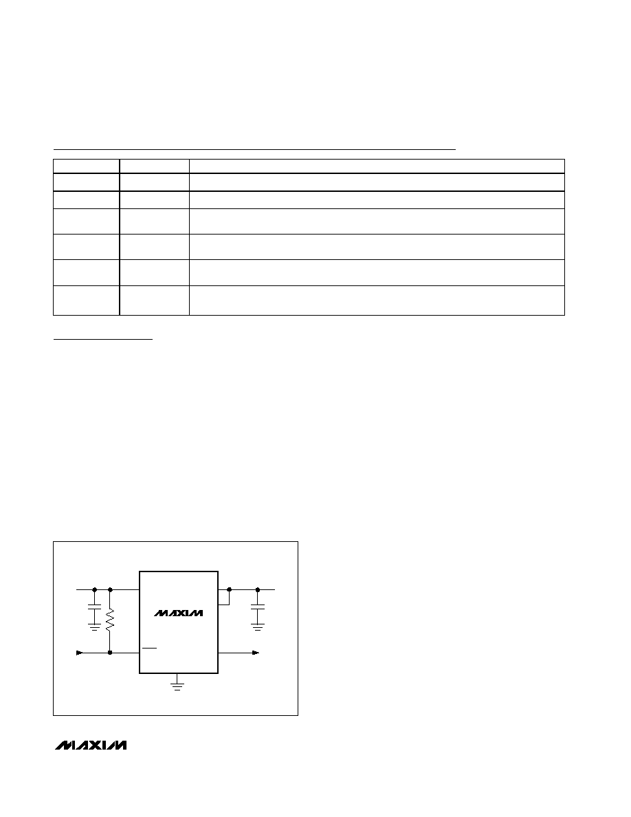
Pin Description
PIN
NAME
FUNCTION
1
IN
Input Voltage. Bypass with a 1
µF capacitor to GND.
2
GND
Ground
3
OUT
Output Voltage. Bypass with a 4.7
µF capacitor (<0.5 ESR) to GND for load currents up to
200mA. For load currents up to 40mA, 1
µF is acceptable.
4
FB
Feedback Set Point, 1.25V (MAX8880 only). Output sense, connect to OUT externally
(MAX8881EUT_ _ only).
5
SHDN
ON/OFF Control. Regulator is ON when V
SHDN
> 2V. If unused, connect to IN. If reverse
battery protection of the SHDN input is desired, connect a 100k
resistor in series with SHDN.
6
POK
POK Output, Open Drain. Low when OUT is out of regulation or in shutdown. Connect POK to
IN through a high-value resistor for a simple error indicator.
Detailed Description
The MAX8880/MAX8881 are low-dropout, low-quies-
cent current linear regulators designed primarily for
battery-powered applications (Figure 1). The MAX8880
provides an adjustable output voltage from 1.25V to 5V
using an external resistor-divider. The MAX8881 is
available in factory preset output voltages of 1.8V, 2.5V,
3.3V, and 5V. Both devices have a +1.25V reference,
error amplifier, MOSFET driver, and P-channel pass
transistor (Figure 2).
Low-Dropout Regulator
The 1.25V reference is connected to the error amplifi-
er's inverting input. The error amplifier compares this
reference with the selected feedback voltage and
amplifies the difference. The MOSFET driver reads the
error signal and applies the appropriate drive to the P-
channel pass transistor. If the feedback voltage is lower
than the reference voltage, the pass-transistor gate is
pulled lower, allowing more current to pass, increasing
the output voltage. If the feedback voltage is higher
than the reference voltage, the pass-transistor gate is
driven higher, allowing less current to pass to the out-
put. The output voltage is fed back through either an
internal resistor voltage divider by externally connect-
ing FB to OUT (MAX8881EUT_ _), or an external resis-
tor network connected to FB (MAX8880). Additional
blocks include an output current limiter, reverse battery
protection, a thermal sensor, shutdown logic, and a
POK comparator to indicate when the output is out of
regulation (Figure 2).
Internal P-Channel Pass Transistor
The MAX8880/MAX8881 feature a 2
P-channel MOS-
FET pass transistor. This provides advantages over
similar designs using PNP pass transistors, including
longer battery life. The P-channel MOSFET requires no
base drive, which reduces quiescent current consider-
ably. PNP-based regulators waste considerable current
in dropout when the pass transistor saturates. They
also use high base-drive currents under large loads.
The MAX8880/MAX8881 do not suffer from these prob-
lems and consume only 3.5µA of supply current (see
Typical Operating Characteristics).
Dropout Voltage
A regulator's minimum input-output differential (or
dropout voltage) determines the lowest usable supply
voltage. In battery-powered systems, this determines
the useful end-of-life battery voltage. Because the
MAX8880/MAX8881 use a P-channel MOSFET pass
transistor, their dropout voltage is R
DS(ON)
(2
) multi-
plied by the load current (see Electrical Characteristics).
IN
R2*
100k
OUT
FB
GND
C2
4.7
µF
C1
1
µF
SHDN
2.5V TO 12V
REGULATION OK
POK
MAX8881
V
IN
V
OUT
*OPTIONAL
Figure 1. Standard Application Circuit