 | ÐлекÑÑоннÑй компоненÑ: MAX8883 | СкаÑаÑÑ:  PDF PDF  ZIP ZIP |
Äîêóìåíòàöèÿ è îïèñàíèÿ www.docs.chipfind.ru
General Description
The MAX8882/MAX8883 dual, low-noise, low-dropout
linear regulators operate from a +2.5V to +6.5V input
and deliver up to 160mA each of continuous current.
Both versions offer low output noise and low dropout of
only 72mV at 80mA. Designed with an internal P-
channel MOSFET pass transistor, the MAX8882/
MAX8883 maintain a low 165µA supply current (both
LDOs on), independent of the load current and dropout
voltage. Other features include short-circuit protection
and thermal-shutdown protection. The MAX8882 has a
single shutdown input and provides an external refer-
ence bypass pin to improve noise performance. The
MAX8883 includes two independent logic-controlled
shutdown inputs. The MAX8882/MAX8883 are both
available in a miniature 6-pin SOT23 package.
________________________Applications
µP/DSP Core/IO Power
Cellular and PCS Telephones
PDAs and Palmtop Computers
Notebook Computers
Digital Cameras
Hand-Held Instruments
Features
o Two LDOs in Tiny SOT23
o Up to 160mA Output Current (each LDO)
o 40µV
RMS
Output Noise (MAX8882)
o 72mV Dropout at 80mA Load
o Low 165µA Operating Supply Current
o 62dB PSRR (greater than 56dB to 100kHz)
o Independent Low-Power Shutdown Controls
(MAX8883)
o Thermal-Overload and Short-Circuit Protection
o Output Current Limit
MAX8882/MAX8883
Dual, Low-Noise, Low-Dropout, 160mA Linear
Regulators in SOT23
________________________________________________________________ Maxim Integrated Products
1
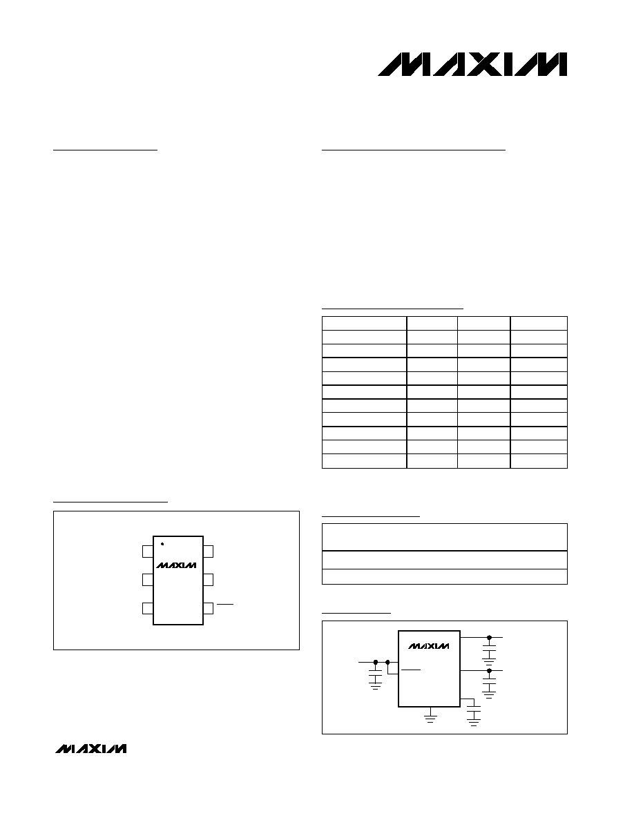
GND
SHDN
BP
1
6
OUTA
5
IN
OUTB
MAX8882
SOT23-6
TOP VIEW
2
3
4
Pin Configurations
19-1818; Rev 1; 10/01
Ordering Information
Typical Operating Circuit
PART
SH UT-
DO WN
TEMP
RANGE
PIN-
PACKAGE
MAX8882EUT_ _*
Single
-40
°C to +85°C 6 SOT23-6
MAX8883EUT_ _*
Dual
-40
°C to +85°C 6 SOT23-6
PART
V
OUTA
V
OUTB
TOP MARK
MAX8882EUTJJ
2.85
2.85
AANR
MAX8882EUTAQ
3.3
2.5
AAPW
MAX8882EUTA5
3.3
1.8
AARY
MAX8882EUTQ5
2.5
1.8
AAPX
MAX8882EUTGG
3.0
3.0
AAZT
MAX8883EUTJJ
2.85
2.85
AANS
MAX8883EUTAQ
3.3
2.5
AAPY
MAX8883EUTA5
3.3
1.8
AARZ
MAX8883EUTQ5
2.5
1.8
AAPZ
MAX8883EUTGG
3.0
3.0
AAZU
Selector Guide
2.2
µF
2.2
µF
V
IN
2.5V to 6.5V
V
OUTA
FIXED
(1.8V to 3.3V)
OUTA
OUTB
(BP)
MAX8882
MAX8883
GND
2.2
µF
V
OUTB
FIXED
(1.8V to 3.3V)
0.01
µF
( ) ARE FOR MAX8882 ONLY.
SHDN_
IN
Pin Configurations continued at end of data sheet.
***Other combinations between 1.8V and 3.3V are available in
100mV increments. Contact factory for other versions.
Minimum order quantity is 50,000 units.
For pricing, delivery, and ordering information, please contact Maxim/Dallas Direct! at
1-888-629-4642, or visit Maxim's website at www.maxim-ic.com.
*See Selector Guide
MAX8882/MAX8883
Dual, Low-Noise, Low-Dropout, 160mA Linear
Regulators in SOT23
2
_______________________________________________________________________________________
ABSOLUTE MAXIMUM RATINGS
ELECTRICAL CHARACTERISTICS
(V
IN
= +3.6V, SHDN = SHDNA = SHDNB = IN, T
A
= -40°C to +85°C, unless otherwise noted. Typical values are at T
A
= +25°C.) (Note 1)
Stresses beyond those listed under "Absolute Maximum Ratings" may cause permanent damage to the device. These are stress ratings only, and functional
operation of the device at these or any other conditions beyond those indicated in the operational sections of the specifications is not implied. Exposure to
absolute maximum rating conditions for extended periods may affect device reliability.
IN, SHDN, SHDNA, SHDNB, BP to GND...............-0.3V to +7.0V
OUTA, OUTB to GND ..................................-0.3V to (V
IN
+ 0.3V)
Output Short-Circuit Duration.....................................Continuous
Continuous Power Dissipation (T
A
= +70°C)
6-Pin SOT23 (derate 8.7mW/°C above +70°C)............695mW
Operating Temperature Range ...........................-40°C to +85°C
Junction Temperature ......................................................+150°C
Storage Temperature Range .............................-65°C to +150°C
Lead Temperature (soldering, 10s) .................................+300°C
PARAMETER
CONDITIONS
MIN
TYP
MAX
UNITS
Input Voltage
2.5
6.5
V
Undervoltage Lockout
Threshold
V
IN
_ rising, hysteresis 40mV typical
2.15
2.25
2.40
V
T
A
= +25
°C, I
OUT
_ = 1mA
-1
1
I
OUT
_ = 1mA
-2
2
Output Voltage Accuracy
I
OUT
_ = 100
µA to 160mA
-3
2
%
Maximum Output Current
Continuous
160
mA
Current Limit
160
550
mA
No Load, V
IN
= 6.5V
165
265
Ground Current
I
OUT
_ = 80mA, both LDOs
170
µA
SHDN_ = GND, T
A
= +25
°C
0.01
1
Shutdown Supply Current
SHDN_ = GND
0.1
µA
V
IH
1.6
SHDN_ Input Threshold
V
IL
0.4
V
SHDN_ = GND or IN, T
A
= +25
°C
0
100
SHDN_ Input Bias Current
SHDN_ = GND or IN
0.05
nA
I
OUT
_ = 1mA
1
I
OUT
_ = 40mA
36
Dropout Voltage
(Notes 2, 3)
I
OUT
_ = 80mA
72
144
mV
Line Regulation
V
IN
= (V
OUT
_ + 0.4V or 2.5V) to + 6.5V,
I
OUT
_ = 1mA
-0.2
0
0.2
%/V
10Hz to 100kHz, C
BP
= 0.01
µF, C
OUT
_ = 4.7
µF,
I
OUT
_ = 1mA
MAX8882
40
Output Voltage Noise
10Hz to 100kHz, C
OUT
_ = 4.7
µF, I
OUT
_ = 10mA
MAX8883
320
µV
RMS
MAX8882/MAX8883
Dual, Low-Noise, Low-Dropout, 160mA Linear
Regulators in SOT23
_______________________________________________________________________________________
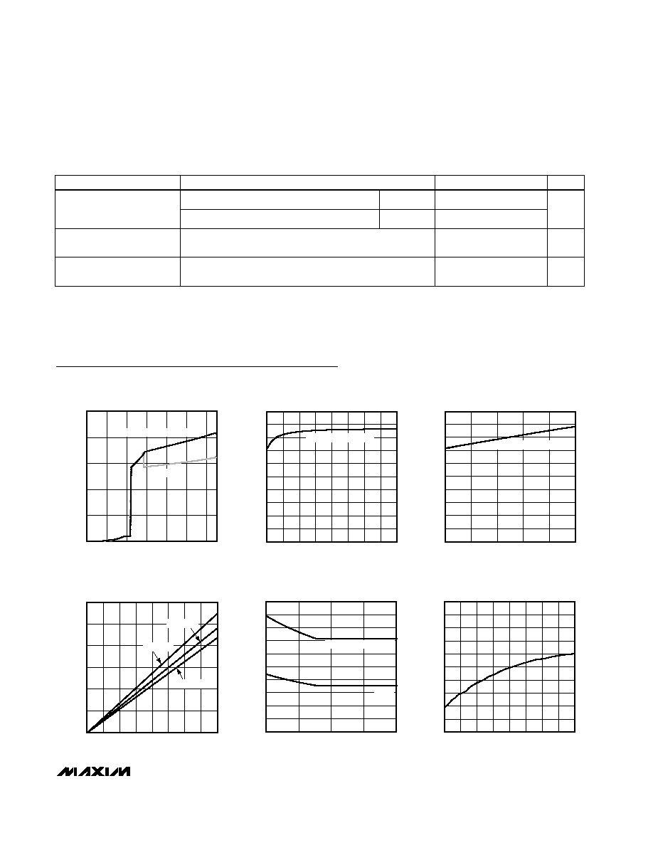
3
0
50
150
100
200
250
0
1
2
3
4
5
6
SUPPLY CURRENT
vs. SUPPLY VOLTAGE
MAX8882/3 toc01
SUPPLY VOLTAGE (V)
SUPPLY CURRENT (
µ
A)
NO LOAD
80mA LOAD, BOTH OUTPUTS
0
40
20
80
60
120
100
140
180
160
200
0
20
30
10
40
50
60
70
80
SUPPLY CURRENT
vs. LOAD CURRENT
MAX8882/3 toc02
LOAD CURRENT (mA)
SUPPLY CURRENT (
µ
A)
BOTH OUTPUTS LOADED
0
60
40
20
80
100
120
140
160
180
200
-40
10
-15
35
60
85
SUPPLY CURRENT
vs. TEMPERATURE
MAX8882/3 toc03
TEMPERATURE (
°C)
SUPPLY CURRENT (
µ
A)
80mA LOAD, BOTH OUTPUTS
0
15
30
45
60
75
90
0
20
10
30
40
50
60
70
80
DROPOUT VOLTAGE
vs. LOAD CURRENT
MAX8882/3 toc04
LOAD CURRENT (mA)
DROPOUT VOLTAGE (mV)
T
A
= +25
°C
T
A
= +85
°C
T
A
= -40
°C
0
60
40
20
80
100
120
140
160
180
200
2.5
2.7
2.9
3.1
3.3
DROPOUT vs. V
OUT
MAX8882/83 toc05
V
OUT
(V)
DROPOUT (mV)
GUARANTEED MAXIMUM
MEAN
-1.0
-0.6
-0.8
-0.2
-0.4
0.2
0
0.4
0.8
0.6
1.0
-40
-10
5
-25
20
35
50
65
80
OUTPUT VOLTAGE ACCURACY
vs. TEMPERATURE
MAX8882/83 toc06
TEMPERATURE (
°C)
OUTPUT VOLTAGE (%)
Typical Operating Characteristics
(V
OUT
_ = 2.85V, I
OUT
_ = 80mA, V
IN
= +3.6V, C
OUT
_ = 2.2µF, C
BP
= 0.01µF, and C
IN
= 2.2µF, unless otherwise noted.)
Note 1: All units are 100% production tested at T
A
= +25°C. Limits over the operating temperature range are
guaranteed by design.
Note 2: The dropout voltage is defined as V
IN
- V
OUT
when V
IN
= V
OUT
(NOM). Specification only applies when V
OUT
2.5V.
Note 3: See the Typical Operating Characteristics for guaranteed specifications at voltages other than 3.3V.
PARAMETER
CONDITIONS
MIN
TYP
MAX
UNITS
100Hz, C
BP
= 0.01
µF, C
OUT
_ = 4.7
µF
MAX8882
62
Output Voltage AC PSRR
100Hz, C
OUT
_ = 4.7
µF
MAX8883
60
dB
Thermal Shutdown
Temperature
160
°C
Thermal Shutdown
Hysteresis
10
°C
ELECTRICAL CHARACTERISTICS (continued)
(V
IN
= +3.6V, SHDN = SHDNA = SHDNB = IN, T
A
= -40°C to +85°C, unless otherwise noted. Typical values are at T
A
= +25°C.) (Note 1)
MAX8882/MAX8883
Dual, Low-Noise, Low-Dropout, 160mA Linear
Regulators in SOT23
4
_______________________________________________________________________________________
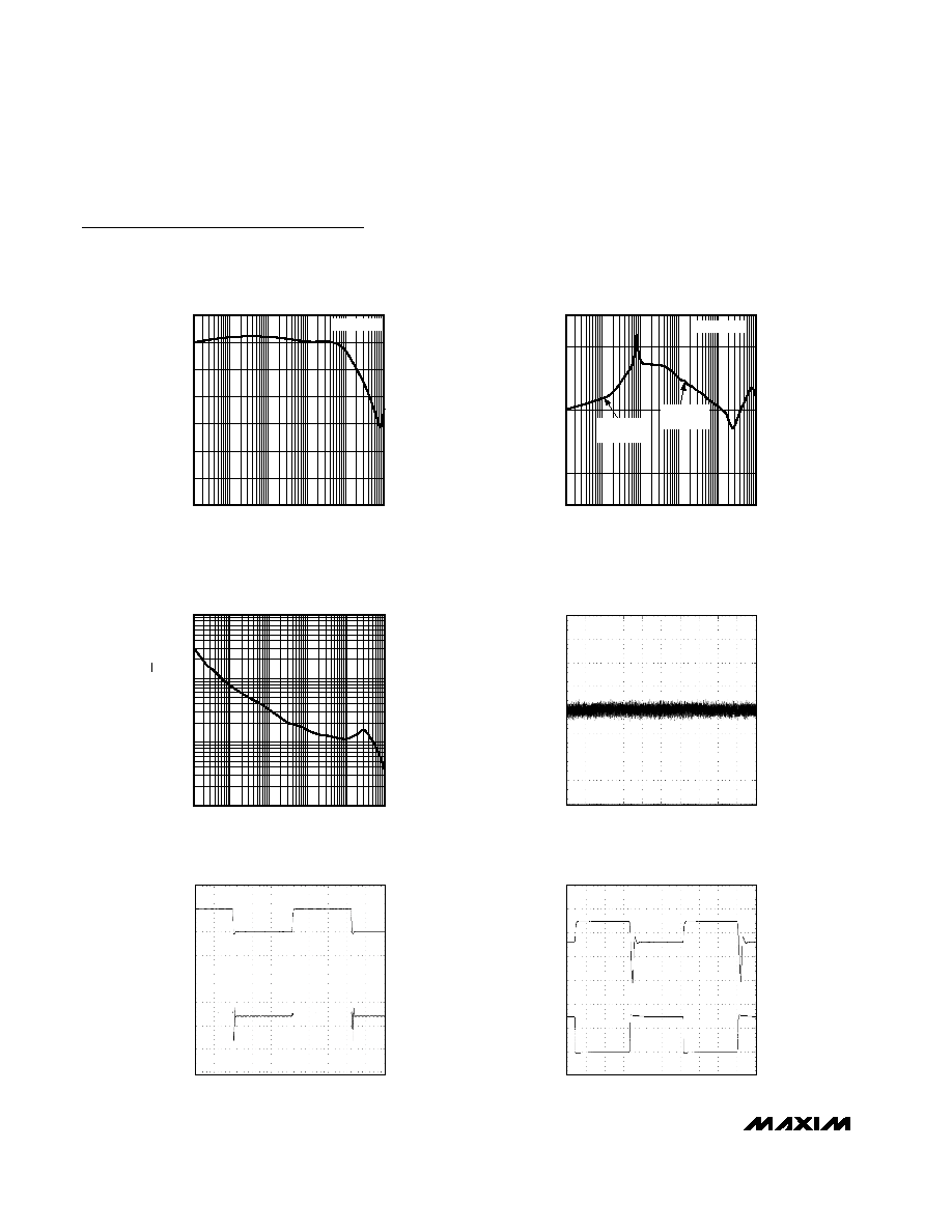
Typical Operating Characteristics (continued)
(V
OUT
_ = 2.85V, I
OUT
_ = 80mA, V
IN
= +3.6V, C
OUT
_ = 2.2µF, C
BP
= 0.01µF, and C
IN
= 2.2µF, unless otherwise noted.)
MAX8882 OUTPUT NOISE
(10Hz to 100kHz)
MAX8882/3 toc10
1ms/div
500
µV/div
(AC-COUPLED)
V
OUT
_
LINE TRANSIENT
MAX8882/3 toc11
50
µs/div
V
IN
V
OUT
_
4.5V
3.5V
1V/div
20mV/div
(AC-COUPLED)
LOAD TRANSIENT
(V
IN
= 3.35V, I
LOAD
= 0 TO 80mA)
MAX8882/3 toc12
10
µs/div
V
OUT
_
I
LOAD
0
20mV/div
(AC-COUPLED)
50mA/div
0
20
10
40
30
60
50
70
0.01
1
0.1
10
100
1000
PSRR vs. FREQUENCY
MAX8882/3 toc07
FREQUENCY (kHz)
PSRR (dB)
100
LOAD
0.01
0.1
1
1000
CHANNEL-TO-CHANNEL ISOLATION
vs. FREQUENCY
MAX8882/3 toc08
FREQUENCY (kHz)
CHANNEL-TO-CHANNEL ISOLATION (dB)
120
0
20
40
60
80
100
10
100
100
LOAD
THERMAL
COUPLING
CAPACITVE
COUPLING
10000
10
0.01
10
1000
OUTPUT NOISE SPECTRAL DENSITY
vs. FREQUENCY
100
1000
MAX8882/3 toc09
NOISE DENSITY (nV/
Hz)
0.1
1
100
MAX8882/MAX8883
Dual, Low-Noise, Low-Dropout, 160mA Linear
Regulators in SOT23
_______________________________________________________________________________________
5
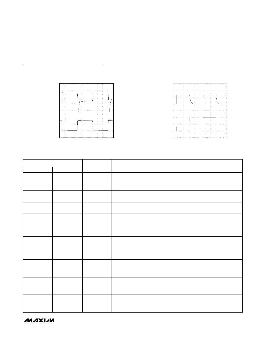
Pin Description
LOAD TRANSIENT NEAR DROPOUT
MAX8882/3 toc13
10
µs/div
20mV/div
0
50
µA/div
V
OUT
I
LOAD
V
IN
= V
OUT
+ 0.1V
SHUTDOWN RESPONSE
MAX8882/3 toc14
1ms/div
20V/div
OUTPUT
VOLTAGE
SHUTDOWN
VOLTAGE
0
0
1V/div
R
LOAD
= 100
PIN
MAX8882
MAX8883
NAME
FUNCTION
1
1
OUTB
Regulator B Output. Sources up to 160mA continuous current. Bypass with a
2.2
µF (<0.5 typ ESR) capacitor to GND (see the Capacitor Selection and
Regulator Stability section).
2
2
GND
Ground. This pin also functions as a heatsink. Solder to a large pad or the
circuit-board ground plane to maximize thermal dissipation.
3
--
BP
Reference Noise Bypass. Bypass with a low-leakage 0.01
µF ceramic
capacitor for reduced noise at both outputs.
--
3
SHDNA
Shutdown A Input. A logic low shuts down regulator A. If SHDNA and
SHDNB are both low, both regulators and the reference turn off, and supply
current is reduced to 10nA. If either SHDNA or SHDNB is a logic high, the
reference is on. Connect to IN for normal operation.
--
4
SHDNB
Shutdown B Input. A logic low shuts down regulator B. If SHDNA and
SHDNB are both low, both regulators and the reference turn off, and supply
current is reduced to 10nA. If either SHDNA or SHDNB is a logic high, the
reference is on. Connect to IN for normal operation.
4
--
SHDN
Shutdown Input. A logic low shuts down both regulators and the reference,
reducing the entire supply current to 10nA. Connect to IN for normal
operation.
5
5
IN
Regulator Input. Supply voltage can range from +2.5V to +6.5V. This input
also supplies the on-chip reference. Bypass with 2.2
µF to GND (see the
Capacitor Selection and Regulator Stability section).
6
6
OUTA
Regulator A Output. Sources up to 160mA continuous current. Bypass with
a 2.2
µF (<0.5 typ ESR) capacitor to GND (see the Capacitor Selection and
Regulator Stability section).
Typical Operating Characteristics (continued)
(V
OUT
_ = 2.85V, I
OUT
_ = 80mA, V
IN
= +3.6V, C
OUT
_ = 2.2µF, C
BP
= 0.01µF, and C
IN
= 2.2µF, unless otherwise noted.)