 | –≠–ª–µ–∫—Ç—Ä–æ–Ω–Ω—ã–π –∫–æ–º–ø–æ–Ω–µ–Ω—Ç: MAX8885 | –°–∫–∞—á–∞—Ç—å:  PDF PDF  ZIP ZIP |
For free samples & the latest literature: http://www.maxim-ic.com, or phone 1-800-998-8800.
For small orders, phone 1-800-835-8769.
General Description
The MAX8885 low-dropout (LDO) linear regulator operates
from a +2.5V to +6.5V input voltage range and delivers up
to 150mA. It uses a P-channel MOSFET pass transistor to
allow a low 85µA supply current--which is independent of
the load--as well as LDO voltage. The MAX8885 is opti-
mized to operate with low-cost, high-ESR output capaci-
tors such as small case-size tantalum capacitors. It is ideal
for cost-sensitive portable equipment such as PCS and
cellular phones. For a pin-compatible, functionally equiva-
lent device for use with a low-ESR, ceramic output capaci-
tor, refer to the MAX8875 data sheet.
The MAX8885 features a power-OK output that indicates
when the output is out of regulation, and is available in
preset output voltage versions of 5.0V, 3.3V, 3.0V, 2.7V,
and 2.5V. Other features include 1µA (max) shutdown cur-
rent, short-circuit protection, thermal shutdown protection,
and reverse-battery protection. The MAX8885 is available
in a miniature 5-pin SOT23 package.
Applications
PCS Phones
Modems
Cellular Phones
Hand-Held Instruments
Cordless Phones
Palmtop Computers
PCMCIA Cards
Electronic Planners
Features
o Optimized for Low-Cost Tantalum Capacitors
o Pin Compatible with MIC5206
o Undervoltage Power-OK Output
o Preset Output Voltages (±1% accuracy)
o Guaranteed 150mA Output Current
o 85µA No-Load Supply Current
o Low 110mV Dropout at 100mA Load (165mV at
150mA load)
o Thermal-Overload and Short-Circuit Protection
o Reverse-Battery Protection
o 60dB PSRR at 100Hz
o 1µA max Shutdown Current
MAX8885
150mA, Low-Dropout Linear Regulator
with Power-OK Output
________________________________________________________________ Maxim Integrated Products
1
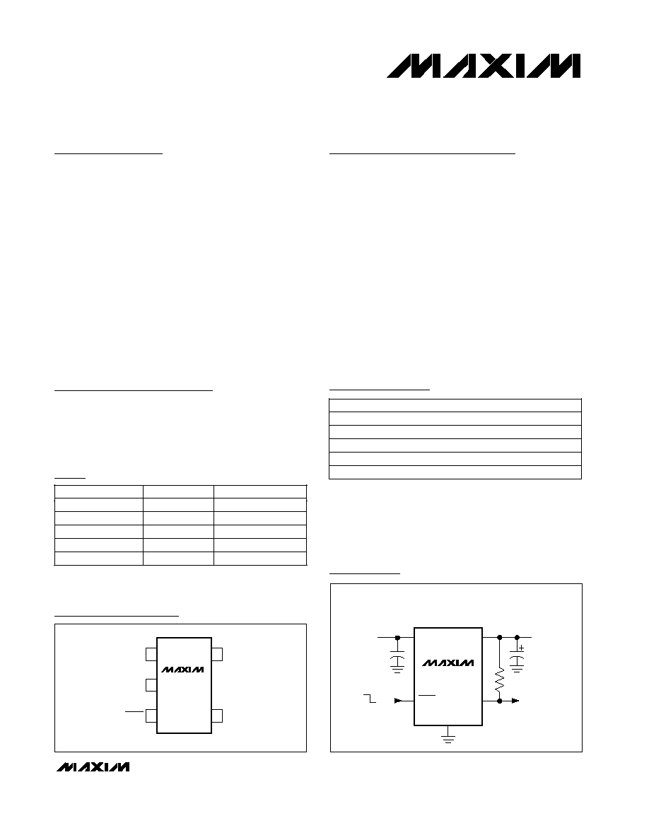
GND
POK
SHDN
1
5
OUT
IN
MAX8885
SOT23-5
TOP VIEW
2
3
4
MAX8885
INPUT
+2.5V TO +6.5V
IN
OUT
SHDN
GND
OUTPUT
PRESET
2.5V TO 5.0V
150mA
POK
C
OUT
4.7
µF
100k
C
IN
1
µF
TO
µC
OFF
ON
Typical Operating Circuit
19-1576; Rev 0; 10/99
PART
MAX8885EUK25
MAX8885EUK27
MAX8885EUK30
-40∞C to +85∞C
-40∞C to +85∞C
-40∞C to +85∞C
TEMP. RANGE
PIN-PACKAGE
5 SOT23-5
5 SOT23-5
5 SOT23-5
Note: See Output Voltage Selector Guide for more information.
Pin Configuration
Ordering Information
MAX8885EUK33
MAX8885EUK50
-40∞C to +85∞C
-40∞C to +85∞C
5 SOT23-5
5 SOT23-5
Output Voltage Selector Guide
Note: Other output voltages between 2.5V and 5.0V are avail-
able in 100mV increments--contact factory for information.
Minimum order quantity is 25,000 units.
PART
MAX8885EUK25
MAX8885EUK27
MAX8885EUK30
MAX8885EUK33
MAX8885EUK50
V
OUT
(V)
2.5
2.7
3.0
3.3
5.0
TOP MARK
ADLE
ADLF
ADLG
ADLH
ADLJ
MAX8885
150mA, Low-Dropout Linear Regulator
with Power-OK Output
2
_______________________________________________________________________________________
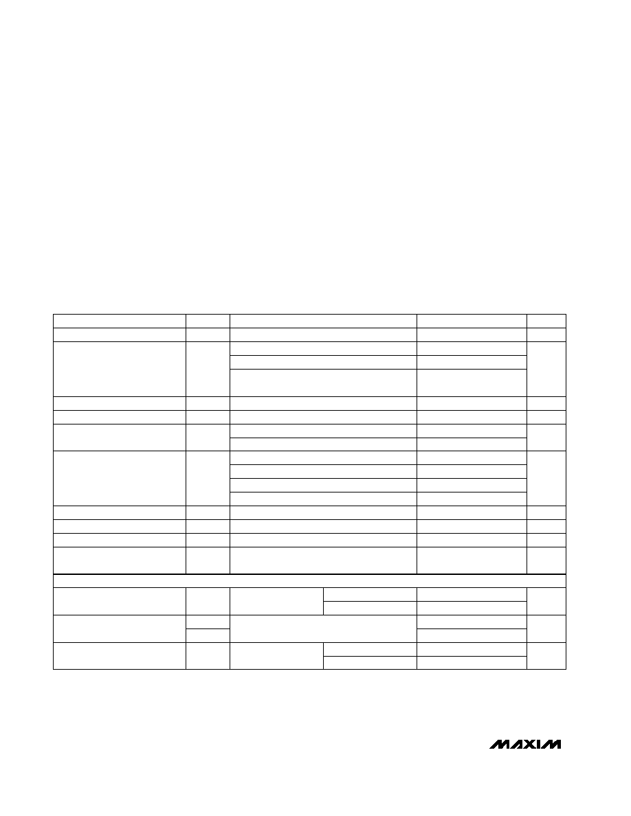
ABSOLUTE MAXIMUM RATINGS
ELECTRICAL CHARACTERISTICS
(V
IN
= V
OUT(NOMINAL)
+ 1V, SHDN = I
N
, T
A
= -40∞C to +85∞C, unless otherwise noted. Typical values are at T
A
= +25∞C.) (Note 1)
Stresses beyond those listed under "Absolute Maximum Ratings" may cause permanent damage to the device. These are stress ratings only, and functional
operation of the device at these or any other conditions beyond those indicated in the operational sections of the specifications is not implied. Exposure to
absolute maximum rating conditions for extended periods may affect device reliability.
IN, SHDN, POK to GND...............................................-7V to +7V
SHDN to IN ...............................................................-7V to +0.3V
OUT to GND ................................................-0.3V to (V
IN
+ 0.3V)
Output Short-Circuit Duration ........................................Indefinite
Continuous Power Dissipation (T
A
= +70∞C)
5-Pin SOT23 (derate 7.1mW/∞C above +70∞C)..........571mW
Operating Temperature Range ...........................-40∞C to +85∞C
Junction Temperature ......................................................+150∞C
JA
..................................................................................140∞C/W
Storage Temperature Range .............................-65∞C to +150∞C
Lead Temperature (soldering, 10s) .................................+300∞C
T
A
= +25∞C
T
A
= -40∞C to +85∞C, I
OUT
= 100µA
V
IN
= 2.5V to 5.5V
T
A
= +25∞C, I
OUT
= 100µA
SHDN = GND
f = 100Hz
I
OUT
= 100mA
I
OUT
= 50mA
C
OUT
= 10µF, f = 10Hz to 100kHz
I
OUT
= 100µA to 120mA, C
OUT
= 4.7µF
I
OUT
= 100µA
I
OUT
= 150mA
T
A
= -40∞C to +85∞C,
I
OUT
= 100µA to 120mA
V
IN
= (V
OUT
+ 0.1V) to 6.5V, I
OUT
= 1mA
I
OUT
= 100µA
I
OUT
= 150mA
CONDITIONS
0.05
nA
0
100
I
SHDN
SHDN Input Bias Current
0.4
V
IL
V
2.0
V
IH
SHDN Input Threshold
0.02
µA
0.005
1
I
OFF
Shutdown Supply Current
dB
60
PSRR
Output Voltage AC Power-
Supply Rejection Ratio
µV
RMS
170
Output Voltage Noise
%/mA
0.01
V
LDR
Load Regulation
%/V
-0.15
0
0.15
V
LNR
Line Regulation
165
%
-2
2
-1
1
V
2.5
6.5
V
IN
Input Voltage
Output Voltage Accuracy
110
220
mV
50
0.1
V
IN
-
V
OUT
Dropout Voltage (Note 2)
100
-3
2
mA
150
I
OUT
Maximum Output Current
mA
160
390
I
LIM
Current Limit
µA
85
180
I
Q
Ground Pin Current
UNITS
MIN
TYP
MAX
SYMBOL
PARAMETER
T
A
= +25∞C
T
A
= +85∞C
V
SHDN
= 5.5V or GND
T
A
= +85∞C
SHUTDOWN
MAX8885
150mA, Low-Dropout Linear Regulator
with Power-OK Output
_______________________________________________________________________________________
3
Note 1: Limits are 100% production tested at T
A
= +25∞C. Limits over the operating temperature range are guaranteed through cor-
relation using Statistical Quality Control (SQC) methods.
Note 2: Dropout voltage is defined as V
IN
- V
OUT
, when V
OUT
is 100mV below the value of V
OUT
for V
IN
= V
OUT
+ 0.5V.
ELECTRICAL CHARACTERISTICS (continued)
(V
IN
= V
OUT(NOMINAL)
+ 1V, SHDN = I
N
, T
A
= -40∞C to +85∞C, unless otherwise noted. Typical values are at T
A
= +25∞C.) (Note 1)
CONDITIONS
UNITS
MIN
TYP
MAX
SYMBOL
PARAMETER
I
SINK
= 1mA
Hysteresis, I
OUT
= 0
In dropout, V
OUT
falling
(1 - V
OUT
/ V
OUT(NOMINAL)
)100, V
OUT
falling,
I
OUT
= 0
V
0.4
V
OL
POK Output Voltage Low
1
-5.3
%
-3
-5
-8
V
POK
Power-OK Voltage Threshold
0
V
POK
6.5V, V
OUT
in regulation
∞C
20
T
SHDN
Thermal Shutdown Hysteresis
∞C
170
T
SHDN
Thermal Shutdown Temperature
µA
1
POK Output Leakage Current
Typical Operating Characteristics
(MAX8885EUK30, V
IN
= +3.6V, C
IN
= 1µF, C
OUT
= 4.7µF, SHDN = IN, T
A
= +25∞C, unless otherwise noted.)
0
40
20
80
60
100
120
0
2
3
1
4
5
6
GROUND PIN CURRENT
vs. INPUT VOLTAGE
MAX8885toc01
INPUT VOLTAGE (V)
GROUND PIN CURRENT (
µ
A)
I
OUT
= 0
I
OUT
= 150mA
85
100
95
90
105
110
115
0
60
45
15 30
75 90 105 120 135 150
GROUND PIN CURRENT vs.
OUTPUT LOAD
MAX8885toc02
OUTPUT LOAD (mA)
GROUND PIN CURRENT (
µ
A)
V
IN
= 3.5V
V
IN
= 5.0V
85
100
105
95
90
110
115
120
0
60
45
15 30
75 90 105 120 135 150
GROUND PIN CURRENT vs.
OUTPUT LOAD
MAX8885toc03
OUTPUT LOAD (mA)
GROUND PIN CURRENT (
µ
A)
V
IN
= V
OUT(NOMINAL)
+ 0.5V
V
OUT
= 5.0V
MAX8885EUK50
V
OUT
= 3.0V
MAX8885EUK30
POWER-OK OUTPUT
THERMAL PROTECTION
MAX8885
150mA, Low-Dropout Linear Regulator
with Power-OK Output
4
_______________________________________________________________________________________
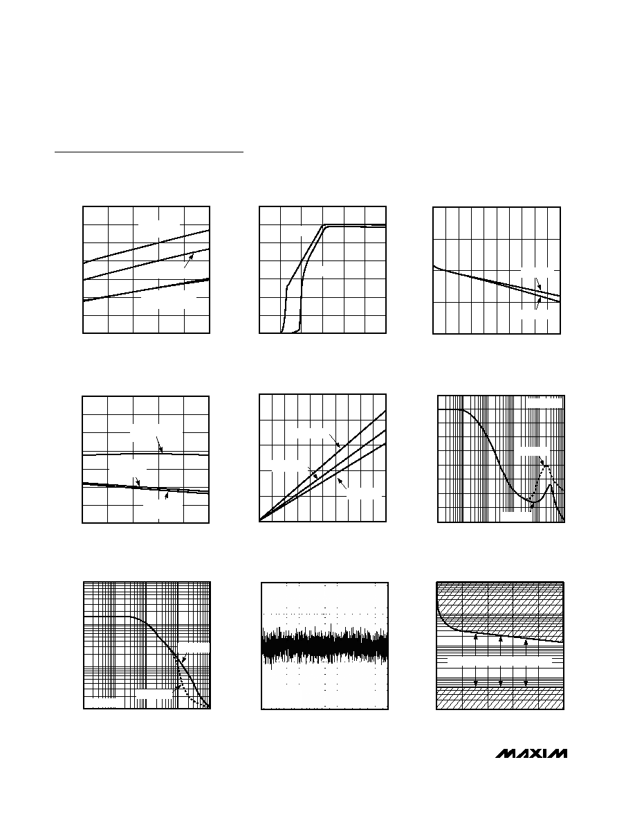
Typical Operating Characteristics (continued)
(MAX8885EUK30, V
IN
= +3.6V, C
IN
= 1µF, C
OUT
= 4.7µF, SHDN = IN, T
A
= +25∞C, unless otherwise noted.)
60
80
70
100
90
120
110
130
-40
10
-15
35
60
85
GROUND PIN CURRENT
vs. TEMPERATURE
MAX8885toc04
TEMPERATURE (∞C)
GROUND PIN CURRENT (
µ
A)
V
IN
= 5.0V
I
OUT
= 150mA
V
IN
= 3.6V
I
OUT
= 150mA
V
IN
= 3.6V OR 5.0V
I
OUT
= 0
0
1.0
0.5
2.0
1.5
3.0
2.5
3.5
0
2
3
1
4
5
6
OUTPUT VOLTAGE vs.
INPUT VOLTAGE
MAX8885toc05
INPUT VOLTAGE (V)
OUTPUT VOLTAGE (V)
I
OUT
= 0
I
OUT
= 150mA
0
60
45
15 30
75 90 105 120 135 150
2.90
2.95
3.00
3.05
3.10
OUTPUT VOLTAGE vs. OUTPUT LOAD
MAX8885toc06
OUTPUT LOAD (mA)
OUTPUT VOLTAGE (V)
V
IN
= 3.6V
V
IN
= 5.0V
60
80
110
130
OUTPUT VOLTAGE vs. TEMPERATURE
OUTPUT VOLTAGE (V)
MAX8885toc07
TEMPERATURE (∞C)
120
100
90
70
-40
-15
10
35
60
85
V
IN
= 5.0V
I
OUT
= 150mA
V
IN
= 3.6V OR 5.0V
I
OUT
= 0
V
IN
= 3.6V
I
OUT
= 150mA
0
60
45
15 30
75 90 105 120 135 150
0
150
100
50
200
250
DROPOUT VOLTAGE vs.
OUTPUT LOAD
MAX8885toc08
OUTPUT LOAD (mA)
DROPOUT VOLTAGE (mV)
T
A
= +25∞C
T
A
= -40∞C
T
A
= +85∞C
0.01
0.1
1
10
100
1000
POWER-SUPPLY REJECTION RATIO
vs. FREQUENCY
40
45
30
35
20
25
50
55
60
65
MAX8885toc09
FREQUENCY (kHz)
PSRR (dB)
R
OUT
= 60
C
OUT
= 10
µF
C
OUT
= 1
µF
10
0.01
0.1
10
100
1000
OUTPUT NOISE SPECTRAL DENSITY
vs. FREQUENCY
0.1
1
MAX8885toc10
FREQUENCY (kHz)
OUTPUT NOISE SPECTRAL DENSITY (
µ
V/
Hz
)
1
I
OUT
= 50mA
C
OUT
= 10
µF
C
OUT
= 1
µF
10ms/div
OUTPUT NOISE (10Hz TO 100kHz)
V
OUT
500
µV/div
MAX8885toc11
C
OUT
= 10
µF
I
LOAD
= 50mA
1
60
30
120
90
150
REGION OF STABLE C
OUT
ESR vs.
LOAD CURRENT
MAX8885toc12
LOAD CURRENT (mA)
C
OUT
ESR (
)
1000
0.1
1
10
100
STABLE REGION: C
OUT
= 4.7
µF TO 10µF
150mA, Low-Dropout Linear Regulator
with Power-OK Output
_______________________________________________________________________________________
5
100
µs/div
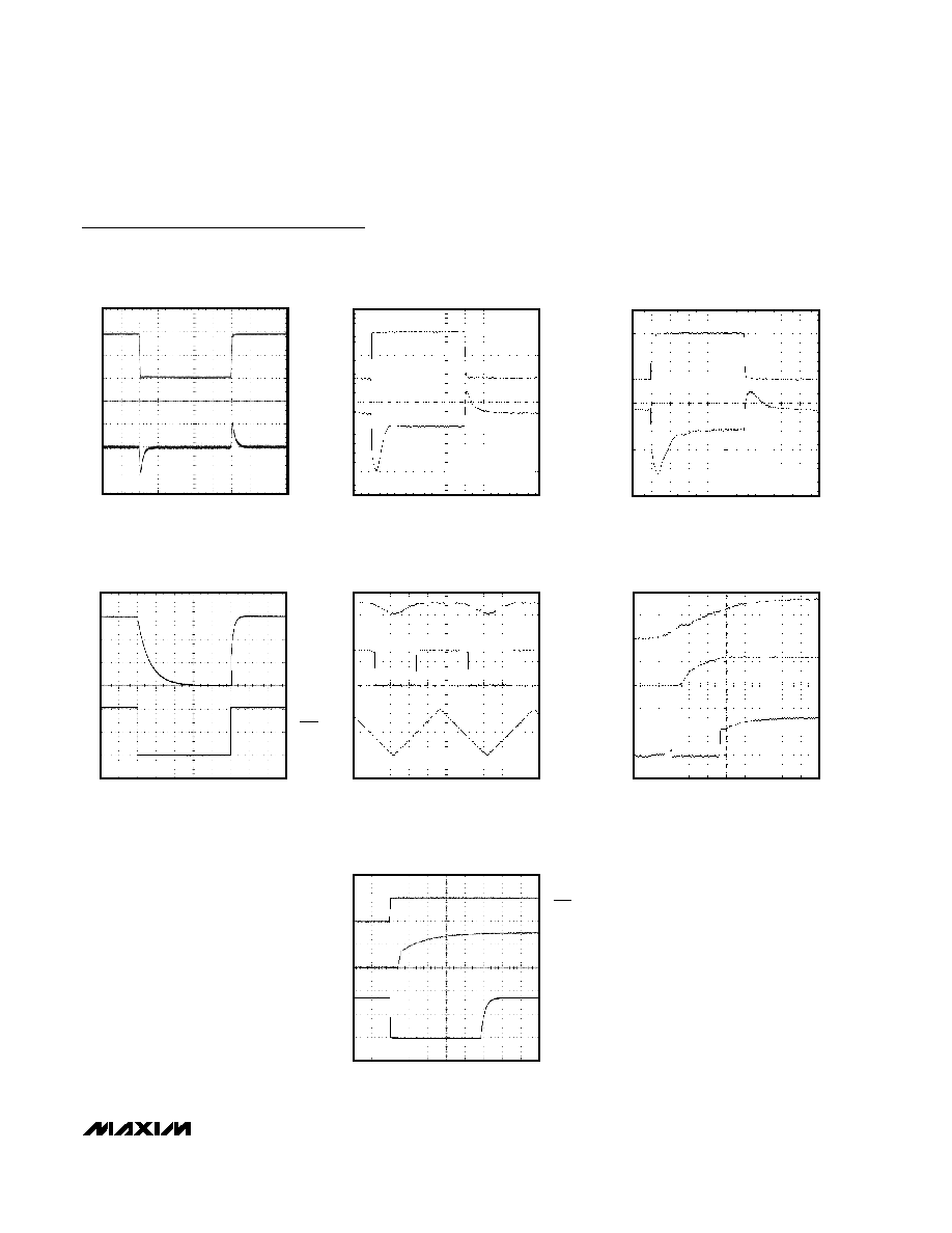
LINE-TRANSIENT RESPONSE
5V
4V
3.00V
2.98V
3.02V
V
IN
V
OUT
MAX8885toc13
R
OUT
= 60
5
µs/div
LOAD-TRANSIENT RESPONSE
3.05V
3.0V
0
50mA
V
OUT
25mV/div
I
LOAD
25mA/div
MAX8885toc14
V
IN
= V
OUT
+
0.5V
C
IN
= 1
µF
100
µs/div
SHUTDOWN DELAY
3V
0
0
2V
V
OUT
1V/div
MAX8885toc16
V
SHDN
1V/div
R
LOAD
= 60
200
µs/div
POK OUTPUT
0
0
2V
3V
4V
V
POK
2V/div
V
OUT
2V/div
MAX8885toc17
V
IN
1V/div
10ms/div
POK STARTUP RESPONSE
5V
2.5V
0
2.5V
0
0
2.5V
5V
V
POK
2.5V/div
V
OUT
2.5V/div
MAX8885toc18
V
IN
2.5V/div
Typical Operating Characteristics (continued)
(MAX8885EUK30, V
IN
= +3.6V, C
IN
= 1µF, C
OUT
= 4.7µF, SHDN = I
N
, T
A
= +25∞C, unless otherwise noted.)
10
µs/div
POK AND SHUTDOWN RESPONSE
2V
0
2V
0
0
2V
4V
V
POK
V
OUT
MAX8885toc19
V
SHDN
R
LOAD
= 60
5
µs/div
LOAD-TRANSIENT RESPONSE
NEAR DROPOUT
3.05V
3.0V
0
50mA
MAX8885toc15
V
IN
= V
OUT
+
0.1V
C
IN
= 1
µF
I
LOAD
25mA/div
V
OUT
25mV/div
MAX8885