 | –≠–ª–µ–∫—Ç—Ä–æ–Ω–Ω—ã–π –∫–æ–º–ø–æ–Ω–µ–Ω—Ç: MAX9021 | –°–∫–∞—á–∞—Ç—å:  PDF PDF  ZIP ZIP |
General Description
The MAX9021/MAX9022/MAX9024 single/dual/quad
comparators are optimized for low-power consumption
while still providing a fast output response. They are
designed for single-supply applications from 2.5V to
5.5V, but can also operate from dual supplies. These
comparators have a 3µs propagation delay and con-
sume 2.8µA of supply current per comparator over the
-40∞C to +125∞C operating temperature range. The
combination of low-power, single-supply operation
down to 2.5V, and ultra-small footprint makes these
devices ideal for portable applications.
The MAX9021/MAX9022/MAX9024 have 4mV of built-in
hysteresis to provide noise immunity and prevent oscil-
lations even with a slow-moving input signal. The input
common-mode range extends from the negative supply
to within 1.1V of the positive supply. The design of the
comparator-output stage substantially reduces switch-
ing current during output transitions, eliminating power-
supply glitches.
The MAX9021 single comparator is available in tiny 5-
pin SC70 and SOT23 packages. The MAX9022 dual
comparator is available in 8-pin SOT23, µMAX, and SO
packages, and the MAX9024 quad comparator is avail-
able in 14-pin TSSOP and SO packages.
Applications
Features
o Low-Cost Solution Available in Space-Saving
SC70 Packages (Half the Size of SOT23)
o Low 2.8µA Supply Current
o 3µs Propagation Delay
o Internal 4mV Comparator Hysteresis
o Comparator Output Swings Rail-to-Rail
Æ
o 2.5 to 5.5V Single-Supply Voltage Range
o No Phase Reversal for Overdriven Inputs
o Space-Saving Packages
5-Pin SC70 (MAX9021)
8-Pin SOT23 (MAX9022)
8-Pin µMAX (MAX9022)
14-Pin TSSOP (MAX9024)
MAX9021/MAX9022/MAX9024
Micropower, Ultra-Small, Single/Dual/Quad,
Single-Supply Comparators
________________________________________________________________ Maxim Integrated Products
1
TOP VIEW
V
SS
OUT
IN-
1
5
V
DD
IN+
MAX9021
SC70/SOT23
2
3
4
INB-
INB+
V
SS
1
2
8
7
V
DD
OUTB
INA-
INA+
OUTA
S0T23/
µMAX/SO
3
4
6
5
MAX9022
14
13
12
11
10
9
8
1
2
3
4
5
6
7
OUTD
IND-
IND+
V
SS
V
DD
INA+
INA-
OUTA
MAX9024
INC+
INC-
OUTC
OUTB
INB-
INB+
TSSOP/SO
Pin Configurations
19-1842; Rev 1; 7/01
Ordering Information
Battery-Powered
Portable Systems
Mobile Communications
Sensor-Signal Detection
Photodiode Preamps
Digital Line Receivers
Keyless Entry Systems
Threshold Detectors/
Discriminators
Typical Application Circuit appears at end of data sheet.
PART
TEMP RANGE
PIN-PACKAGE
MAX9021AXK-T
-40
∞C to +125∞C
5 SC70-5
MAX9021AUK-T
-40
∞C to +125∞C
5 SOT23-5
MAX9022AKA-T
-40
∞C to +125∞C
8 SOT23-8
MAX9022AUA
-40
∞C to +125∞C
8 µMAX
MAX9022ASA
-40
∞C to +125∞C
8 SO
MAX9024AUD
-40
∞C to +125∞C
14 TSSOP
MAX9024ASD
-40
∞C to +125∞C
14 SO
Rail-to-Rail is a registered trademark of Nippon Motorola, Ltd.
For pricing, delivery, and ordering information, please contact Maxim/Dallas Direct! at
1-888-629-4642, or visit Maxim's website at www.maxim-ic.com.
MAX9021/MAX9022/MAX9024
Micropower, Ultra-Small, Single/Dual/Quad,
Single-Supply Comparators
2
_______________________________________________________________________________________
ABSOLUTE MAXIMUM RATINGS
Stresses beyond those listed under "Absolute Maximum Ratings" may cause permanent damage to the device. These are stress ratings only, and functional
operation of the device at these or any other conditions beyond those indicated in the operational sections of the specifications is not implied. Exposure to
absolute maximum rating conditions for extended periods may affect device reliability.
Supply Voltage (V
DD
to V
SS
) ....................................-0.3V to +6V
Voltage Inputs (IN+, IN- to V
SS
). ................-0.3V to (V
DD
+ 0.3V)
Differential Input Voltage (IN+ to IN-)....................................6.6V
Output Short-Circuit Duration ..................2s to Either V
DD
or V
SS
Current into Any Pin ............................................................20mA
Continuous Power Dissipation (T
A
= +70∞C)
5-Pin SC70 (derate 3.1mW/∞C above +70∞C) ...............247mW
5-Pin SOT23 (derate 7.1mW/∞C above +70∞C).............571mW
8-Pin SOT23 (derate 9.1mW/∞C above +70∞C).............727mW
8-Pin µMAX (derate 4.5mW/∞C above +70∞C) ..............362mW
8-Pin SO (derate 5.88mW/∞C above +70∞C).................471mW
14-Pin TSSOP (derate 9.1mW/∞C above +70∞C) ..........727mW
14-Pin SO (derate 8.3mW/∞C above +70.......................667mW
Operating Temperature Range
Automotive Application...................................-40∞C to +125∞C
Junction Temperature ......................................................+150∞C
Storage Temperature Range .............................-65∞C to +150∞C
Lead Temperature (soldering, 10s) .................................+300∞C
PARAMETER
SYMBOL
CONDITIONS
MIN
TYP
MAX
UNITS
Operating Voltage Range
V
DD
Guaranteed by PSRR test
2.5
5.5
V
S up p l y C ur r ent P er C om p ar ator I
DD
2.8
5
µA
Input Offset Voltage
V
OS
(Note 2)
±1
±8
mV
Input Offset Voltage
Temperature Coefficient
TCV
OS
±1
µV/
∞C
Hysteresis
(Note 3)
4
mV
Input Bias Current
I
BIAS
3
80
nA
Input Offset Current
I
OS
±2
±60
nA
Common-Mode Voltage Range
V
CM
Guaranteed by CMRR test
V
SS
V
DD
- 1.1
V
C om m on- M od e Rej ecti on Rati o
CMRR
V
S S
V
C M
( V
D D
- 1.1V ) , V
D D
= 5.5V
70
100
d B
Power-Supply Rejection Ratio
PSRR
V
DD
= 2.5V to 5.5V
60
80
dB
I
SOURCE
= 10µA
2
V
OH
= V
DD
- V
OUT,
(V
IN+
- V
IN-
)
20mV
I
SOURCE
= 4mA
160
400
I
SINK
= 10µA
2
Output-Voltage Swing
V
OL
, V
OH
V
OL
= V
OUT
- V
SS,
(V
IN-
- V
IN+
)
20mV
I
SINK
= 4mA
180
400
mV
Output Short-Circuit Current
I
SC
50
m A
V
OD
= 10mV
8
Propagation Delay
t
pd+
, t
pd
-
R
L
= 10k
,
C
L
= 15pF (Note 4)
V
OD
= 100mV
3
µs
Rise and Fall Time
t
R
, t
F
R
L
= 10k
, C
L
= 15pF (Note 5)
20
ns
Power-On Time
R
L
= 10k
, C
L
= 15pF
150
ns
Maximum Capacitive Load
C
L
No sustained oscillations
150
pF
Note 1: All devices are production tested at 25∞C. All temperature limits are guaranteed by design.
Note 2: Comparator Input Offset is defined as the center of the hysteresis zone.
Note 3: Hysteresis is defined as the difference of the trip points required to change comparator output states.
Note 4: V
OD
is the overdrive voltage beyond the offset and hysteresis-determined trip points.
Note 5: Rise and fall times are measured between 10% and 90% at OUT.
ELECTRICAL CHARACTERISTICS
(V
DD
= 5V, V
SS
= 0, V
CM
= 0, T
A
= -40∞C to +125∞C, unless otherwise noted. Typical values are at T
A
= +25∞C.) (Note 1)
MAX9021/MAX9022/MAX9024
Micropower, Ultra-Small, Single/Dual/Quad,
Single-Supply Comparators
_______________________________________________________________________________________
3
Typical Operating Characteristics
(V
DD
= 5V, V
SS
= 0, V
CM
= 0, R
L
= 10k
, C
L
= 15pF, V
OD
= 100mV, T
A
= +25∞C, unless otherwise noted.)
3.0
2.9
2.8
2.7
2.6
2
4
3
5
6
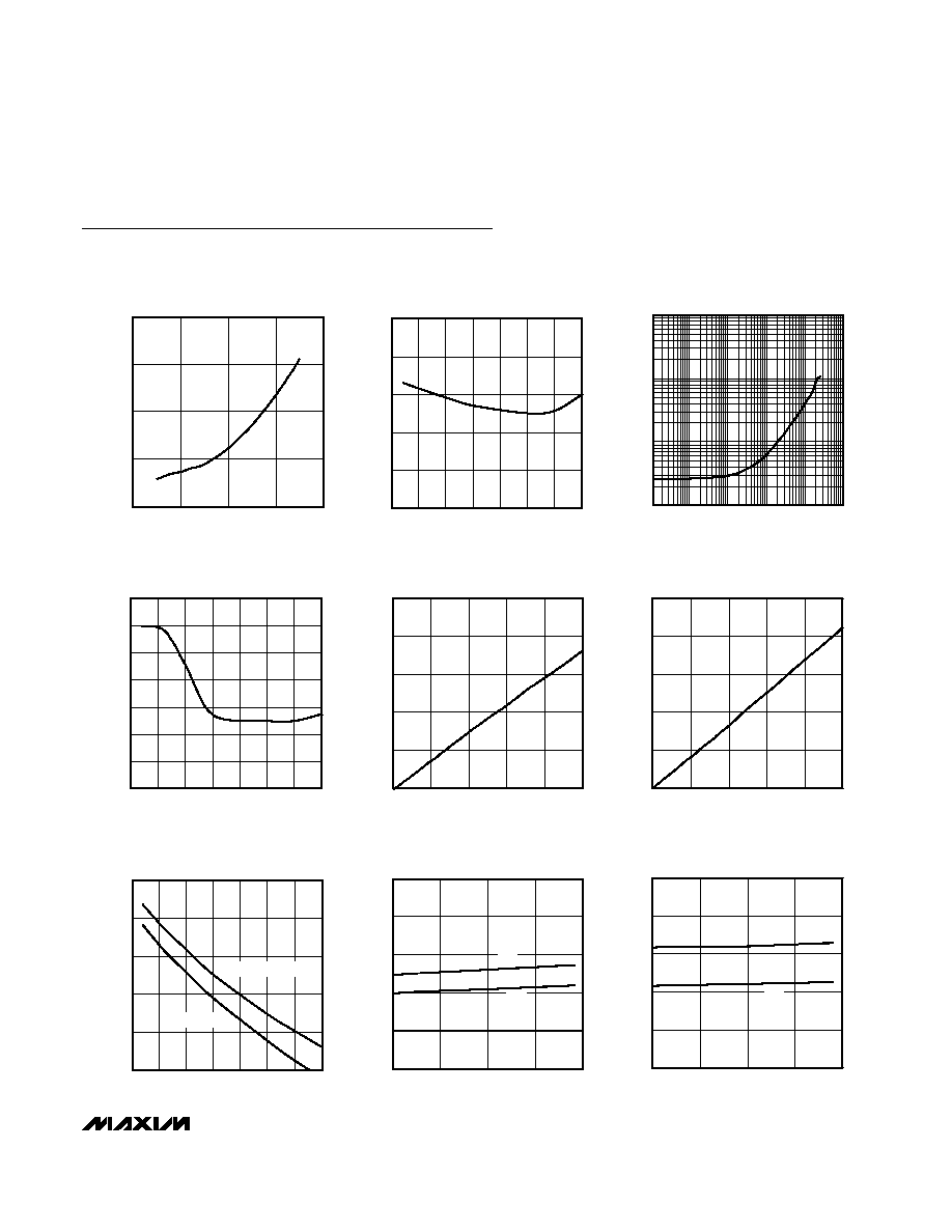
SUPPLY CURRENT
vs. SUPPLY VOLTAGE
MAX9021/2/4 toc01
SUPPLY VOLTAGE (V)
SUPPLY CURRENT (
µ
A)
2.5
2.6
2.8
2.7
2.9
3.0
-50
0
-25
25
50
75
100
125
SUPPLY CURRENT vs. TEMPERATURE
MAX9021/2/4 toc02
TEMPERATURE (
∞C)
SUPPLY CURRENT (
µ
A)
1000
1
0.01
1
1000
SUPPLY CURRENT
vs. OUTPUT TRANSITION FREQUENCY
10
100
MAX9021/2/4 toc03
OUTPUT TRANSITION FREQUENCY (kHz)
SUPPLY CURRENT (
µ
A)
0.1
10
100
0
0.4
0.2
0.8
0.6
1.2
1.0
1.4
-50
0
25
-25
50
75
100
125
INPUT OFFSET VOLTAGE
vs. TEMPERATURE
MAX9021/2/4 toc04
TEMPERATURE (
∞C)
INPUT OFFSET VOLTAGE (mV)
0
100
200
300
400
500
0
4
2
6
8
10
OUTPUT HIGH VOLTAGE
vs. SOURCE CURRENT
MAX9021/2/4 toc05
SOURCE CURRENT (mA)
(V
DD
- V
OUT
) (mV)
0
100
200
300
400
500
0
4
2
6
8
10
OUTPUT LOW VOLTAGE
vs. SINK CURRENT
MAX9021/2/4 toc06
SINK CURRENT (mA)
OUTPUT LOW VOLTAGE (mV)
40
45
55
50
60
65
-50
0
-25
25
50
75
100
125
OUTPUT SHORT-CIRCUIT CURRENT
vs. TEMPERATURE
MAX9021/2/4 toc07
TEMPERATURE (
∞C)
OUTPUT SHORT-CIRCUIT CURRENT (mA)
SOURCE CURRENT
SINK CURRENT
0
1
2
3
4
5
0
PROPAGATION DELAY vs. CAPACITIVE LOAD
(V
DD
= 2.7V)
MAX9021/2/4 toc08
CAPACITIVE LOAD (pF)
PROPAGATION DELAY (
µ
s)
t
PD
-
t
PD
+
500
1000
1500
2000
0
1
2
3
4
5
PROPAGATION DELAY vs. CAPACITIVE LOAD
(V
DD
= 5V)
MAX9021/2/4 toc09
CAPACITIVE LOAD (pF)
PROPAGATION DELAY (
µ
s)
t
PD
-
0
500
1000
1500
2000
t
PD
+
MAX9021/MAX9022/MAX9024
Micropower, Ultra-Small, Single/Dual/Quad,
Single-Supply Comparators
4
_______________________________________________________________________________________
Typical Operating Characteristics (continued)
(V
DD
= 5V, V
SS
= 0, V
CM
= 0, R
L
= 10k
, C
L
= 15pF, V
OD
= 100mV, T
A
= +25∞C, unless otherwise noted.)
0
1
3
2
4
5
-50
0
-25
25
50
75
100
125
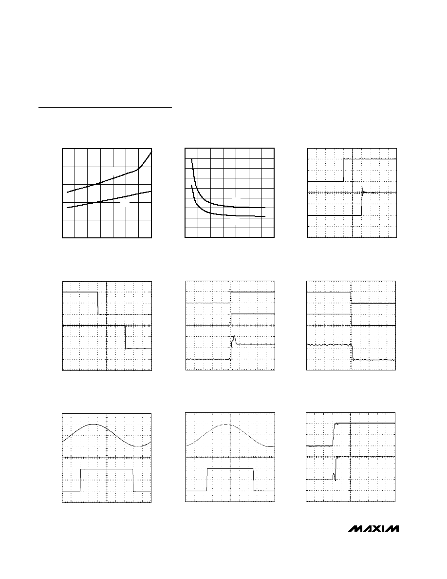
PROPAGATION DELAY
vs. TEMPERATURE
MAX9021/2/4 toc10
TEMPERATURE (
∞C)
PROPAGATION DELAY (
µ
s)
t
PD
-
t
PD
+
0
2
1
5
4
3
8
7
6
9
0
40
60
20
80
100
120
140
PROPAGATION DELAY
vs. INPUT OVERDRIVE VOLTAGE
MAX9021/2/4 toc11
INPUT OVERDRIVE VOLTAGE (mV)
PROPAGATION DELAY (
µ
s)
t
PD
+
t
PD
-
PROPAGATION DELAY (t
PD+
)
MAX9021/2/4 toc12
1
µs/div
IN+
100mV/div
V
OUT
2.5V/div
PROPAGATION DELAY (t
PD-
)
MAX9021/2/4 toc13
1
µs/div
IN+
100mV/div
V
OUT
2.5V/div
OUTPUT SWITCHING CURRENT, RISING
MAX9021/2/4 toc14
20
µs/div
IN+ - IN -
200mV/div
V
OUT
5V/div
SWITCHING
CURRENT
400
µA/div
OUTPUT SWITCHING CURRENT, FALLING
MAX9021/2/4 toc15
20
µs/div
IN+ - IN-
200mV/div
V
OUT
5V/div
SWITCHING
CURRENT
400
µA/div
10kHz RESPONSE
(V
OD
= 10mV)
MAX9021/2/4 toc16
10
µs/div
IN+ - IN -
10mV/div
OUT
2.5V/div
10kHz RESPONSE
(V
OD
= 100mV)
MAX9021/2/4 toc17
10
µs/div
IN+ - IN-
100mV/div
OUT
2.5V/div
POWER-UP TIME
MAX9021/2/4 toc18
2
µs/div
V
DD
2.5V/div
V
OUT
2.5V/div
MAX9021/MAX9022/MAX9024
Micropower, Ultra-Small, Single/Dual/Quad,
Single-Supply Comparators
_______________________________________________________________________________________
5
Detailed Description
The MAX9021/MAX9022/MAX9024 are single/dual/
quad, low-cost, low-power comparators that consume
only 2.8µA and provide a propagation delay, t
PD
, typi-
cally 3µs. They have an operating-supply voltage from
2.5V to 5.5V when operating from a single supply and
from ±1.25V to ±2.75V when operating from dual power
supplies. Their common-mode input voltage range
extends from the negative supply to within 1.1V of the
positive supply. Internal hysteresis ensures clean out-
put switching, even with slow-moving input signals.
Applications Information
Adding Hysteresis
Hysteresis extends the comparator's noise margin by
increasing the upper threshold and decreasing the
lower threshold. A voltage-divider from the compara-
tor's output sets the trip voltage. Therefore, the trip volt-
age is related to the output voltage.
These comparators have 4mV internal hysteresis.
Additional hysteresis can be generated with two resis-
tors, using positive feedback (Figure 1). Use the follow-
ing procedure to calculate resistor values:
1) Find the trip points of the comparator using these for-
mulas:
V
TH
= V
REF
+ ((V
DD
- V
REF
)R2) / (R1 + R2)
V
TL
= V
REF
(1 - (R2 / (R1 + R2))
where V
TH
is the threshold voltage at which the com-
parator switches its output from high to low as V
IN
rises above the trip point. V
TL
is the threshold volt-
age at which the comparator switches its output from
low to high as V
IN
drops below the trip point.
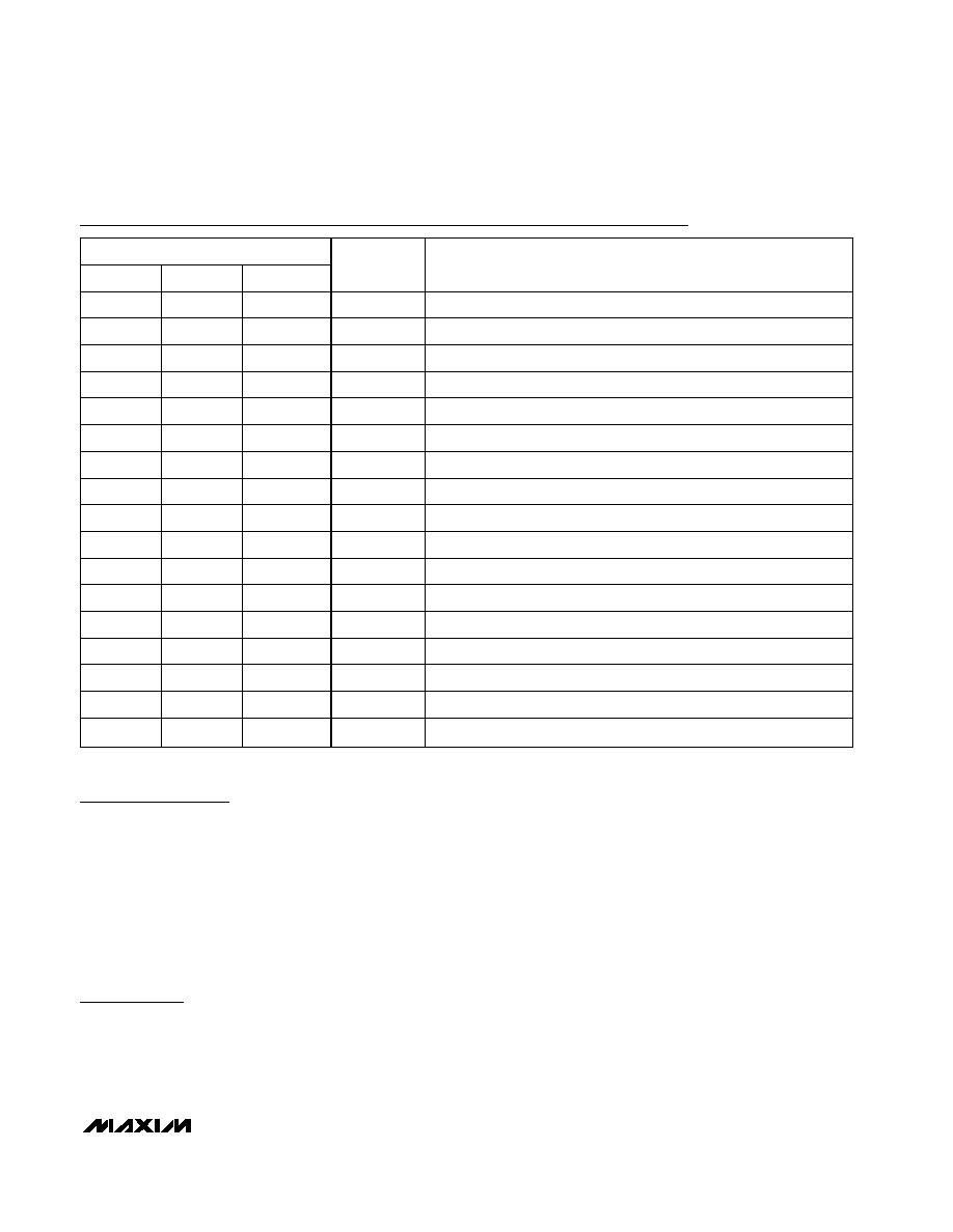
Pin Description
PIN
M A X9 0 2 1
M A X9 0 2 2
M A X9 0 2 4
NAME
FUNCTION
1
--
--
IN+
Comparator Noninverting Input
2
4
11
V
SS
Negative Supply Voltage
3
--
--
IN-
Comparator Inverting Input
4
--
--
OUT
Comparator Output
5
8
4
V
DD
Positive Supply Voltage. Bypass with a 0.1µF capacitor to GND.
--
1
1
OUTA
Comparator A Output
--
2
2
INA-
Comparator A Inverting Input
--
3
3
INA+
Comparator A Noninverting Input
--
5
5
INB+
Comparator B Noninverting Input
--
6
6
INB-
Comparator B Inverting Input
--
7
7
OUTB
Comparator B Output
--
--
8
OUTC
Comparator C Output
--
--
9
INC-
Comparator C Inverting Input
--
--
10
INC+
Comparator C Noninverting Input
--
--
12
IND+
Comparator D Noninverting Input
--
--
13
IND-
Comparator D Inverting Input
--
--
14
OUTD
Comparator D Output