 | ÐлекÑÑоннÑй компоненÑ: MAX9032 | СкаÑаÑÑ:  PDF PDF  ZIP ZIP |
Äîêóìåíòàöèÿ è îïèñàíèÿ www.docs.chipfind.ru
General Description
The MAX9030/MAX9031/MAX9032/MAX9034 single/
dual/quad comparators are optimized for single-supply
applications from +2.5V to +5.5V but can also be oper-
ated from dual supplies. These comparators have a
188ns propagation delay and consume 35µA of supply
current per comparator over the -40°C to +125°C oper-
ating temperature range. The combination of low-
power, single-supply operation down to +2.5V, and
ultra-small footprint makes these devices ideal for
portable applications.
The MAX9030 is a low-cost single comparator with
shutdown. The MAX9031, MAX9032, and MAX9034 are
low-cost single, dual, and quad comparators without
shutdown, respectively. The comparators' 4mV of built-
in hysteresis provides noise immunity and prevents
oscillations even with a slow-moving input signal. The
input common-mode range extends from the negative
supply to within 1.1V of the positive supply. The design
of the comparator output stage substantially reduces
switching current during output transitions, virtually
eliminating power-supply glitches.
The MAX9030 single comparator with shutdown is avail-
able in the space-saving 6-pin SC70 and SOT23 pack-
ages. The MAX9031 single comparator is available in tiny
5-pin SC70 and SOT23 packages. The MAX9032 dual
comparator is available in 8-pin SOT23 and µMAX pack-
ages, and the MAX9034 quad comparator is available in
a 14-pin TSSOP package.
________________________Applications
Features
o Low-Cost Solution Available in Space-Saving
SC70 Packages (MAX9030/MAX9031)
o +2.5 to +5.5V Single-Supply Voltage Range
o Comparator Output Swings Rail-to-Rail
®
o Internal 4mV Comparator Hysteresis
o 188ns Propagation Delay
o Low 35µA Supply Current
o No Phase Reversal for Overdriven Inputs
o Space-Saving Packages
5-Pin SC70 (MAX9031)
6-Pin SC70 (MAX9030)
8-Pin SOT23 (MAX9032)
14-Pin TSSOP (MAX9034)
MAX9030/MAX9031/MAX9032/MAX9034
Low-Cost, Ultra-Small, Single/Dual/Quad
Single-Supply Comparators
________________________________________________________________ Maxim Integrated Products
1
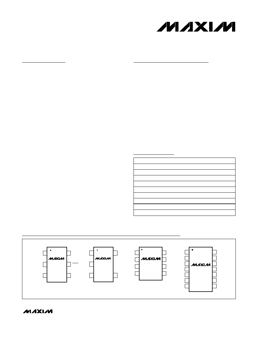
TOP VIEW
V
SS
OUT
IN-
1
5
V
DD
IN+
MAX9031
SC70-5/SOT23-5
2
3
4
INB-
INB+
V
SS
1
2
8
7
V
DD
OUTB
INA-
INA+
OUTA
SOT23-8/
µMAX-8/
SO-8
3
4
6
5
MAX9032
14
13
12
11
10
9
8
1
2
3
4
5
6
7
OUTD
IND-
IND+
V
SS
V
DD
INA+
INA-
OUTA
MAX9034
INC+
INC-
OUTC
OUTB
INB-
INB+
TSSOP-14/SO-14
V
SS
OUT
IN-
1
6
V
DD
5
IN+
MAX9030
SC70-6/SOT23-6
2
3
4
SHDN
Pin Configurations
19-1767; Rev 0; 10/00
Ordering Information
*Future productcontact factory for availability.
Battery-Powered
Portable Systems
Mobile Communications
Sensor Signal Detection
Photodiode Preamps
Digital Line Receivers
Keyless Entry Systems
Threshold Detectors/
Discriminators
Typical Application Circuit appears at end of data sheet.
PART
TEMP. RANGE
PIN-PACKAGE
M A X9 0 3 0 AX T- T
-40
°C to +125°C
6 SC70
MAX9030AUT- T -40
°C to +125°C
6 SOT23
MAX9031AXK- T -40
°C to +125°C
5 SC70
MAX9031AUK- T -40
°C to +125°C
5 SOT23
M A X 9 0 3 2 A KA - T -40
°C to +125°C
8 SOT23
MAX9032AUA*
-40
°C to +125°C
8 µMAX
MAX9032ASA
-40
°C to +125°C
8 SO
M A X9 0 3 4 AUD
-40
°C to +125°C
14 TSSOP
MAX9034AS D
-40
°C to +125°C
14 SO
Rail-to-Rail is a registered trademark of Nippon Motorola, Ltd.
For price, delivery, and to place orders, please contact Maxim Distribution at 1-888-629-4642,
or visit Maxim's website at www.maxim-ic.com.
MAX9030/MAX9031/MAX9032/MAX9034
Low-Cost, Ultra-Small, Single/Dual/Quad
Single-Supply Comparators
2
_______________________________________________________________________________________
ABSOLUTE MAXIMUM RATINGS
ELECTRICAL CHARACTERISTICS
(V
DD
= +5V, V
SS
= 0, V
CM
= 0, V
SHDN
= +5V (Note 1), T
A
= -40°C to +125°C, unless otherwise noted. Typical values are at
T
A
= +25°C.) (Note 2)
Stresses beyond those listed under "Absolute Maximum Ratings" may cause permanent damage to the device. These are stress ratings only, and functional
operation of the device at these or any other conditions beyond those indicated in the operational sections of the specifications is not implied. Exposure to
absolute maximum rating conditions for extended periods may affect device reliability.
Supply Voltage (V
DD
to V
SS
) ....................................-0.3V to +6V
Voltage Inputs (IN+, IN- to V
SS
). ................-0.3V to (V
DD
+ 0.3V)
Differential Input Voltage (IN+ to IN-) .................................+6.6V
Output Short-Circuit
Duration ...............................................2s to Either V
DD
or V
SS
Current into Any Pin ............................................................20mA
Continuous Power Dissipation (T
A
= +70°C) ...............................
5-Pin SC70 (derate 3.1mW/°C above +70°C) ...............247mW
5-Pin SOT23 (derate 7.1mW/°C above +70°C).............571mW
6-Pin SC70 (derate 3.1mW/°C above +70°C) ...............245mW
6-Pin SOT23 (derate 8.7mW/°C above +70°C).............696mW
8-Pin SOT23 (derate 9.1mW/°C above +70°C).............727mW
8-Pin µMAX (derate 4.5mW/°C above +70°C) ..............362mW
8-Pin SO (derate 5.88mW/°C above +70°C).................471mW
14-Pin TSSOP (derate 9.1mW/°C above +70°C) ..........727mW
14-Pin SO (derate 8.33mW/°C above +70°C)...............667mW
Operating Temperature Range
Automotive Application...................................-40°C to +125°C
Junction Temperature ......................................................+150°C
Storage Temperature Range .............................-65°C to +150°C
Lead Temperature (soldering, 10s) ................................ +300°C
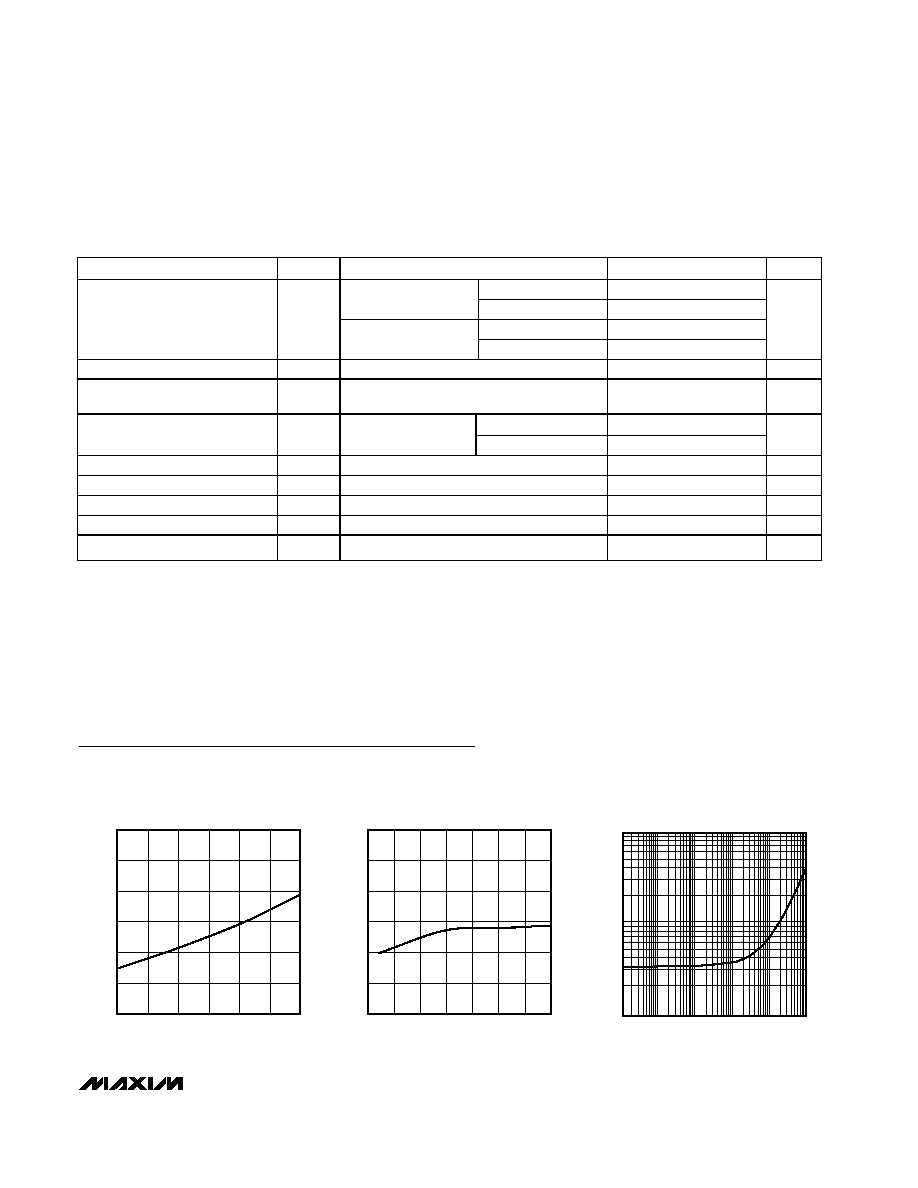
PARAMETER
SYMBOL
CONDITIONS
MIN
TYP
MAX
UNITS
Operating Voltage Range
V
DD
Guaranteed by PSRR test
2.5
5.5
V
S upp l y C ur rent p er C om par ator I
DD
35
55
µA
Supply Current in Shutdown
V
S HDN
= 0 (Note 1)
0.05
1
µA
Shutdown Input Bias Current
V
S HDN
= 0 to V
DD
(Note 1)
0.1
2.5
µA
Shutdown Logic High
(Note 1)
0.7
× V
D D
V
Shutdown Logic Low
(Note 1)
0.3
× V
D D
V
Input Offset Voltage
V
OS
(Note 3)
±1
±5
mV
Input Offset Voltage
Temperature Coefficient
TCV
OS
±1
µV/
°C
Hysteresis
(Note 4)
4
mV
Input Bias Current
I
BIAS
8
80
nA
Input Offset Current
I
OS
±2
±60
nA
Common-Mode Voltage Range
V
CM
Guaranteed by CMRR test
V
SS
V
DD
- 1.1
V
C om m on- M od e Rej ecti on Rati o
CMRR
V
S S
V
C M
( V
D D
- 1.1V ) , V
D D
= + 5.5V 72
100
d
B
Power-Supply Rejection Ratio
PSRR
V
DD
= +2.5V to +5.5V
72
100
dB
MAX9030/MAX9031/MAX9032/MAX9034
Low-Cost, Ultra-Small, Single/Dual/Quad
Single-Supply Comparators
_______________________________________________________________________________________
3
ELECTRICAL CHARACTERISTICS (continued)
(V
DD
= +5V, V
SS
= 0, V
CM
= 0, V
SHDN
= +5V (Note 1), T
A
= -40°C to +125°C, unless otherwise noted. Typical values are at
T
A
= +25°C.) (Note 2)
PARAMETER
SYMBOL
CONDITIONS
MIN
TYP
MAX
UNITS
I
SOURCE
= 10µA
2
V
OH
= V
DD
- V
OUT
,
(V
IN+
- V
IN-
)
20mV
I
SOURCE
= 4mA
165
400
I
SINK
= 10µA
2
Output Voltage-Swing
V
OL
, V
OH
V
OL
= V
OUT
- V
SS
,
(V
IN-
- V
IN+
)
20mV
I
SINK
= 4mA
165
400
mV
Output Short-Circuit Current
I
SC
45
m A
Shutdown Mode Output
Leakage
V
SHDN
(0.3 × V
DD
), V
OUT
= 0 to V
DD
(Note 1)
±0.01
±3.5
µA
V
OD
= 10mV
228
Propagation Delay
t
P D +
, t
P D -
R
L
= 10k
,
C
L
= 15pF (Note 5)
V
OD
= 100mV
188
ns
Rise/Fall-Time
t
R
, t
F
V
DD
= +5V, R
L
= 10k
, C
L
= 15pF (Note 6)
20
ns
Shutdown Delay Time ON/OFF
(Note 1)
40
ns
Shutdown Delay Time OFF/ON
(Note 1)
400
ns
Power-On Time
R
L
= 10k
, C
L
= 15pF
200
ns
Maximum Capacitive Load
C
L
No sustained oscillations
150
pF
Note 1: MAX9030 only.
Note 2: All devices are production tested at +25°C. All temperature limits are guaranteed by design.
Note 3: Comparator Input Offset is defined as the center of the hysteresis zone.
Note 4: Hysteresis is defined as the difference of the trip points required to change comparator output states.
Note 5: V
OD
is the overdrive that is beyond the offset and hysteresis-determined trip points.
Note 6: Rise and fall times are measured between 10% and 90% at OUT.
Typical Operating Characteristics
(V
DD
= +5V, V
SS
= 0, V
CM
= 0, R
L
= 10k
, C
L
= 15pF, VOD= 100mV, T
A
= +25°C, unless otherwise noted.)
28
32
30
36
34
38
40
2.5
3.5
4.0
3.0
4.5
5.0
5.5
SUPPLY CURRENT
vs. SUPPLY VOLTAGE
MAX9030/1/2/4 toc01
SUPPLY VOLTAGE (V)
SUPPLY CURRENT (
µ
A)
32
34
33
36
35
37
38
-50
25
50
-25
0
75
100
125
SUPPLY CURRENT
vs. TEMPERATURE
MAX9030/1/2/4 toc02
TEMPERATURE (
°C)
SUPPLY CURRENT (
µ
A)
1000
10
10
100
OUTPUT TRANSITION FREQUENCY (Hz)
SUPPLY CURRENT (
µ
A)
SUPPLY CURRENT
vs. OUTPUT TRANSITION FREQUENCY
100
1k
10k
100k
1M
MAX9030/1/2/4 toc03
MAX9030/MAX9031/MAX9032/MAX9034
Low-Cost, Ultra-Small, Single/Dual/Quad
Single-Supply Comparators
4
_______________________________________________________________________________________
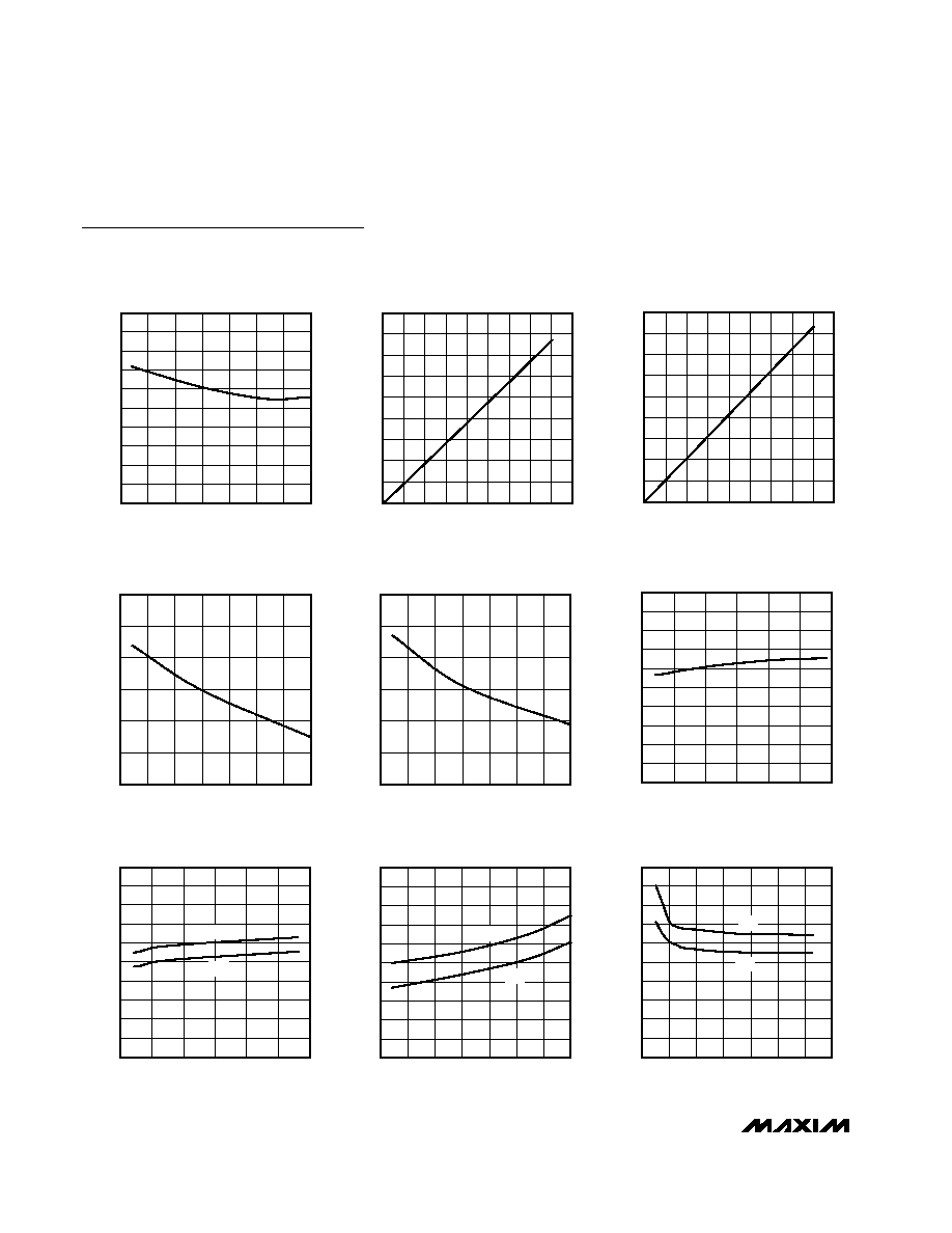
Typical Operating Characteristics (continued)
(V
DD
= +5V, V
SS
= 0, V
CM
= 0, R
L
= 10k
, C
L
= 15pF, VOD = 100mV, T
A
= +25°C, unless otherwise noted.)
-0.5
-0.2
-0.3
-0.4
0
-0.1
0.4
0.3
0.2
0.1
0.5
-50
-25
0
25
50
75
100
125
INPUT OFFSET VOLTAGE
vs. TEMPERATURE
MAX9030/1/2/4 toc04
TEMPERATURE (
°C)
INPUT OFFSET VOLTAGE (mV)
0
40
20
100
80
60
140
160
120
180
0
1.5 2.0
0.5 1.0
2.5 3.0 3.5 4.0 4.5
OUTPUT HIGH VOLTAGE
vs. SOURCE CURRENT
MAX9030/1/2/4 toc05
SOURCE CURRENT (mA)
V
DD
- V
OUT
OUTPUT HIGH VOLTAGE (mV)
0
40
20
100
80
60
140
160
120
180
0
1.5 2.0
0.5 1.0
2.5 3.0 3.5 4.0 4.5
OUTPUT LOW VOLTAGE
vs. SINK CURRENT
MAX9030/1/2/4 toc06
SINK CURRENT (mA)
OUTPUT LOW VOLTAGE (mV)
30
40
35
50
45
55
60
-50
25
50
-25
0
75
100
125
OUTPUT SHORT-CIRCUIT (SINK) CURRENT
vs. TEMPERATURE
MAX9030/1/2/4 toc07
TEMPERATURE (
°C)
SHORT-CIRCUIT SINK CURRENT (mA)
30
40
35
50
45
55
60
-50
25
50
-25
0
75
100
125
OUTPUT SHORT-CIRCUIT (SOURCE) CURRENT
vs. TEMPERATURE
MAX9030/1/2/4 toc08
TEMPERATURE (
°C)
SHORT-CIRCUIT SOURCE CURRENT (mA)
100
160
140
120
180
200
220
240
260
280
300
0
50
25
75
100
125
150
PROPAGATION DELAY vs. CAPACITIVE LOAD
(V
DD
= 2.7V)
MAX9030/1/2/4 toc09
CAPACITIVE LOAD (pF)
PROPAGATION DELAY (ns)
100
160
140
120
180
200
220
240
260
280
300
0
50
25
75
100
125
150
PROPAGATION DELAY vs. CAPACITIVE LOAD
(V
DD
= +5V)
MAX9030/1/2/4 toc10
CAPACITIVE LOAD (pF)
PROPAGATION DELAY (ns)
t
PD-
t
PD+
100
160
140
120
200
180
280
260
240
220
300
-50
-25
0
25
50
75
100
125
PROPAGATION DELAY vs. TEMPERATURE
MAX9030/1/2/4 toc11
TEMPERATURE (
°C)
PROPAGATION DELAY (ns)
t
PD-
t
PD+
50
125
100
75
175
150
275
250
225
200
300
0
20
40
60
80
100
120
140
PROPAGATION DELAY
vs. INPUT OVERDRIVE VOLTAGE
MAX9030/1/2/4 toc12
INPUT OVERDRIVE VOLTAGE (mV)
PROPAGATION DELAY (ns)
t
PD-
t
PD+
MAX9030/MAX9031/MAX9032/MAX9034
Low-Cost, Ultra-Small, Single/Dual/Quad
Single-Supply Comparators
_______________________________________________________________________________________
5
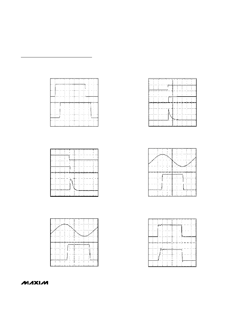
TIME (200ns/div)
PROPAGATION DELAY
MAX9030/1/2/4 toc13
OUT
2V/div
IN+ - IN-
200mV/div
TIME (2
µs/div)
OUTPUT SWITCHING CURRENT, RISING
MAX9030/1/2/4 toc14
SWITCHING
CURRENT
200
µA/div
IN+ - IN-
5V/div
OUT
5V/div
TIME (1
µs/div)
OUTPUT SWITCHING CURRENT, FALLING
MAX9030/1/2/4 toc15
SWITCHING
CURRENT
50
µA/div
IN+ - IN-
5V/div
OUT
5V/div
TIME (100ns/div)
SINUSOID 1MHz RESPONSE AT 1.25MHz
V
OD
= 100mV
MAX9030/1/2/4 toc16
IN+ - IN-
100mV/div
OUT
2V/div
TIME (100ns/div)
SINUSOID 1MHz RESPONSE AT 1.25MHz
V
OD
= 10mV
MAX9030/1/2/4 toc17
IN+ - IN-
10mV/div
OUT
2V/div
TIME (200ns/div)
POWER-UP DELAY
MAX9030/1/2/4 toc18
V
DD
OUT
2.5V/div
Typical Operating Characteristics (continued)
(V
DD
= +5V, V
SS
= 0, V
CM
= 0, R
L
= 10k
, C
L
= 15pF, VOD = 100mV, T
A
= +25°C, unless otherwise noted.)