 | –≠–ª–µ–∫—Ç—Ä–æ–Ω–Ω—ã–π –∫–æ–º–ø–æ–Ω–µ–Ω—Ç: MAX9075 | –°–∫–∞—á–∞—Ç—å:  PDF PDF  ZIP ZIP |

For free samples & the latest literature: http://www.maxim-ic.com, or phone 1-800-998-8800.
For small orders, phone 1-800-835-8769.
General Description
The MAX9075/MAX9077 single/dual comparators are
optimized for +3V and +5V single-supply applications.
These comparators have a 580ns propagation delay and
consume just 3µA per comparator. The combination of
low-power, single-supply operation down to +2.1V, and
ultra-small footprint makes these devices ideal for all
portable applications.
The MAX9075/MAX9077 have a common-mode input
voltage range of -0.2V to V
CC
- 1.2V. Unlike many com-
parators, there is no differential clamp between the
inputs, allowing the differential input voltage range to
extend Rail-to-Rail
Æ
. All inputs and outputs tolerate a
continuous short-circuit fault condition to either rail.
The design of the output stage limits supply-current
surges while switching (typical of many other compara-
tors), minimizing power consumption under dynamic
conditions. Large internal push-pull output drivers allow
rail-to-rail output swing with loads up to 2mA, making
these devices ideal for interface with TTL/CMOS logic.
The MAX9075 single comparator is available in 5-pin
SC70 and SOT23-5 packages, while the MAX9077 dual
comparator is available in 8-pin SOT23-8 and SO
packages.
Applications
Battery-Powered Systems
Threshold Detectors/Discriminators
Keyless Entry Systems
IR Receivers
Digital Line Receivers
Features
o
580ns Propagation Delay from Only 3µA
o
+2.1V to +5.5V Single-Supply Operation
o
Ground-Sensing Inputs
o
Rail-to-Rail Outputs
o
No Output Phase Inversion for Overdriven Inputs
o
No Differential Clamp Across Inputs
o
Available in Ultra-Small Packages
5-Pin SC70 (MAX9075)
8-Pin SOT23 (MAX9077)
MAX9075/MAX9077
Low-Cost, Ultra-Small, 3µA
Single-Supply Comparators
________________________________________________________________
Maxim Integrated Products
1
19-1547; Rev 0; 10/99
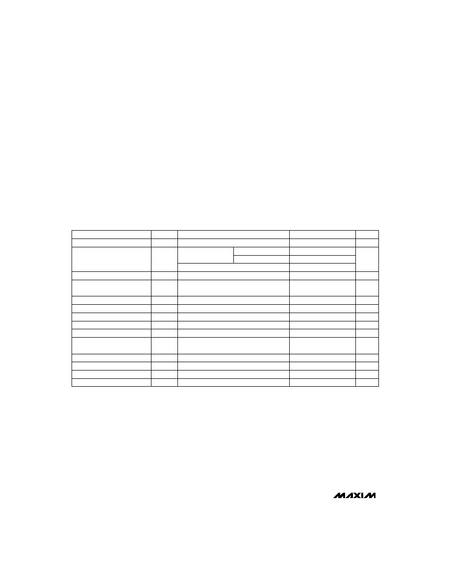
PART
MAX9075
EXK-T
MAX9075EUK-T
MAX9077
EKA-T
-40∞C to +85∞C
-40∞C to +85∞C
-40∞C to +85∞C
TEMP. RANGE
PIN-
PACKAGE
5 SC70-5
5 SOT23-5
8 SOT23-8
Ordering Information
TOP
MARK
AAC
ADLX
AAAD
MAX9077ESA
-40∞C to +85∞C
8 SO
--
Typical Operating Circuit
V
CC
V
CC
OUT
GND
V
REF
IN-
IN+
V
IN
MAX9075
MAX9077
Pin Configurations
TOP VIEW
GND
IN-
IN+
1
5
V
CC
OUT
MAX9075
SC70-5/SOT23-5
2
3
4
Pin Configurations continued at end of data sheet.
V
CC
= 5V
MAX9075/MAX9077
Low-Cost, Ultra-Small, 3µA
Single-Supply Comparators
2
_______________________________________________________________________________________
ABSOLUTE MAXIMUM RATINGS
ELECTRICAL CHARACTERISTICS
(V
CC
= +5V, V
CM
= -0.2V, T
A
= T
MIN
to T
MAX
, unless otherwise noted. Typical values are at T
A
= +25∞C.) (Note 1)
Stresses beyond those listed under "Absolute Maximum Ratings" may cause permanent damage to the device. These are stress ratings only, and functional
operation of the device at these or any other conditions beyond those indicated in the operational sections of the specifications is not implied. Exposure to
absolute maximum rating conditions for extended periods may affect device reliability.
Note 1:
All devices are 100% production tested at T
A
= +25∞C. All temperature limits are guaranteed by design.
Note 2:
Inferred from CMRR. Either input can be driven to the absolute maximum limit without output inversion, as long as the other
input is within the input voltage range.
Note 3:
Guaranteed by design.
Supply Voltage
V
CC
to GND .....................................................................+6V
All Other Pins to GND...........................-0.3V to (V
CC
+ 0.3V)
Duration of Output Short Circuit to GND or V
CC
........Continuous
Continuous Power Dissipation (T
A
= +70∞C)
5-Pin SC70 (derate 2.5mW/∞C above +70∞C) ............200mW
5-Pin SOT23 (derate 7.1mW/∞C above +70∞C)..........571mW
8-Pin SOT23 (derate 5.3mW/∞C above +70∞C)..........421mW
8-Pin SO (derate 5.88mW/∞C above +70∞C)..............471mW
Operating Temperature Range ...........................-40∞C to +85∞C
Storage Temperature Range .............................-65∞C to +150∞C
Lead Temperature (soldering, 10sec) .............................+300∞C
Inferred from PSRR
C
LOAD
= 10pF
-0.2V
V
CM
(V
CC
- 1.2V)
C
LOAD
= 10pF, overdrive = 100mV
C
LOAD
= 10pF, overdrive = 100mV
V
CM
= 0 (Note 3)
V
CC
= 3V
2.1V
V
CC
5.5V
(Note 2)
I
SINK
= 2mA
I
SOURCE
= 2mA
CONDITIONS
ns
1.6
Rise/Fall Time
ns
250
t
PD-
Propagation Delay High to Low
ns
580
t
PD+
Propagation Delay Low to High
V
0.4
V
OL
OUT_ Output Voltage Low
V
V
CC
-
0.4
V
OH
OUT_ Output Voltage High
6.6
3
5.2
I
CC
V
2.1
5.5
V
CC
Operating Supply Voltage Range
Supply Current per Comparator
dB
60
82
CMRR
Common-Mode Rejection Ratio
pF
3
C
IN
Input Capacitance
nA
-5
-20
I
B
Input Bias Current
nA
1
I
OS
Input Offset Current
2.4
dB
54
77
PSRR
Power-Supply Rejection Ratio
V
-0.2
V
CC
-
1.2
V
CMR
Common-Mode Voltage Range
mV
±1
±8
V
OS
Input Offset Voltage
UNITS
MIN
TYP
MAX
SYMBOL
PARAMETER
T
A
= +25∞C
T
A
= T
MIN
to T
MAX
V
CC
= 5V
µA

MAX9075/MAX9077
Low-Cost, Ultra-Small, 3µA
Single-Supply Comparators
_______________________________________________________________________________________
3
0
1.0
0.5
2.0
1.5
2.5
3.0
0
10
5
15
20
OUTPUT VOLTAGE LOW vs.
SINK CURRENT (V
CC
= 2.1V)
MAX9075/7 toc01
SINK CURRENT (mA)
OUTPUT VOLTAGE (V)
T
A
= +85∞C
T
A
= +25∞C
T
A
= -40∞C
0
1.0
0.5
2.0
1.5
2.5
3.5
3.0
4.0
0
10
5
15
20
25
30
35
40
OUTPUT VOLTAGE LOW vs.
SINK CURRENT (V
CC
= 3V)
MAX9075/7 toc02
SINK CURRENT (mA)
OUTPUT VOLTAGE (V)
T
A
= +85∞C
T
A
= +25∞C
T
A
= -40∞C
0
2
1
4
3
5
7
6
0
20
10
30
40
50
60
70
80
90
OUTPUT VOLTAGE LOW vs.
SINK CURRENT (V
CC
= 5V)
MAX9075/7 toc03
SINK CURRENT (mA)
OUTPUT VOLTAGE (V)
T
A
= +85∞C
T
A
= +25∞C
T
A
= -40∞C
-0.5
0.5
0
1.5
1.0
2.0
2.5
0
4
2
6
8
10
12
14
16
18
OUTPUT VOLTAGE HIGH vs.
SOURCE CURRENT (V
CC
= 2.1V)
MAX9075/7 toc04
SOURCE CURRENT (mA)
OUTPUT VOLTAGE (V)
T
A
= +85∞C
T
A
= +25∞C
T
A
= -40∞C
-0.5
0.5
0
1.5
1.0
2.0
2.5
3.0
3.5
0
10
5
15
20
25
30
35
40
45
OUTPUT VOLTAGE HIGH vs.
SOURCE CURRENT (V
CC
= 3V)
MAX9075/7 toc05
SOURCE CURRENT (mA)
OUTPUT VOLTAGE (V)
T
A
= +85∞C
T
A
= +25∞C
T
A
= -40∞C
-1
1
0
3
2
4
5
6
0
20
10
30 40
50 60 70 80 90 100
OUTPUT VOLTAGE HIGH vs.
SOURCE CURRENT (V
CC
= 5V)
MAX9075/7 toc06
SOURCE CURRENT (mA)
OUTPUT VOLTAGE (V)
T
A
= +85∞C
T
A
= +25∞C
T
A
= -40∞C
20
10
0
40
30
80
70
60
50
90
-55
-35
-15
5
25
45
65
85
SHORT-CIRCUIT SINK CURRENT
vs. TEMPERATURE
MAX9075 toc07
TEMPERATURE (∞C)
SINK CURRENT (mA)
V
CC
= 5V
V
CC
= 3V
V
CC
= 2.1V
20
10
0
40
30
80
70
60
50
90
100
-55
-35
-15
5
25
45
65
85
SHORT-CIRCUIT SOURCE CURRENT
vs. TEMPERATURE
MAX9075 toc08
TEMPERATURE (∞C)
SOURCE CURRENT (mA)
V
CC
= 5V
V
CC
= 3V
V
CC
= 2.1V
1.0
0.5
0
2.0
1.5
4.0
3.5
3.0
2.5
4.5
-55
-35
-15
5
25
45
65
85
SUPPLY CURRENT vs.
TEMPERATURE (OUT = HIGH)
MAX9075 toc09
TEMPERATURE (∞C)
SUPPLY CURRENT (
µ
A)
V
CC
= 5V
V
CC
= 3V
V
CC
= 2.1V
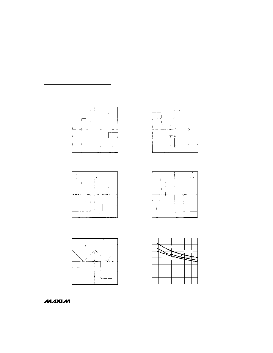
Typical Operating Characteristics
(V
CC
= +5V, V
CM
= 0, 100mV overdrive, T
A
= +25∞C, unless otherwise noted.)

MAX9075/MAX9077
Low-Cost, Ultra-Small, 3µA
Single-Supply Comparators
4
_______________________________________________________________________________________
1.0
0.5
0
2.0
1.5
4.0
3.5
3.0
2.5
-55
-35
-15
5
25
45
65
85
SUPPLY CURRENT vs.
TEMPERATURE (OUT = LOW)
MAX9075 toc10
TEMPERATURE (∞C)
SUPPLY CURRENT (
µ
A)
V
CC
= 5V
V
CC
= 3V
V
CC
= 2.1V
SUPPLY CURRENT vs.
OUTPUT TRANSITION FREQUENCY
MAX9075 toc11
TRANSITION FREQUENCY (Hz)
SUPPLY CURRENT (
µ
A)
1000
1
10
100
1
1k
10k
100k
10
100
1M
V
CC
= 2.1V
V
CC
= 5V
V
CC
= 3V
-0.6
-0.7
-0.8
-0.4
-0.5
0
-0.1
-0.2
-0.3
-55
-35
-15
5
25
45
65
85
INPUT OFFSET VOLTAGE
vs. TEMPERATURE
MAX9075 toc12
TEMPERATURE (∞C)
OFFSET VOLTAGE (mV)
V
CC
= 5V
V
CC
= 3V
V
CC
= 2.1V
0
0.2
0.1
0.4
0.3
0.6
0.5
0.7
PROPAGATION DELAY
vs. LOAD CAPACITANCE
MAX9075 toc13
LOAD CAPACITANCE (pF)
PROPAGATION DELAY (
µ
s)
0
500
1000
1500
2000
t
PD+
t
PD-
0
0.4
0.2
0.8
0.6
1.2
1.0
1.4
1.6
PROPAGATION DELAY
vs. INPUT OVERDRIVE (t
PD+
)
MAX9075 toc14
INPUT OVERDRIVE (mV)
PROPAGATION DELAY (
µ
s)
0
50
100
150
200
250
V
CC
= 5V
V
CC
= 3V
V
CC
= 2.1V
0
0.2
0.1
0.4
0.3
0.6
0.5
0.7
PROPAGATION DELAY
vs. INPUT OVERDRIVE (t
PD-
)
MAX9075 toc15
INPUT OVERDRIVE (mV)
PROPAGATION DELAY (
µ
s)
0
50
100
150
200
250
V
CC
= 5V
V
CC
= 3V
V
CC
= 2.1V
0
100
50
200
150
300
250
350
400
450
500
PROPAGATION DELAY
vs. TEMPERATURE (V
CC
= 2.1V)
MAX9075 toc16
TEMPERATURE (
∞
C)
PROPAGATION DELAY (ns)
-55
-35
-15
5
25
45
65
85
t
PD-
t
PD+
0
100
200
300
400
500
600
PROPAGATION DELAY
vs. TEMPERATURE (V
CC
= 3V)
MAX9075 toc17
TEMPERATURE (
∞
C)
PROPAGATION DELAY (ns)
-55
-35
-15
5
25
45
65
85
t
PD-
t
PD+
0
100
200
300
400
500
600
700
800
PROPAGATION DELAY
vs. TEMPERATURE (V
CC
= 5V)
MAX9075 toc18
TEMPERATURE (
∞
C)
PROPAGATION DELAY (ns)
-55
-35
-15
5
25
45
65
85
t
PD-
t
PD+
Typical Operating Characteristics (continued)
(V
CC
= +5V, V
CM
= 0, 100mV overdrive, T
A
= +25∞C, unless otherwise noted.)
MAX9075/MAX9077
Low-Cost, Ultra-Small, 3µA
Single-Supply Comparators
_______________________________________________________________________________________
5
100ns/div
PROPAGATION DELAY (t
PD+
)
MAX9075/7 toc19
50mV/div
2V/div
V
IN
V
CC
= 5V
V
OUT
100ns//div
PROPAGATION DELAY (t
PD-
)
MAX9075/7 toc20
50mV/div
2V/div
V
OUT
V
IN
V
CC
= 5V
200
µ
s/div
TRIANGLE WAVE
MAX9075/7 toc21
V
IN
V
OUT
50mV/div
1V/div
V
CC
= 3V
100ns/div
PROPAGATION DELAY (t
PD+
)
MAX9075/7 toc22
V
IN
V
OUT
50mV/div
1V/div
V
CC
= 3V
100ns/div
PROPAGATION DELAY (t
PD-
)
MAX9075/7 toc23
V
IN
V
OUT
50mV/div
1V/div
V
CC
= 3V
0
1
2
3
4
5
6
7
INPUT BIAS CURRENT
vs. TEMPERATURE
MAX9075 toc24
TEMPERATURE (
∞
C)
INPUT BIAS CURRENT (nA)
-55
-35
-15
5
25
45
65
85
V
CC
= 5V
V
CC
= 2.1V
V
CC
= 3V
Typical Operating Characteristics (continued)
(V
CC
= +5V, V
CM
= 0, 100mV overdrive, T
A
= +25∞C, unless otherwise noted.)