 | –≠–ª–µ–∫—Ç—Ä–æ–Ω–Ω—ã–π –∫–æ–º–ø–æ–Ω–µ–Ω—Ç: MAX9107 | –°–∫–∞—á–∞—Ç—å:  PDF PDF  ZIP ZIP |

MAX9107/MAX9108/MAX9109
25ns, Dual/Quad/Single, Low-Power,
TTL Comparators
________________________________________________________________ Maxim Integrated Products
1
TOP VIEW
1
2
3
4
5
6
7
8
SO
N.C.
OUT
GND
LE
V
CC
IN+
IN-
N.C.
MAX9109
1
2
3
4
5
6
7
8
SOT23/SO
V
CC
OUTB
INB-
INB+
OUTA
INA-
INA+
GND
MAX9107
14
13
12
11
10
9
8
1
2
3
4
5
6
7
OUTD
IND-
IND+
GND
V
CC
INA+
INA-
OUTA
MAX9108
INC+
INC-
OUTC
OUTB
INB-
INB+
TSSOP/SO
A
D
B
C
GND
IN-
IN+
1
6
V
CC
5
LE
OUT
MAX9109
SC70/SOT23
2
3
4
Pin Configurations
19-2045; Rev. 0; 5/01
General Description
The MAX9107/MAX9108/MAX9109 dual/quad/single,
high-speed, low-power voltage comparators are
designed for use in systems powered from a single
+5V supply. Their 25ns propagation delay (with 10mV
input overdrive) is achieved with a power consumption
of only 1.75mW per comparator. The wide input com-
mon-mode range extends from 200mV below ground
to within 1.5V of the positive supply rail.
The MAX9107/MAX9108/MAX9109 outputs are TTL-
compatible, requiring no external pullup circuitry.
These easy-to-use comparators incorporate internal
hysteresis to ensure clean output switching even when
the devices are driven by a slow-moving input signal.
The MAX9107/MAX9108/MAX9109 are higher-speed,
lower-power, lower-cost upgrades to industry-standard
comparators MAX907/MAX908/MAX909. The MAX9109
features an output latch but does not have comple-
mentary outputs.
The dual MAX9107 is available in both 8-pin SO and
SOT23 packages. The quad MAX9108 is available in
14-pin TSSOP and SO packages while the single
MAX9109 is available in an ultra-small 6-pin SC70
package, a space-saving 6-pin SOT23 package and
an 8-pin SO package.
Applications
Features
o 25ns Propagation Delay
o 350µA (1.75mW) Supply Current Per Comparator
o Single 4.5V to 5.5V Supply Operation
o Wide Input Range Includes Ground
o Low 500µV Offset Voltage
o Internal Hysteresis Provides Clean Switching
(2mV)
o TTL-Compatible Outputs
o Internal Latch (MAX9109 only)
o No Phase Reversal for Overdriven Inputs
o Space-Saving Packages:
6-Pin SC70 (MAX9109)
8-Pin SOT23 (MAX9107)
14-Pin TSSOP (MAX9108)
Ordering Information
PART
TEMP. RANGE
PIN-
PACKAGE
TOP
MARK
MAX9107EKA-T
-40∞C to +85∞C
8 SOT23-8
AAIB
MAX9107ESA
-40∞C to +85∞C
8 SO
--
MAX9108EUD
-40∞C to +85∞C
14 TSSOP
--
MAX9108ESD
-40∞C to +85∞C
14 SO
--
MAX9109EXT-T
-40∞C to +85∞C
6 SC70-6
AAU
MAX9109EUT-T
-40∞C to +85∞C
6 SOT23-6
AARU
MAX9109ESA
-40∞C to +85∞C
8 SO
--
Battery-Powered Systems
A/D Converters
Line Receivers
Threshold Detectors/
Discriminators
Sampling Circuits
Zero-Crossing Detectors
For pricing, delivery, and ordering information, please contact Maxim/Dallas Direct! at
1-888-629-4642, or visit Maxim's website at www.maxim-ic.com.

MAX9107/MAX9108/MAX9109
25ns, Dual/Quad/Single, Low-Power,
TTL Comparators
2
_______________________________________________________________________________________
Power-Supply Ranges
Supply Voltage (V
CC
to GND) ..............................................6V
Differential Input Voltage ........................-0.3V to (V
CC
+ 0.3V)
Common-Mode Input Voltage to GND ...-0.3V to (V
CC
+ 0.3V)
Latch-Enable Input Voltage
(MAX9109 only) ...................................-0.3V to (V
CC
+ 0.3V)
Output Short-Circuit Duration to V
CC
or GND ........................10s
Continuous Power Dissipation (T
A
= +70∞C)
6-Pin SC70 (derate 3.1mW/∞C above +70∞C) ..............245mW
6-Pin SOT23 (derate 8.7mW/∞C above +70∞C)............696mW
8-Pin SOT23 (derate 9.1mW/∞C above +70∞C)............727mW
8-Pin SO (derate 5.9mW/∞C above +70∞C)..................470mW
14-Pin TSSOP (derate 9.1mW/∞C above +70∞C) .........727mW
14-Pin SO (derate 8.33mW/∞C above +70∞C)..............666mW
Operating Temperature Range ...........................-40∞C to +85∞C
Storage Temperature Range .............................-65∞C to +150∞C
Lead Temperature (soldering, 10s) .................................+300∞C
ELECTRICAL CHARACTERISTICS
(V
CC
= +5V, V
CM
= 0, V
LE
= 0 (MAX9109 only), T
A
= T
MIN
to T
MAX
, unless otherwise noted. Typical values are at T
A
= +25∞C.) (Note 1)
Stresses beyond those listed under "Absolute Maximum Ratings" may cause permanent damage to the device. These are stress ratings only, and functional
operation of the device at these or any other conditions beyond those indicated in the operational sections of the specifications is not implied. Exposure to
absolute maximum rating conditions for extended periods may affect device reliability.
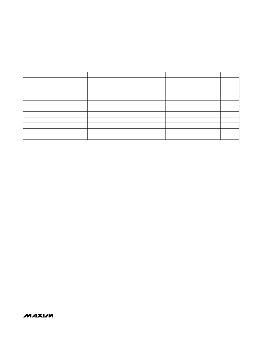
ABSOLUTE MAXIMUM RATINGS
PARAMETER
Operating Voltage Range
Input Bias Current
Input Offset Current
Common-Mode Rejection Ratio
Power-Supply Rejection Ratio
Output High Voltage
Output Low Voltage
Output Rise Time
Output Fall Time
t
f
t
r
V
OL
V
OH
PSRR
CMRR
I
OS
I
B
V
CC
SYMBOL
V
OUT
= 2.4V to 0.4V, C
L
= 10pF
V
OUT
= 0.4V to 2.4V, C
L
= 10pF
I
SINK
= 8mA
I
SINK
= 3.2mA
I
SOURCE
= 100µA
4.5V
V
CC
5.5V
V
CC
= 5.5V (Note 5)
T
A
= +25
∞C
Guaranteed by PSRR
CONDITIONS
MIN
TYP
MAX
4.5
5.5
0.5
1.6
125
350
25
80
50
1000
50
1000
3.0
3.5
0.35
0.6
0.4
12
6
ns
ns
V
V
µV/V
µV/V
nA
nA
V
UNITS
Input Hysteresis
V
HYST
(Note 3)
2
mV
Input Voltage Range
V
CMR
(Note 4)
-0.2
V
CC
- 1.5
V
mA
Supply Current Per Comparator
V
CC
= +5.5V, all outputs low
I
CC
0.35
0.7
Input Offset Voltage
V
OS
T
A
= T
MIN
to T
MAX
4.0
mV
(Note 2)
MAX9107/MAX9108/MAX9109
25ns, Dual/Quad/Single, Low-Power,
TTL Comparators
_______________________________________________________________________________________
3
ELECTRICAL CHARACTERISTICS (continued)
(V
CC
= +5V, V
CM
= 0, V
LE
= 0 (MAX9109 only), T
A
= T
MIN
to T
MAX
, unless otherwise noted. Typical values are at T
A
= +25∞C.) (Note 1)
Latch Hold Time
Latch Setup Time
Latch Input Current
Latch Input Voltage Low
Latch Input Voltage High
Propagation Delay Skew
Differential Propagation Delay
Propagation Delay
PARAMETER
SYMBOL
t
PD+,
t
PD-
t
PD
t
PD
skew
V
IH
V
IL
I
IH
, I
IL
t
s
t
h
(Note 8)
(Note 8)
(Note 8)
(Note 8)
(Note 8)
V
IN
= 100mV, V
OD
= 10mV
(Note 7)
V
IN
= 100mV, V
OD
= 10mV
(Note 6)
V
IN
= 100mV, V
OD
= 10mV
CONDITIONS
MIN
TYP
MAX
25
1
5
2.0
0.8
0.4
1
2
2
ns
ns
µA
V
V
ns
ns
ns
UNITS
Note 1:
Devices are 100% production tested at T
A
= +25∞C. All temperature limits are guaranteed by design.
Note 2:
Input Offset Voltage is defined as the center of the input-referred hysteresis zone. Specified for V
CM
= 0. See Figure 1.
Note 3:
Trip Point is defined as the input voltage required to make the comparator output change state. The difference
between upper (V
TRIP
+) and lower (V
TRIP
-) trip points is equal to the width of the input-referred hysteresis zone (V
HYST
).
Specified for an input common-mode voltage (V
CM
) of 0. See Figure 1.
Note 4:
Inferred from the CMRR test. Note that a correct logic result is obtained at the output, provided that at least one input is
within the V
CMR
limits. Note also that either or both inputs can be driven to the upper or lower absolute maximum limit with-
out damage to the part.
Note 5:
Tested over the full-input voltage range (V
CMR
).
Note 6:
Differential Propagation Delay is specified as the difference between any two channels in the MAX9107/MAX9108 (both
outputs making either a low-to-high or a high-to-low transition).
Note 7:
Propagation Delay Skew is specified as the difference between any single channel's output low-to-high transition (t
PD
+)
and high-to-low transition (t
PD
-).
Note 8:
Latch specifications apply to MAX9109 only. See Figure 2.

MAX9107/MAX9108/MAX9109
25ns, Dual/Quad/Single, Low-Power,
TTL Comparators
4
________________________________________________________________________________________________
-0.5
-0.2
-0.3
-0.4
-0.1
0
0.1
0.2
0.3
0.4
0.5
-50
0
-25
25
50
75
100
INPUT OFFSET VOLTAGE
vs. TEMPERATURE
MAX9107/08/09 toc04
TEMPERATURE (
∞C)
INPUT OFFSET VOLTAGE (mV)
0.5
0.4
0.3
0.2
0.1
0
6
2
4
8
10
12
OUTPUT LOW VOLTAGE
vs. SINK CURRENT
MAX9107/08/09 toc07
I
SINK
(mA)
V
OL
(V)
T
A
= -55
∞C
T
A
= +25
∞C
T
A
= +125
∞C
-400
-300
-350
-250
-200
-150
-100
-50
0
50
100
150
200
INPUT BIAS CURRENT
vs. TEMPERATURE
MAX9107/08/09 toc05
TEMPERATURE (
∞C)
INPUT CURRENT (nA)
-50
0
25
-25
50
75
100
-2
-1
1
0
2
-60
-20
0
20 40
-40
60 80 100 120 140
TRIP POINT
vs. TEMPERATURE
MAX9107/08/09 toc06
TEMPERATURE (
∞C)
V
OS
(mV)
V
CM
= 0
V
TRIP+
V
TRIP-
5.0
2.0
1
100
1000
OUTPUT HIGH VOLTAGE
vs. SOURCE CURRENT
3.0
4.0
MAX9107/08/09 toc08
I
SOURCE
(
µA)
V
OH
(V)
10
T
A
= +125
∞C
T
A
= +25
∞C
T
A
= -55
∞C
4.5
3.5
2.5
10
15
20
25
30
35
10
100
PROPAGATION DELAY
vs. INPUT OVERDRIVE
MAX9107/08/09 toc09
INPUT OVERDRIVE (mV)
PROPAGATION DELAY (ns)
R
S
= 10
C
LOAD
= 15pF
t
PD+
t
PD-
0
0.2
0.1
0.4
0.3
0.5
0.6
4.0
5.0
4.5
5.5
6.0
SUPPLY CURRENT
vs. SUPPLY VOLTAGE
(OUTPUTS AT V
OL
)
MAX9107/08/09 toc01
SUPPLY VOLTAGE (V)
SUPPLY CURRENT (mA)
T
A
= +125
∞C
T
A
= +25
∞C
T
A
= -55
∞C
0
0.1
0.3
0.2
0.4
0.5
SUPPLY CURRENT
vs. SUPPLY VOLTAGE
(OUTPUTS AT V
OH
)
MAX9107/08/09 toc02
SUPPLY VOLTAGE (V)
SUPPLY CURRENT (mA)
4.0
5.0
4.5
5.5
6.0
T
A
= +125
∞C
T
A
= +25
∞C
T
A
= -55
∞C
-1
2
1
0
3
4
5
-60
20
0
-40 -20
40 60 80 100 120 140
INPUT VOLTAGE RANGE
vs. TEMPERATURE
MAX9107/08/09 toc03
TEMPERATURE (
∞C)
INPUT VOLTAGE RANGE (V)
V
CMR+
V
CMR-
__________________________________________Typical Operating Characteristics
(V
CC
= 5V, V
CM
= 0, C
L
= 15pF, T
A
= +25∞C, unless otherwise noted.)

MAX9107/MAX9108/MAX9109
25ns, Dual/Quad/Single, Low-Power,
TTL Comparators
_________________________________________________________________________________________________
5
5ns/div
PROPAGATION DELAY (t
PD-
)
OVERDRIVE
10mV
OUTPUT
1V/div
MAX9107/08/09 toc11
INPUT
50mV/div
10ns/div
PROPAGATION DELAY (t
PD+
)
INPUT
50mV/div
OVERDRIVE
10mV
OUTPUT
1V/div
MAX9107/08/09 toc10
50ns/div
SINUSOID 2MHz RESPONSE
INPUT
50mV/div
OUTPUT
1V/div
MAX9107/08/09 toc12
40
35
30
25
20
0
40
20
60
80
100
PROPAGATION DELAY
vs. CAPACITIVE LOAD
MAX9107/08/09 toc13
CAPACITIVE LOAD (pF)
PROPAGATION DELAY (ns)
V
OD
= 10mV
R
S
= 10
t
PD+
t
PD-
10
20
30
40
-60
20
0
-40 -20
40 60 80 100 120 140
PROPAGATION DELAY
vs. TEMPERATURE
MAX9107/08/09 toc14
TEMPERATURE (
∞C)
PROPAGATION DELAY (ns)
V
OD
= 10mV
R
S
= 10
C
LOAD
= 15pF
t
PD+
t
PD-
0
10
10k
1k
100
PROPAGATION DELAY
vs. SOURCE IMPEDANCE
100
40
20
80
60
MAX9107/08/09 toc15
SOURCE IMPEDANCE (
)
PROPAGATION DELAY (ns)
V
OD
= 5mV
C
LOAD
= 15pF
t
PD+
____________________________Typical Operating Characteristics (continued)
(V
CC
= 5V, V
CM
= 0, C
L
= 15pF, T
A
= +25∞C, unless otherwise noted.)