 | ÐлекÑÑоннÑй компоненÑ: MAX9113 | СкаÑаÑÑ:  PDF PDF  ZIP ZIP |
Äîêóìåíòàöèÿ è îïèñàíèÿ www.docs.chipfind.ru
General Description
The MAX9111/MAX9113 single/dual low-voltage differen-
tial signaling (LVDS) receivers are designed for high-
speed applications requiring minimum power
consumption, space, and noise. Both devices support
switching rates exceeding 500Mbps while operating from
a single +3.3V supply, and feature ultra-low 300ps (max)
pulse skew required for high-resolution imaging applica-
tions such as laser printers and digital copiers.
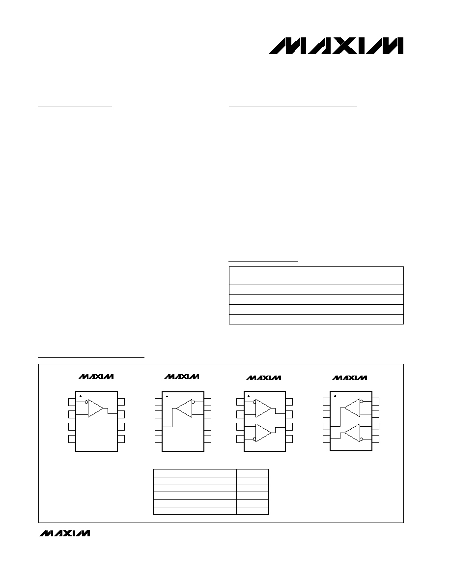
The MAX9111 is a single LVDS receiver, and the
MAX9113 is a dual LVDS receiver.
Both devices conform to the EIA/TIA-644 LVDS standard
and convert LVDS to LVTTL/CMOS-compatible outputs.
A fail-safe feature sets the outputs high when the inputs
are undriven and open, terminated, or shorted. The
MAX9111/MAX9113 are available in space-saving 8-pin
SOT23 and SO packages. Refer to the MAX9110/
MAX9112 data sheet for single/dual LVDS line drivers.
________________________Applications
Features
o Low 300ps (max) Pulse Skew for High-Resolution
Imaging and High-Speed Interconnect
o Space-Saving 8-Pin SOT23 and SO Packages
o Pin-Compatible Upgrades to DS90LV018A and
DS90LV028A (SO Packages Only)
o Guaranteed 500Mbps Data Rate
o Low 29mW Power Dissipation at 3.3V
o Conform to EIA/TIA-644 Standard
o Single +3.3V Supply
o Flow-Through Pinout Simplifies PC Board Layout
o Fail-Safe Circuit Sets Output High for Undriven
Inputs
o High-Impedance LVDS Inputs when Powered Off
MAX9111/MAX9113
Single/Dual LVDS Line Receivers with
Ultra-Low Pulse Skew in SOT23
________________________________________________________________ Maxim Integrated Products
1
OUT2
GND
OUT1
V
CC
IN2+
IN2-
8
7
IN1-
IN1+
6
5
N.C.
GND
N.C.
1
2
8
7
V
CC
OUT
IN+
N.C.
IN-
SO
3
4
6
5
OUT2
GND
IN2-
1
2
8
7
V
CC
OUT1
IN1+
IN2+
IN1-
SO
3
4
6
5
MAX9113
MAX9113
MAX9111
1
2
8
7
N.C.
IN+
N.C.
IN-
SOT23
SOT23
3
4
6
5
OUT
N.C.
V
CC
GND
1
2
3
4
MAX9111
MAX9111
H = LOGIC LEVEL HIGH
L = LOGIC LEVEL LOW
(IN_+) - (IN_-)
100mV
-100mV
OUT_
H
L
H
H
H
OPEN
SHORT
100
PARALLEL TERMINATION (UNDRIVEN)
Pin Configurations/Functional Diagrams/Truth Table
19-4802; Rev 0; 7/00
For free samples and the latest literature, visit www.maxim-ic.com or phone 1-800-998-8800.
For small orders, phone 1-800-835-8769.
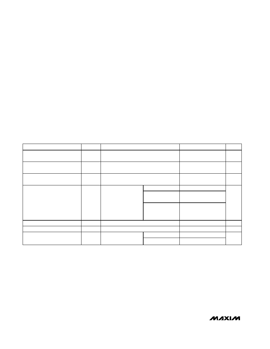
Ordering Information
PART
TEMP.
RANGE
PIN-
PACKAGE
TOP
MARK
MAX9111EKA
-40
°C to +85°C
8 SOT23
AAEE
MAX9111ESA
-40
°C to +85°C
8 SO
--
MAX9113EKA
-40
°C to +85°C
8 SOT23
AAED
MAX9113ESA
-40
°C to +85°C
8 SO
--
Laser Printers
Digital Copiers
Cellular Phone
Base Stations
Telecom Switching
Equipment
Network Switches/Routers
LCD Displays
Backplane Interconnect
Clock Distribution
Typical Operating Circuit appears at end of data sheet.
MAX9111/MAX9113
Single/Dual LVDS Line Receivers with
Ultra-Low Pulse Skew in SOT23
2
_______________________________________________________________________________________
ABSOLUTE MAXIMUM RATINGS
ELECTRICAL CHARACTERISTICS
(V
CC
= +3.0V to +3.6V, magnitude of input voltage, |V
ID
| = +0.1V to +1.0V, V
CM
= |V
ID
|/2 to (2.4V - (|V
ID
|/2)), T
A
= -40°C to +85°C.
Typical values are at V
CC
= +3.3V and T
A
= +25°C, unless otherwise noted.) (Notes 1, 2)
Stresses beyond those listed under "Absolute Maximum Ratings" may cause permanent damage to the device. These are stress ratings only, and functional
operation of the device at these or any other conditions beyond those indicated in the operational sections of the specifications is not implied. Exposure to
absolute maximum rating conditions for extended periods may affect device reliability.
V
CC
to GND ..............................................................-0.3V to +4V
IN_ _ to GND .........................................................-0.3V to +3.9V
OUT_ _ to GND...........................................-0.3V to (V
CC
+ 0.3V)
ESD Protection All Pins
(Human Body Model, IN_+, IN_-) ..................................±11kV
Continuous Power Dissipation (T
A
= +70°C)
8-Pin SOT23 (derate 7.52mW/°C above +70°C)..........602mW
8-Pin SO (derate 5.88mW°C above +70°C).................471mW
Operating Temperature Ranges
MAX911_E .......................................................-40°C to +85°C
Storage Temperature Range .............................-65°C to +150°C
Lead Temperature (soldering, 10s) .................................+300°C
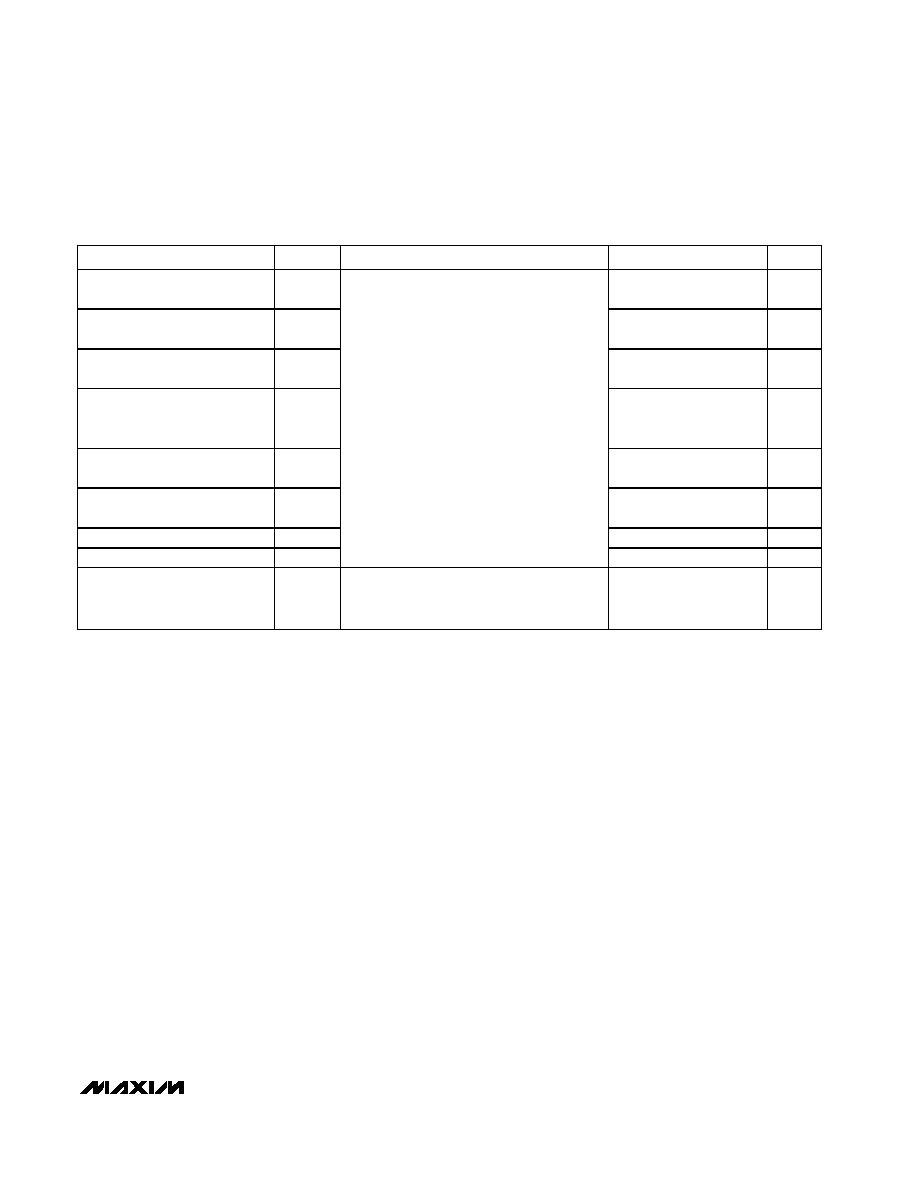
PARAMETER
SYMBOL
CONDITIONS
MIN
TYP
MAX
UNITS
Differential Input High Threshold
(Note 3)
V
TH
V
CM
= 0.05V, 1.2V, 2.75V at 3.3V
100
mV
Differential Input Low Threshold
(Note 3)
V
TL
V
CM
= 0.05V, 1.2V, 2.75V at 3.3V
-100
mV
Differential Input Resistance
R
DIFF
V
CM
= 0.2V or 2.2V, V
ID
= ±0.4V,
V
CC
= 0 or 3.6V
5
18
k
V
ID
= +200mV
2.7
Inputs shorted,
undriven
2.7
Output High Voltage (OUT_)
V
OH
I
OH
= -4mA
100
parallel
termination,
undriven
2.7
V
Output Low Voltage (OUT_)
V
OL
I
OL
= 4mA, V
ID
= -200mV
0.4
Output Short-Circuit Current
I
OS
V
ID
= +200mV, V
OUT
_ = 0
-100
mA
MAX9111
4.2
6
No-Load Supply Current
I
CC
Inputs open
MAX9113
8.7
11
mA
MAX9111/MAX9113
Single/Dual LVDS Line Receivers with
Ultra-Low Pulse Skew in SOT23
_______________________________________________________________________________________
3
SWITCHING CHARACTERISTICS
(V
CC
= +3.0V to +3.6V, T
A
= -40°C to +85°C. Typical values are at V
CC
= +3.3V and T
A
= +25°C, unless otherwise noted.) (Notes 4, 5, 6)
Note 1: Maximum and minimum limits over temperature are guaranteed by design and characterization. Devices are production
tested at
T
A
= +25°C.
Note 2: Current into the device is defined as positive. Current out of the devices is defined as negative. All voltages are referenced
to ground except V
TH
and V
TL
.
Note 3: Guaranteed by design, not production tested.
Note 4: AC parameters are guaranteed by design and characterization.
Note 5: C
L
includes probe and test jig capacitance.
Note 6: f
MAX
generator output conditions: t
R
= t
F
< 1ns (0% to 100%), 50% duty cycle, V
OH
= 1.3V, V
OL
= 1.1V.
Note 7: t
SKD1
is the magnitude difference of differential propagation delays in a channel. t
SKD1
= |t
PLHD
- t
PHLD
|.
Note 8: t
SKD2
is the magnitude difference of the t
PLHD
or t
PHLD
of one channel and the t
PLHD
or t
PHLD
of the other channel on the
same device.
Note 9: t
SKD3
is the magnitude difference of any differential propagation delays between devices at the same V
CC
and within 5
°C
of each other.
Note 10: t
SKD4
, is the magnitude difference of any differential propagation delays between devices operating over the rated supply
and temperature ranges.
PARAMETER
SYMBOL
CONDITIONS
MIN
TYP
MAX
UNITS
Differential Propagation Delay
High to Low
t
PHLD
1
1.77
2.5
ns
Differential Propagation Delay
Low to High
t
PLHD
1
1.68
2.5
ns
Differential Pulse Skew
|t
PLHD
t
PHLD
| (Note 7)
t
SKD1
90
300
ps
Differential Channel-to-Channel
Skew; Same Device
(MAX9113 only) (Note 8)
t
SKD2
140
400
ps
Differential Part-to-Part Skew
(Note 9)
t
SKD3
1
ns
Differential Part-to-Part Skew
(MAX9113 only) (Note 10)
t
SKD4
1.5
ns
Rise Time
t
TLH
0.6
0.8
ns
Fall Time
t
THL
C
L
= 15pF, V
ID
=
±200mV, V
CM
= 1.2V,
Figures 1, 2
0.6
0.8
ns
Maximum Operating Frequency
f
MAX
All channels switching, C
L
=15pF,
V
OL
(max) = 0.4V, V
OH
(min) = 2.7V,
40% < duty cycle < 60% (Note 6)
250
300
MHz
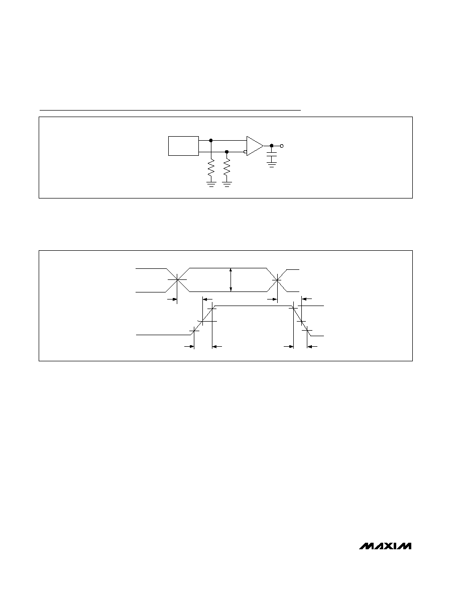
Test Circuit Diagrams
MAX9111/MAX9113
Single/Dual LVDS Line Receivers with
Ultra-Low Pulse Skew in SOT23
4
_______________________________________________________________________________________
C
L
GENERATOR
OUT_
R
IN_+
IN_-
50
50
V
OH
V
OL
IN_-
IN_+
OUT_
t
PHLD
+1.2V
t
THL
20%
80%
80%
50%
50%
t
TLH
20%
DIFFERENTIAL
0V
t
PLHD
V
ID
= 200mV
+1.1V
+1.3V
Figure 1. Receiver Propagation Delay and Transition Time Test Circuit
Figure 2. Receiver Propagation Delay and Transition Time Waveforms
MAX9111/MAX9113
Single/Dual LVDS Line Receivers with
Ultra-Low Pulse Skew in SOT23
_______________________________________________________________________________________
5
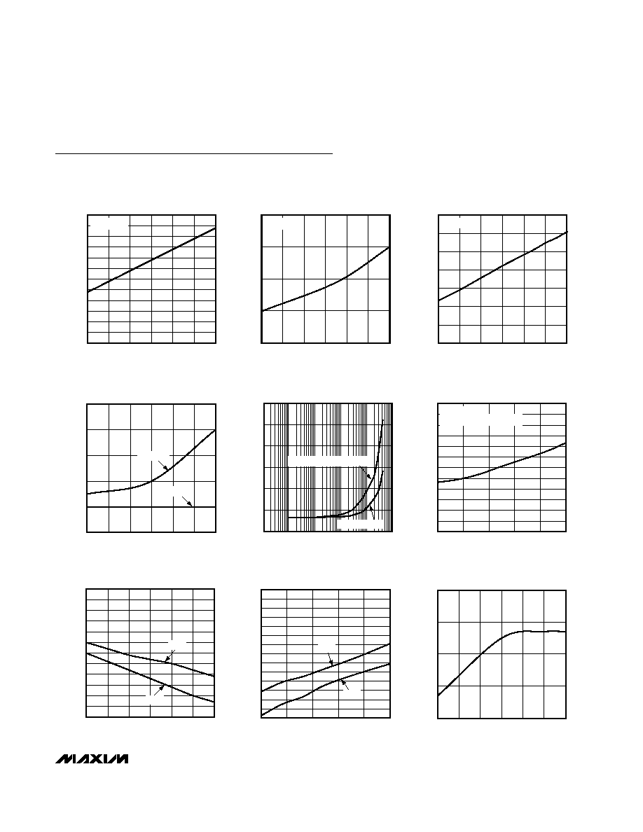
Typical Operating Characteristics
(V
CC
= 3.3V, |V
ID
| = 200mV, V
CM
= 1.2V, f
IN
= 200MHz, C
L
= 15pF, T
A
= +25°C and over recommended operating conditions unless
otherwise specified.)
3.0
3.2
3.1
3.3
3.4
3.5
3.6
MAX9111 toc01
SUPPLY VOLTAGE (V)
OUTPUT HIGH VOLTAGE (V)
OUTPUT HIGH VOLTAGE
vs. SUPPLY VOLTAGE
2.5
2.7
2.6
2.8
2.9
3.0
3.1
3.2
3.3
3.4
3.5
3.6
3.7
I
OUT_
= 4mA
3.0
3.2
3.3
3.1
3.4
3.5
3.6
MAX9111 toc02
SUPPLY VOLTAGE (V)
OUTPUT LOW VOLTAGE (mV)
OUTPUT LOW VOLTAGE
vs. SUPPLY VOLTAGE
130
120
110
100
90
I
OUT_
= 4mA
48
58
53
68
63
78
73
83
3.0
3.2
3.3
3.1
3.4
3.5
3.6
MAX9111 toc03
SUPPLY VOLTAGE (V)
OUTPUT SHORT-CIRCUIT CURRENT (mA)
OUTPUT SHORT-CIRCUIT CURRENT
vs. SUPPLY VOLTAGE
V
ID
= 200mV
14
16
20
18
22
24
3.0
3.2
3.1
3.3
3.4
3.5
3.6
MAX9111 toc04
SUPPLY VOLTAGE (V)
DIFFERENTIAL THRESHOLD VOLTAGE (mV)
DIFFERENTIAL THRESHOLD VOLTAGE
vs. SUPPLY VOLTAGE
HIGH-LOW
LOW-HIGH
0.01
0.1
1
10
100
1000
MAX9111 toc05
FREQUENCY (MHz)
POWER-SUPPLY CURRENT (mA)
0
20
10
40
30
50
60
BOTH CHANNELS SWITCHING
ONE SWITCHING
MAX9113 POWER-SUPPLY CURRENT
vs. FREQUENCY
-40
10
-15
35
60
85
MAX9111 toc06
TEMPERATURE (
°C)
POWER-SUPPLY CURRENT (mA)
POWER-SUPPLY CURRENT
vs. TEMPERATURE
6.5
6.7
6.6
6.8
6.9
7.0
7.1
7.2
7.3
7.4
7.5
7.6
7.7
f
IN
= 1MHz
BOTH CHANNELS SWITCHING
1.50
1.60
1.55
1.65
1.70
1.75
1.80
1.85
1.90
1.95
2.00
2.05
2.10
3.0
3.1
3.2
3.4
3.3
3.5
3.6
DIFFERENTIAL PROPAGATION DELAY
vs. SUPPLY VOLTAGE
MAX9111 toc07
SUPPLY VOLTAGE (V)
DIFFERENTIAL PROPAGATION DELAY (ns)
t
PHLD
t
PLHD
1.50
1.60
1.55
1.65
1.75
1.70
1.80
1.85
1.90
2.00
1.95
2.05
2.10
2.15
2.20
-40
-15
10
35
60
85
DIFFERENTIAL PROPAGATION DELAY
vs. TEMPERATURE
MAX9111 toc08
TEMPERATURE (
°C)
DIFFERENTIAL PROPAGATION DELAY (ns)
t
PHLD
t
PLHD
120
100
80
60
40
3.0
3.3
3.1
3.2
3.4
3.5
3.6
DIFFERENTIAL PULSE SKEW
vs. SUPPLY VOLTAGE
MAX9111 toc09
SUPPLY VOLTAGE (V)
DIFFERENTIAL SKEW (ns)