 | –≠–ª–µ–∫—Ç—Ä–æ–Ω–Ω—ã–π –∫–æ–º–ø–æ–Ω–µ–Ω—Ç: MAX912 | –°–∫–∞—á–∞—Ç—å:  PDF PDF  ZIP ZIP |

_______________General Description
The MAX913 single and MAX912 dual high-speed,
low-power comparators have differential inputs and
complementary TTL outputs. Fast propagation delay
(10ns typ), extremely low supply current, and a wide
common-mode input range that includes the negative
rail make the MAX912/MAX913 ideal for low-power,
high-speed, single +5V (or ±5V) applications such as
V/F converters or switching regulators.
The MAX912/MAX913 outputs remain stable through
the linear region. This feature eliminates output instability
common to high-speed comparators when driven with a
slow-moving input signal.
The MAX912/MAX913 can be powered from a single
+5V supply or a ±5V split supply. The MAX913 is an
improved plug-in replacement for the LT1016. It pro-
vides significantly wider input voltage range
and
equiva-
lent speed at a fraction of the power. The MAX912 dual
comparator has equal performance to the MAX913 and
includes independent latch controls.
________________________Applications
Zero-Crossing Detectors
Ethernet Line Receivers
Switching Regulators
High-Speed Sampling Circuits
High-Speed Triggers
Extended Range V/F Converters
Fast Pulse Width/Height Discriminators
____________________________Features
o
Ultra Fast (10ns)
o
Single +5V or Dual ±5V Supply Operation
o
Input Range Extends Below Negative Supply
o
Low Power: 6mA (+5V) Per Comparator
o
No Minimum Input Signal Slew-Rate Requirement
o
No Power-Supply Current Spiking
o
Stable in the Linear Region
o
Inputs Can Exceed Either Supply
o
Low Offset Voltage: 0.8mV
______________Ordering Information
* Dice are specified at T
A
= +25 ∞C, DC parameters only.
MAX912/MAX913
Single/Dual, Ultra-Fast, Low-Power,
Precision TTL Comparators
________________________________________________________________
Maxim Integrated Products
1
1
2
3
4
8
7
6
5
V+
IN+
IN-
V-
Q
Q
GND
LE
DIP/SO
MAX913
+
-
TOP VIEW
___________________________________________________________Pin Configurations
Call toll free 1-800-998-8800 for free samples or literature.
19-0157; Rev 1; 1/94
PART
TEMP. RANGE
PIN-PACKAGE
MAX912
CPE
0∞C to +70∞C
16 Plastic DIP
MAX912CSE
0∞C to +70∞C
16 Narrow SO
MAX912C/D
0∞C to +70∞C
Dice*
MAX912EPE
-40∞C to +85∞C
16 Plastic DIP
MAX912ESE
-40∞C to +85∞C
16 Narrow SO
MAX912MJE
-55∞C to +125∞C
16 CERDIP
N.C.
V-
INA-
LEB
N.C.
V+
INB-
DIP/Narrow SO
1
16
QA
GND
LEA
QB
GND
MAX912
8
9
INA+
INB+
+
-
QA
QB
+
-
A
B
4
5
6
7
13
12
11
10
2
3
15
14
MAX913
CPA
0∞C to +70∞C
8 Plastic DIP
MAX913CSA
0∞C to +70∞C
8 SO
MAX913C/D
0∞C to +70∞C
Dice*
MAX913EPA
-40∞C to +85∞C
8 Plastic DIP
MAX913ESA
-40∞C to +85∞C
8 SO
MAX913MJA
-55∞C to +125∞C
8 CERDIP
MAX912/MAX913
Single/Dual, Ultra-Fast, Low-Power,
Precision TTL Comparators
2
_______________________________________________________________________________________
ABSOLUTE MAXIMUM RATINGS
Positive Supply Voltage............................................................7V
Negative Supply Voltage ........................................................-7V
Differential Input Voltage .....................................................±15V
Input Voltage (Referred to V-)..................................- 0.3V to 15V
Latch Pin Voltage .............................................Equal to Supplies
Continuous Output Current...............................................±20mA
Continuous Power Dissipation (T
A
= +70∞C)
8-Pin Plastic DIP (derate 9.09mW/∞C above +70∞C) ...727mW
8-Pin SO (derate 5.88mW/∞C above +70∞C)................471mW
8-Pin CERDIP (derate 8.00mW/∞C above +70∞C)........640mW
16-Pin Plastic DIP (derate 10.53mW/∞C above +70∞C)...842mW
16-Pin Narrow SO (derate 8.70mW/∞C above +70∞C) ...696mW
16-Pin CERDIP (derate 10.00mW/∞C above +70∞C)....800mW
Operating Temperature Ranges:
MAX91_ C_ _ ......................................................0∞C to +70∞C
MAX91_ E_ _....................................................-40∞C to +85∞C
MAX91_ MJ_ .................................................-55∞C to +125∞C
Storage Temperature Range .............................-65∞C to +150∞C
Lead Temperature (soldering, 10sec) .............................+300∞C
Stresses beyond those listed under "Absolute Maximum Ratings" may cause permanent damage to the device. These are stress ratings only, and functional
operation of the device at these or any other conditions beyond those indicated in the operational sections of the specifications is not implied. Exposure to
absolute maximum rating conditions for extended periods may affect device reliability.
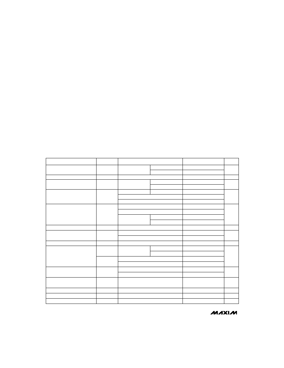
PARAMETER
R
S
100
SYMBOL
MIN
TYP
MAX
T
A
= T
MIN
to T
MAX
UNITS
T
A
= +25∞C
3
T
A
= T
MIN
to T
MAX
Offset Drift
TCV
OS
2
µV/∞C
Input Offset Current (Note 1)
I
OS
0.3
0.5
µA
T
A
= +25∞C
0.8
T
A
= +25∞C
Input Bias Current
I
B
3
5
µA
C, E temp. ranges
8
M temp. range
10
CONDITIONS
Input Offset Voltage (Note 1)
V
OS
0.8
2
mV
Single +5V
C, E temp. ranges
Power-Supply Rejection Ratio
PSRR
M temp. range
Positive supply: 4.5V
V+
5.5V
60
85
M temp. range
-5.0
+3.5
-5.0V
V
CM
+3.5V
dB
I
OUT
= 1mA
V
OL
-0.2
+3.5
Negative supply: -2V
V-
-7V
Common-Mode Rejection Ratio
CMRR
80
100
0
+3.5
dB
C, E temp. ranges
I
OUT
= 10mA
80
110
Small-Signal Voltage Gain
A
V
1V
V
Q
2V, T
A
= +25∞C
1500
3500
V/V
Output Voltage
V
OH
V+
4.5V
2.7
3.4
V
2.4
3.0
I
SINK
= 4mA
0.3
0.5
T
A
= +25∞C, I
SINK
= 10mA
0.4
Input Voltage Range
V
CM
-5.2
+3.5
V
ELECTRICAL CHARACTERISTICS
(V+ = +5V, V- = -5V, V
Q
= 1.4V, V
LE
= 0V, T
A
= T
MIN
to T
MAX
, unless otherwise noted. Typical values are at T
A
= +25∞C.)
12
C, E temp. ranges
6
10
Positive Supply Current Per
Comparator
I+
M temp. range
12
mA
Latch-Pin High Input Voltage
V
IH
I-
0.4
2
mA
2.0
V
Latch-Pin Current
I
IL
V
LE
= 0V
Latch-Pin Low Input Voltage
V
IL
0.8
V
-20
µA
Negative Supply Current Per
Comparator
MAX912/MAX913
Single/Dual, Ultra-Fast, Low-Power,
Precision TTL Comparators
_______________________________________________________________________________________
3
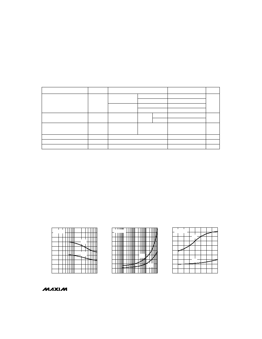
ELECTRICAL CHARACTERISTICS (continued)
(V+ = +5V, V- = -5V, V
Q
= 1.4V, V
LE
= 0V, T
A
= T
MIN
to T
MAX
, unless otherwise noted).
T
A
= +25∞C
T
A
= T
MIN
to T
MAX
V
IN
= 100mV,
V
OD
= 20mV
9
12
T
A
= +25∞C
Propagation Delay (Note 2)
t
PD+
, t
PD-
V
IN
= 100mV,
V
OD
= 5mV
10
14
ns
16
15
T
A
= T
MIN
to T
MAX
Note 1:
Input Offset Voltage (V
OS
) is defined as the average of the two input offset voltages, measured by forcing first one output,
then the other to 1.4V. Input Offset Current (I
OS
) is defined the same way.
Note 2:
Propagation Delay (t
PD
) and Differential Propagation Delay (
t
PD
) cannot be measured in automatic handling equipment
with low input overdrive values. The MAX912/MAX913 are sample tested to 0.1% AQL with a 1V step and 500mV overdrive
at +25∞C only. Correlation tests show that t
PD
and
t
PD
can be guaranteed with this test, if additional DC tests are per-
formed to guarantee that all internal bias conditions are correct. For low overdrive conditions, V
OS
is added to the over-
drive. Differential Propagation Delay is defined as:
t
PD
= t
PD+
≠ t
PD
-.
Note 3:
Input latch setup time (t
SU
) is the interval in which the input signal must be stable prior to asserting the latch signal.
The hold time (t
H
) is the interval after the latch is asserted in which the input signal must be stable. These parameters are
guaranteed by design.
Note 4:
Latch Propagation Delay (t
LPD
) is the delay time for the output to respond when the latch-enable pin is deasserted.
See Timing Diagram.
CONDITIONS
PARAMETER
SYMBOL
UNITS
MIN
TYP
MAX
T
A
=
+25∞C
V
IN
= 100mV,
V
OD
= 5mV
2
3
ns
2
0
t
SU
t
PD
Latch Setup Time (Note 3)
ns
Differential Propagation Delay
(Note 2)
T
A
= +25∞C
V
IN
= 100mV,
V
OD
= 5mV
(MAX912 only)
500
ps
Channel-to-Channel
Propagation Delay
(Note 2)
3
2
t
H
Latch Hold Time (Note 3)
ns
7
t
LPD
Latch Propagation Delay (Note 4)
ns
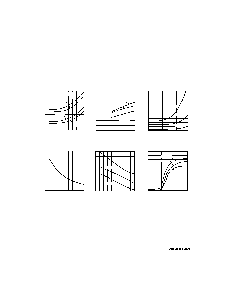
__________________________________________Typical Operating Characteristics
(V+ = 5V, V- = -5V, V
LE
= 0V, C
L
= 15pF, T
A
= +25∞C, unless otherwise noted.)
5
1
10
100
PROPAGATION DELAY
vs. INPUT OVERDRIVE
INPUT OVERDRIVE (mV)
PROPAGATION DELAY (ns)
6
7
8
9
10
t
PD(-)
t
PD(+)
MAX912-01
V
OD
= 10mV
50
0
1
100
10,000
PROPAGATION DELAY
vs. SOURCE RESISTANCE
10
MAX912-02
SOURCE RESISTANCE (
)
PROPAGATION DEALY (ns)
20
30
40
10
1000
t
PD(-)
t
PD(+)
V
OD
= 10mV
PROPAGATION DELAY
vs. LOAD CAPACITANCE
PROPAGATION DELAY (ns)
6
10
20
30
40
50
LOAD CAPACITANCE (pF)
MAX912-03
7
8
9
10
11
t
PD(-)
t
PD(+)
V
OD
= 10mV
MAX913
3
5
MAX912
MAX912/MAX913
Single/Dual, Ultra-Fast, Low-Power,
Precision TTL Comparators
4
_______________________________________________________________________________________
____________________________Typical Operating Characteristics (continued)
(V+ = 5V, V- = -5V, V
LE
= 0V, C
L
= 15pF, T
A
= +25∞C, unless otherwise noted.)
PROPAGATION DELAY
vs. TEMPERATURE
PROPAGATION DELAY (ns)
TEMPERATURE (∞C)
6
-55
MAX912-04
-15
25
105 125
65
7
8
9
10
11
Q OUTPUT
t
PD(-)
Q OUTPUT
t
PD(-)
Q OUTPUT
t
PD(+)
Q OUTPUT
t
PD(+)
V
OD
= 10mV
POSITIVE SUPPLY CURRENT
(PER COMPARATOR)
vs. POSTIVE SUPPLY VOLTAGE
I+ (PER COMPARATOR)
2
4
6
8
10
3
4
5
6
7
V+ (V)
MAX912-07
T
A
= +125∞C
T
A
= +25∞C
T
A
= -55∞C
V- = 0V TO -5V
NEGATIVE SUPPLY CURRENT
(PER COMPARATOR)
vs. NEGATIVE SUPPLY VOLTAGE
I- (PER COMPARATOR)
V- (V)
0.2
0
MAX912-08
1
2
3
4
5
6
7
0.4
0.6
0.8
1.0
1.2
T
A
= +125∞C
T
A
= +25∞C
T
A
= -55∞C
OFFSET VOLTAGE
vs. TEMPERATURE
V
OS
(
µ
V)
0
-55
TEMPERATURE (∞C)
MAX912-11
-15
25
65
105 125
200
400
800
1000
600
INPUT BIAS CURRENT
vs. TEMPERATURE
I
B
(
µ
A)
2
TEMPERATURE (∞C)
MA912-12
-55
-15
25
65
105 125
3
4
5
6
V
CM
= -5.2V
V
CM
= 0V
V
CM
= +3.5V
OUTPUT VOLTAGE
vs. DIFFERENTIAL INPUT VOLTAGE
OUTPUT VOLTAGE (V)
DIFFERENTIAL INPUT VOLTAGE (mV)
0
-3
MAX912-14
-2
-1
1
2
3
0
1
2
3
4
5
T
A
= +125∞C
T
A
= +25∞C
T
A
= -55∞C

MAX912/MAX913
Single/Dual, Ultra-Fast, Low-Power,
Precision TTL Comparators
_______________________________________________________________________________________
5
____________________________Typical Operating Characteristics (continued)
(V+ = 5V, V- = -5V, V
LE
= 0V, C
L
= 15pF, T
A
= +25∞C, unless otherwise noted.)
POSITIVE-TO-NEGATIVE PROPAGATION DELAY
INPUT
100mV/div
OUTPUT
Q
1V/div
Q
5ns/div
NEGATIVE-TO-POSITIVE PROPAGATION DELAY
INPUT
100mV/div
OUTPUT
Q
1V/div
Q
5ns/div
MAX912/MAX913 RESPONSE TO
50MHz (
+
10mV
P-P
) SINE WAVE
INPUT
10mV/div
OUTPUT
Q
2V/div
10ns/div
INDUSTRY STANDARD
686 RESPONSE
INPUT
20mV/div
OUTPUT
Q
1V/div
Q
20
µ
s/div
1V/div
MAX912/MAX913 RESPONSE
INPUT
20mV/div
OUTPUT
Q
1V/div
Q
20
µ
s/div
1V/div
MAX912/MAX913 RESPONSE TO SLOW-MOVING TRIANGLE WAVE