 | ÐлекÑÑоннÑй компоненÑ: MAX9120 | СкаÑаÑÑ:  PDF PDF  ZIP ZIP |
Äîêóìåíòàöèÿ è îïèñàíèÿ www.docs.chipfind.ru
General Description
The MAX9117MAX9120 nanopower comparators in
space-saving SC70 packages feature Beyond-the-
RailsTM inputs and are guaranteed to operate down to
+1.8V. The MAX9117/MAX9118 feature an on-board
1.252V ±1.75% reference and draw an ultra-low supply
current of only 600nA, while the MAX9119/MAX9120
(without reference) require just 350nA of supply current.
These features make the MAX9117MAX9120 family of
comparators ideal for all 2-cell battery-monitoring/man-
agement applications.
The unique design of the output stage limits supply-cur-
rent surges while switching, virtually eliminating the sup-
ply glitches typical of many other comparators. This
design also minimizes overall power consumption under
dynamic conditions. The MAX9117/MAX9119 have a
push-pull output stage that sinks and sources current.
Large internal-output drivers allow Rail-to-Rail
®
output
swing with loads up to 5mA. The MAX9118/MAX9120
have an open-drain output stage that makes them suit-
able for mixed-voltage system design. All devices are
available in the ultra-small 5-pin SC70 package.
Applications
2-Cell Battery Monitoring/Management
Ultra-Low-Power Systems
Mobile Communications
Notebooks and PDAs
Threshold Detectors/Discriminators
Sensing at Ground or Supply Line
Telemetry and Remote Systems
Medical Instruments
Features
o Space-Saving SC70 Package (Half the Size of
SOT23)
o Ultra-Low Supply Current
350nA Per Comparator (MAX9119/MAX9120)
600nA Per Comparator with Reference
(MAX9117/MAX9118)
o Guaranteed to Operate Down to +1.8V
o Internal 1.252V ±1.75% Reference
(MAX9117/MAX9118)
o Input Voltage Range Extends 200mV
Beyond-the-Rails
o CMOS Push-Pull Output with ±5mA Drive
Capability (MAX9117/MAX9119)
o Open-Drain Output Versions Available
(MAX9118/MAX9120)
o Crowbar-Current-Free Switching
o Internal Hysteresis for Clean Switching
o No Phase Reversal for Overdriven Inputs
MAX9117MAX9120
SC70, 1.8V, Nanopower, Beyond-the-Rails
Comparators With/Without Reference
________________________________________________________________ Maxim Integrated Products
1
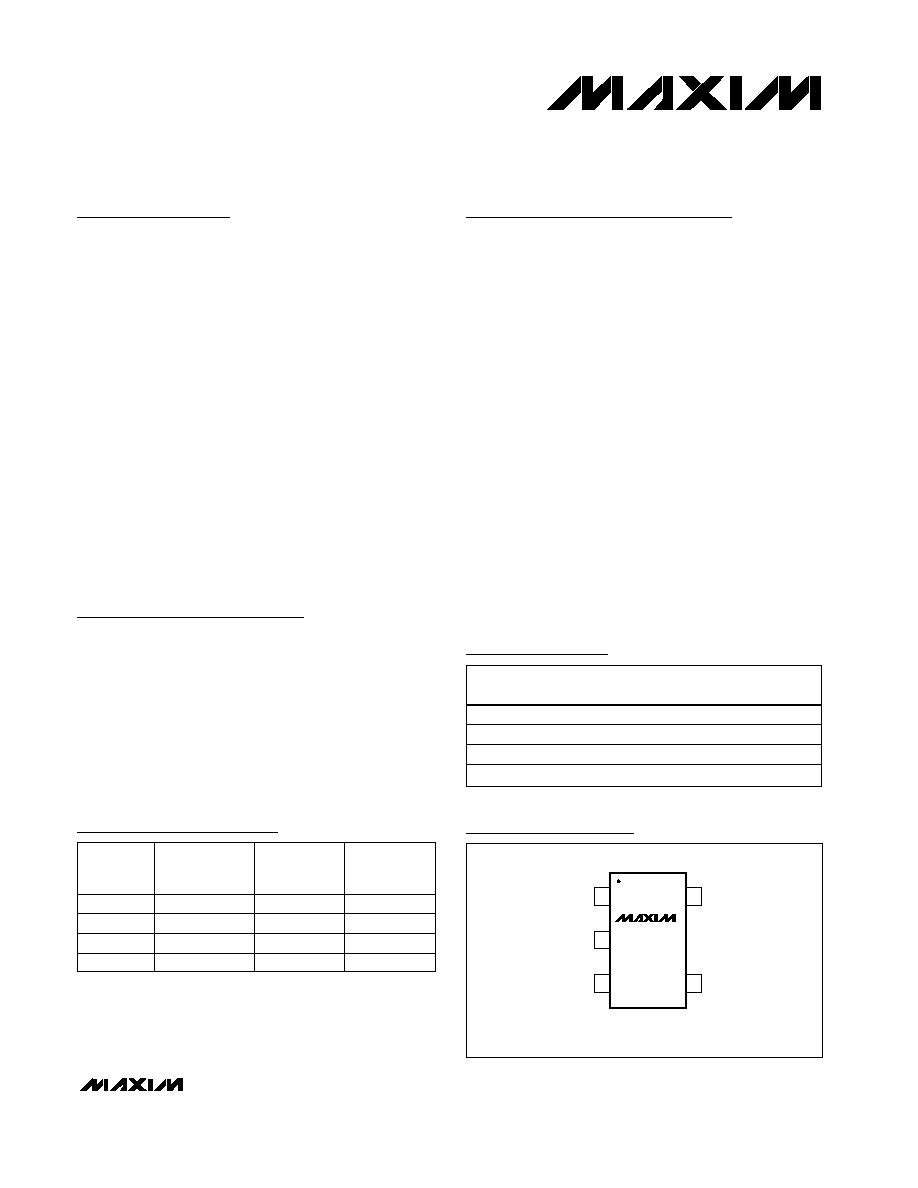
V
EE
IN- (REF)
IN+
1
5
V
CC
OUT
MAX9117
MAX9118
MAX9119
MAX9120
SC70
TOP VIEW
2
3
4
( ) ARE FOR MAX9117/MAX9118.
Typical Application Circuit appears at end of data sheet.
Pin Configurations
Selector Guide
Ordering Information
Beyond-the-Rails is a trademark of Maxim Integrated Products, Inc.
Rail-to-Rail is a registered trademark of Nippon Motorola, Ltd.
19-1862; Rev 2; 8/02
PART
INTERNAL
REFERENCE
OUTPUT
TYPE
SUPPLY
CURRENT
(nA)
MAX9117
Yes
Push-Pull
600
MAX9118
Yes
Open-Drain
600
350
Push-Pull
No
MAX9119
MAX9120
No
Open-Drain
350
PART
TEMP
RANGE
PIN-
PACKAGE
TOP
MARK
MAX9117EXK-T
-40
°C to +85°C 5 SC70-5
ABW
MAX9118EXK-T
-40
°C to +85°C 5 SC70-5
ABX
MAX9119EXK-T
-40
°C to +85°C 5 SC70-5
ABY
MAX9120EXK-T
-40
°C to +85°C 5 SC70-5
ABZ
For pricing, delivery, and ordering information, please contact Maxim/Dallas Direct! at
1-888-629-4642, or visit Maxim's website at www.maxim-ic.com.
MAX9117MAX9120
SC70, 1.8V, Nanopower, Beyond-the-Rails
Comparators With/Without Reference
2
_______________________________________________________________________________________
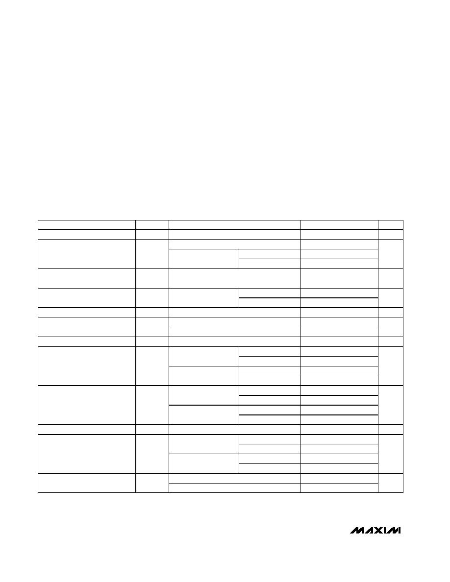
ABSOLUTE MAXIMUM RATINGS
ELECTRICAL CHARACTERISTICS--MAX9117/MAX9118
(V
CC
= +5V, V
EE
= 0V, V
IN+
= V
REF
, T
A
= -40°C to +85°C, unless otherwise noted. Typical values are at T
A
= +25°C.) (Note 1)
Stresses beyond those listed under "Absolute Maximum Ratings" may cause permanent damage to the device. These are stress ratings only, and functional
operation of the device at these or any other conditions beyond those indicated in the operational sections of the specifications is not implied. Exposure to
absolute maximum rating conditions for extended periods may affect device reliability.
Supply Voltage (V
CC
to V
EE
)..................................................+6V
Voltage Inputs (IN+, IN-, REF) .........(V
EE
- 0.3V) to (V
CC
+ 0.3V)
Output Voltage
MAX9117/MAX9119 ....................(V
EE
- 0.3V) to (V
CC
+ 0.3V)
MAX9118/MAX9120 ..................................(V
EE
- 0.3V) to +6V
Current Into Input Pins ........................................................20mA
Output Current..................................................................±50mA
Output Short-Circuit Duration .................................................10s
Continuous Power Dissipation (T
A
= +70°C)
5-Pin SC70 (derate 2.5mW/°C above +70°C) .............200mW
Operating Temperature Range ...........................-40°C to +85°C
Junction Temperature ......................................................+150°C
Storage Temperature Range .............................-65°C to +150°C
Lead Temperature (soldering, 10s) .................................+300°C
PARAMETER
SYMBOL
CONDITIONS
MIN
TYP
MAX
UNITS
Supply Voltage Range
V
CC
Inferred from the PSRR test
1.8
5.5
V
V
CC
= 1.8V
0.60
T
A
= +25°C
0.68
Supply Current
I
CC
V
CC
= 5V
T
A
= T
MIN
to T
MAX
1.30
µA
IN+ Voltage Range
V
IN+
Inferred from output swing test
V
EE
-
0.2
V
CC
+
0.2
V
T
A
= +25°C
1
5
Input Offset Voltage
V
OS
(Note 2)
T
A
= T
MIN
to T
MAX
10
mV
Input-Referred Hysteresis
V
HB
(Note 3)
4
mV
T
A
= +25°C
0.15
1
Input Bias Current
I
B
T
A
= T
MIN
to T
MAX
2
nA
Power-Supply Rejection Ratio
PSRR
V
CC
= 1.8V to 5.5V
0.1
1
mV/V
T
A
= +25°C
190
400
MAX9117, V
CC
= 5V,
I
SOURCE
= 5mA
T
A
= T
MIN
to T
MAX
500
T
A
= +25°C
100
200
Output Voltage Swing High
V
CC
-
V
OH
MAX9117, V
CC
= 1.8V,
I
SOURCE
= 1mA
T
A
= T
MIN
to T
MAX
300
mV
T
A
= +25°C
190
400
V
CC
= 5V, I
SINK
= 5mA
T
A
= T
MIN
to T
MAX
500
T
A
= +25°C
100
200
Output Voltage Swing Low
V
OL
V
CC
= 1.8V, I
SINK
= 1mA
T
A
= T
MIN
to T
MAX
300
mV
Output Leakage Current
I
LEAK
MAX9118 only, V
O
= 5.5V
0.002
1
mA
V
CC
= 5V
35
Sourcing, V
O
= V
EE
V
CC
= 1.8V
3
V
CC
= 5V
35
Output Short-Circuit Current
I
SC
Sinking, V
O
= V
CC
V
CC
= 1.8V
3
mA
V
CC
= 1.8V
16
High-to-Low Propagation Delay
(Note 4)
t
PD
-
V
CC
= 5V
14
µs
MAX9117MAX9120
SC70, 1.8V, Nanopower, Beyond-the-Rails
Comparators With/Without Reference
_______________________________________________________________________________________
3
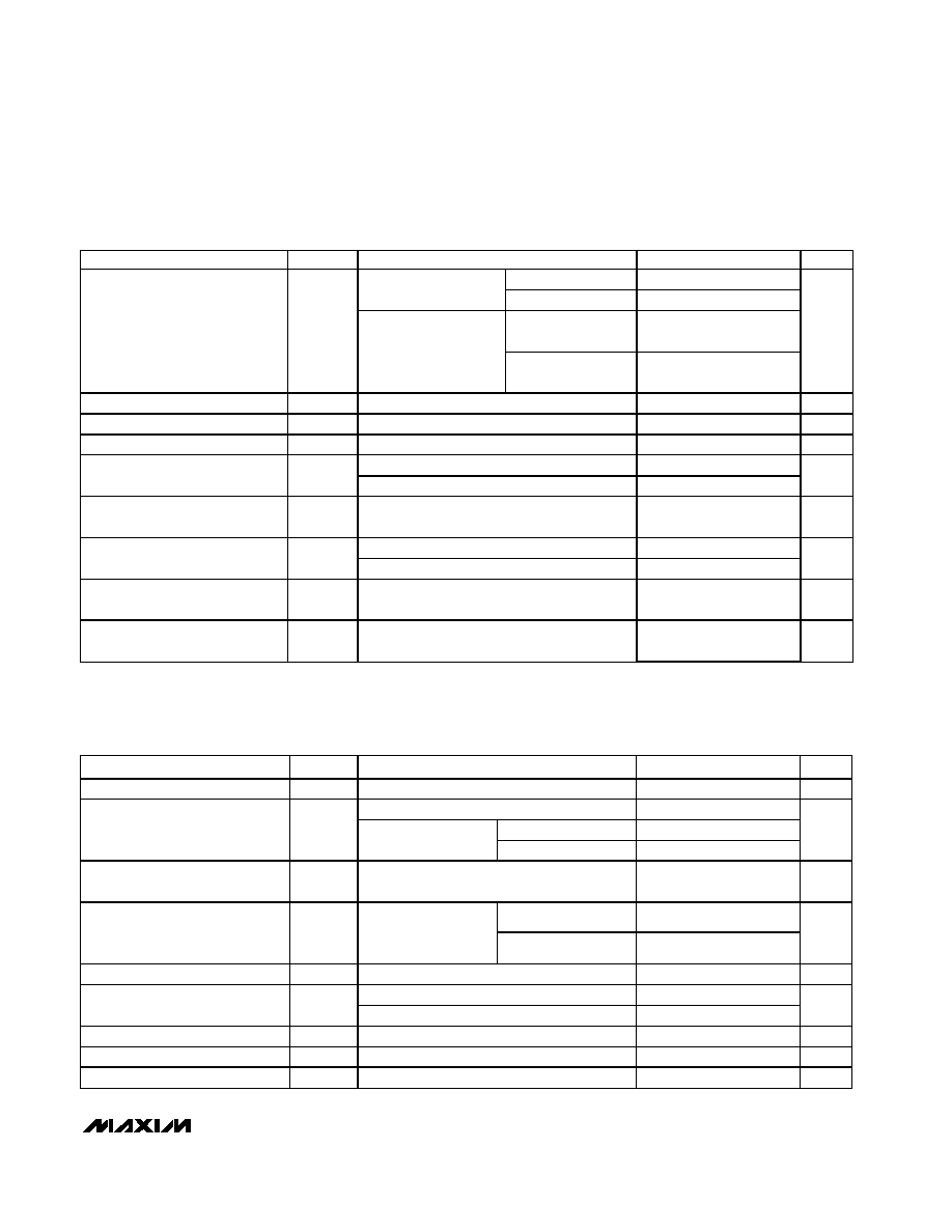
ELECTRICAL CHARACTERISTICS--MAX9119/MAX9120
(V
CC
= +5V, V
EE
= 0V, V
CM
= 0V, T
A
= -40°C to +85°C, unless otherwise noted. Typical values are at T
A
= +25°C.) (Note 1)
ELECTRICAL CHARACTERISTICS--MAX9117/MAX9118 (continued)
(V
CC
= +5V, V
EE
= 0V, V
IN+
= V
REF
, T
A
= -40°C to +85°C, unless otherwise noted. Typical values are at T
A
= +25°C.) (Note 1)
PARAMETER
SYMBOL
CONDITIONS
MIN
TYP
MAX
UNITS
V
CC
= 1.8V
15
MAX9117 only
V
CC
= 5V
40
V
CC
= 1.8V,
R
PULLUP
= 100k
16
Low-to-High Propagation Delay
(Note 4)
t
PD+
MAX9118 only
V
CC
= 5V,
R
PULLUP
= 100k
45
µs
Rise Time
t
RISE
MAX9117 only, C
L
= 15pF
1.6
µs
Fall Time
t
FALL
C
L
= 15pF
0.2
µs
Power-Up Time
t
ON
1.2
ms
T
A
= +25°C
1.230
1.252
1.274
Reference Voltage
V
REF
T
A
= T
MIN
to T
MAX
1.196
1.308
V
Reference Voltage Temperature
Coefficient
TC
REF
100
pp m/
°C
BW = 10Hz to 100kHz
1.1
Reference Output Voltage
Noise
E
N
BW = 10Hz to 100kHz, C
REF
= 1nF
0.2
mV
RMS
Reference Line Regulation
V
REF
/
V
CC
V
CC
= 1.8V to 5.5V
0.25
mV/V
Reference Load Regulation
V
REF
/
I
OUT
I
OUT
= 10nA
±1
mV/
nA
PARAMETER
SYMBOL
CONDITIONS
MIN
TYP
MAX
UNITS
Supply Voltage Range
V
CC
Inferred from the PSRR test
1.8
5.5
V
V
CC
= 1.8V
0.35
T
A
= +25
°C
0.45
0.80
Supply Current
I
CC
V
CC
= 5V
T
A
= T
MIN
to T
MAX
1.2
µA
Input Common-Mode
Voltage Range
V
CM
Inferred from the CMRR test
V
EE
-
0.2
V
CC
+
0.2
V
T
A
= +25
°C
1
5
Input Offset Voltage
V
OS
-0.2V
V
CM
(V
CC
+ 0.2V)
(Note 2)
T
A
= T
MIN
to T
MAX
10
mV
Input-Referred Hysteresis
V
HB
-0.2V
V
CM
(V
CC
+ 0.2V) (Note 3)
4
mV
T
A
= +25
°C
0.15
1
Input Bias Current
I
B
T
A
= T
MIN
to T
MAX
2
nA
Input Offset Current
I
OS
75
pA
Power-Supply Rejection Ratio
PSRR
V
CC
= 1.8V to 5.5V
0.1
1
mV/V
Common-Mode Rejection Ratio
CMRR
(V
EE
- 0.2V)
V
CM
(V
CC
+ 0.2V)
0.5
3
mV/V
MAX9117MAX9120
SC70, 1.8V, Nanopower, Beyond-the-Rails
Comparators With/Without Reference
4
_______________________________________________________________________________________
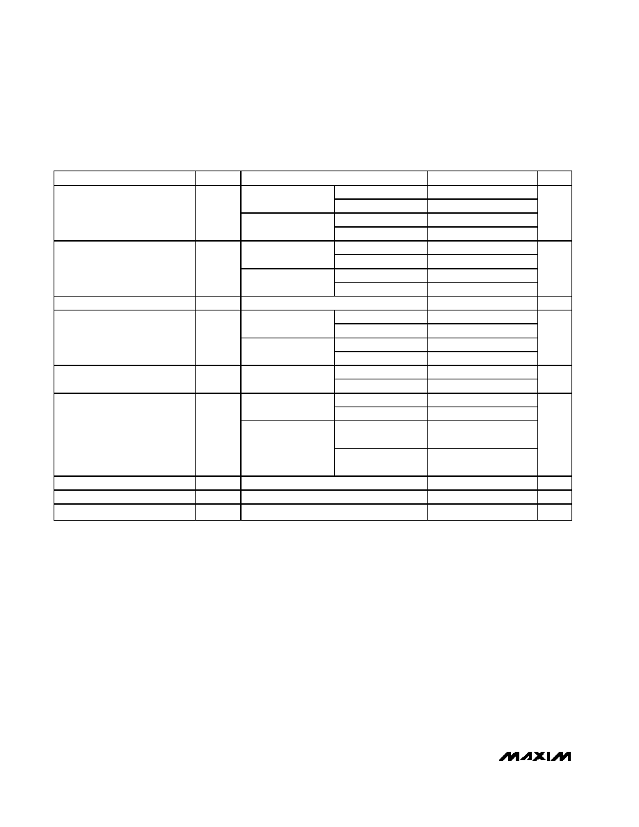
ELECTRICAL CHARACTERISTICS--MAX9119/MAX9120 (continued)
(V
CC
= +5V, V
EE
= 0V, V
CM
= 0V, T
A
= -40°C to +85°C, unless otherwise noted. Typical values are at T
A
= +25°C.) (Note 1)
Note 1: All specifications are 100% tested at T
A
= +25°C. Specification limits over temperature (T
A
= T
MIN
to T
MAX
) are guaranteed
by design, not production tested.
Note 2: V
OS
is defined as the center of the hysteresis band at the input.
Note 3: The hysteresis-related trip points are defined as the edges of the hysteresis band, measured with respect to the center of
the band (i.e., V
OS
) (Figure 2).
Note 4: Specified with an input overdrive (V
OVERDRIVE
) of 100mV, and load capacitance of C
L
= 15pF. V
OVERDRIVE
is defined
above and beyond the offset voltage and hysteresis of the comparator input. For the MAX9117/MAX9118, reference voltage
error should also be added.
PARAMETER
SYMBOL
CONDITIONS
MIN
TYP
MAX
UNITS
T
A
= +25
°C
190
400
MAX9119 only, V
CC
=
5V, I
SOURCE
= 5mA
T
A
= T
MIN
to T
MAX
500
T
A
= +25
°C
100
200
Output Voltage Swing High
V
CC
-
V
OH
MAX9120 only, V
CC
=
1.8V, I
SOURCE
= 1mA
T
A
= T
MIN
to T
MAX
300
mV
T
A
= +25
°C
190
400
V
CC
= 5V,
I
SINK
= 5mA
T
A
= T
MIN
to T
MAX
500
T
A
= +25
°C
100
200
Output Voltage Swing Low
V
OL
V
CC
= 1.8V,
I
SINK
= 1mA
T
A
= T
MIN
to T
MAX
300
mV
Output Leakage Current
I
LEAK
MAX9120 only, V
O
= 5.5V
0.001
1
µA
V
CC
= 5V
35
Sourcing, V
O
= V
EE
V
CC
= 1.8V
3
V
CC
= 5V
35
Output Short-Circuit Current
I
SC
Sourcing, V
O
= V
CC
V
CC
= 1.8V
3
mA
V
CC
= 1.8V
16
High-to-Low Propagation Delay
(Note 4)
t
PD-
V
CC
= 5V
14
µs
V
CC
= 1.8V
15
MAX9119 only
V
CC
= 5V
40
V
CC
= 1.8V,
R
PULLUP
= 100k
16
Low-to-High Propagation Delay
(Note 4)
t
PD+
MAX9120 only
V
CC
= 5V,
R
PULLUP
= 100k
45
µs
Rise Time
t
RISE
MAX9119 only, C
L
= 15pF
1.6
µs
Fall Time
t
FALL
C
L
= 15pF
0.2
µs
Power-Up Time
t
ON
1.2
ms
500
600
550
650
700
750
800
900
850
950
1.5
2.5
2.0
3.0
3.5
4.0
4.5
5.0
5.5
MAX9117/MAX9118 SUPPLY CURRENT
vs. SUPPLY VOLTAGE AND TEMPERATURE
MAX9117-20 toc01
SUPPLY VOLTAGE (V)
SUPPLY CURRENT (nA)
T
A
= +85
°C
T
A
= +25
°C
T
A
= -40
°C
250
300
350
400
450
500
550
1.5
2.5
2.0
3.0
3.5
4.0
4.5
5.0
5.5
MAX9119/MAX9120 SUPPLY CURRENT
vs. SUPPLY VOLTAGE AND TEMPERATURE
MAX9117-20 toc02
SUPPLY VOLTAGE (V)
SUPPLY CURRENT (nA)
T
A
= +85
°C
T
A
= +25
°C
T
A
= -40
°C
550
650
600
750
700
850
800
900
-40
10
-15
35
60
85
MAX9117/MAX9118
SUPPLY CURRENT vs. TEMPERATURE
MAX9117-20 toc03
TEMPERATURE (
°C)
SUPPLY CURRENT (nA)
V
CC
= +3V
V
CC
= +5V
V
CC
= +1.8V
250
350
300
450
400
500
550
-40
10
-15
35
60
85
MAX9119/MAX9120
SUPPLY CURRENT vs. TEMPERATURE
MAX9117-20 toc04
TEMPERATURE (
°C)
SUPPLY CURRENT (nA)
V
CC
= +3V
V
CC
= +5V
V
CC
= +1.8V
0
300
200
100
400
500
600
700
0
2
3
1
4
5
6
9
10
OUTPUT VOLTAGE LOW
vs. SINK CURRENT
MAX9117-20 toc07
SINK CURRENT (mA)
V
OL
(mV)
7
8
V
CC
= +1.8V
V
CC
= +5V
V
CC
= +3V
35
0
1
10
100
1k
10k
100k
MAX9117/MAX9118 SUPPLY CURRENT
vs. OUTPUT TRANSITION FREQUENCY
10
MAX9117-20 toc05
OUTPUT TRANSITION FREQUENCY (Hz)
SUPPLY CURRENT (
µ
A)
25
30
5
15
20
V
CC
= +1.8V
V
CC
= +5V
V
CC
= +3V
35
0
1
10
100
1k
10k
100k
MAX9119/MAX9120 SUPPLY CURRENT
vs. OUTPUT TRANSITION FREQUENCY
10
MAX9117-20 toc06
OUTPUT TRANSITION FREQUENCY (Hz)
SUPPLY CURRENT (
µ
A)
25
30
5
15
20
V
CC
= +1.8V
V
CC
= +5V
V
CC
= +3V
0
100
200
300
400
500
600
0
2
4
6
8
10
OUTPUT VOLTAGE LOW vs. SINK CURRENT
AND TEMPERATURE
MAX9117-20 toc08
SINK CURRENT (mA)
V
OL
(mV)
3
1
5
7
9
T
A
= +85
°C
T
A
= +25
°C
T
A
= -40
°C
0
0.2
0.1
0.4
0.3
0.6
0.5
0.7
0
4
2
6
8
1
5
3
7
9
10
MAX9117/MAX9119 OUTPUT VOLTAGE
HIGH vs. SOURCE CURRENT
MAX9117-20 toc09
SOURCE CURRENT (mA)
V
CC
- V
OH
(V)
V
CC
= +1.8V
V
CC
= +5V
V
CC
= +3V
MAX9117MAX9120
SC70, 1.8V, Nanopower, Beyond-the-Rails
Comparators With/Without Reference
_______________________________________________________________________________________
5
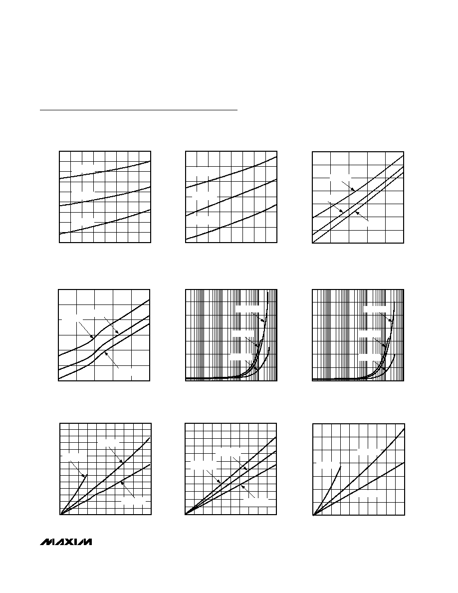
Typical Operating Characteristics
(V
CC
= +5V, V
EE
= 0V, C
L
= 15pF, V
OVERDRIVE
= 100mV, T
A
= +25°C, unless otherwise noted.)