 | –≠–ª–µ–∫—Ç—Ä–æ–Ω–Ω—ã–π –∫–æ–º–ø–æ–Ω–µ–Ω—Ç: MAX9130 | –°–∫–∞—á–∞—Ç—å:  PDF PDF  ZIP ZIP |
General Description
The MAX9130 is a single low-voltage differential signal-
ing (LVDS) line receiver ideal for applications requiring
high data rates, low power, and low noise. The device
is guaranteed to receive data at speeds up to 500Mbps
(250MHz).
The MAX9130 accepts an LVDS differential input and
translates it to an LVTTL/LVCMOS output. The fail-safe
feature sets the output high when the inputs are undriv-
en and open, terminated, or shorted. The device sup-
ports a wide common-mode input range, allowing a
ground potential difference and common-mode noise
between the driver and the receiver. The MAX9130
conforms to the ANSI/TIA/EIA-644 LVDS standard.
The MAX9130 operates from a single +3.3V supply,
and is specified for operation from -40∞C to +85∞C. It is
available in a space-saving 6-pin SC70 package. Refer
to the MAX9110/MAX9112 data sheet for single/dual
LVDS line drivers. Refer to the MAX9115 for a lower
speed (200Mbps) single LVDS line receiver in SC70.
Applications
Clock Distribution
Cellular Phone Base Stations
Digital Cross-Connects
Network Switches/Routers
DSLAMs
Features
o Space-Saving SC70 Package (50% Smaller than
SOT23)
o Guaranteed 500Mbps Data Rate
o Low 250ps (max) Pulse Skew
o High-Impedance LVDS Inputs When Powered Off
Allow Hot Swapping
o Conforms to ANSI TIA/EIA-644 LVDS Standard
o Single +3.3V Supply
o Fail-Safe Circuit Sets Output High for Undriven
Inputs (Open, Terminated, or Shorted)
o Low 150µA (typ) Supply Current in Fail-Safe Mode
MAX9130
Single 500Mbps LVDS Line Receiver in SC70
________________________________________________________________ Maxim Integrated Products
1
Ordering Information
19-2155; Rev 0; 10/01
For pricing, delivery, and ordering information, please contact Maxim/Dallas Direct! at
1-888-629-4642, or visit Maxim's website at www.maxim-ic.com.
PART
TEMP.
RANGE
PIN-
PACKAGE
TOP
MARK
MAX9130EXT-T
-40∞C to +85∞C
6 SC70-6
ABB
MAX9130
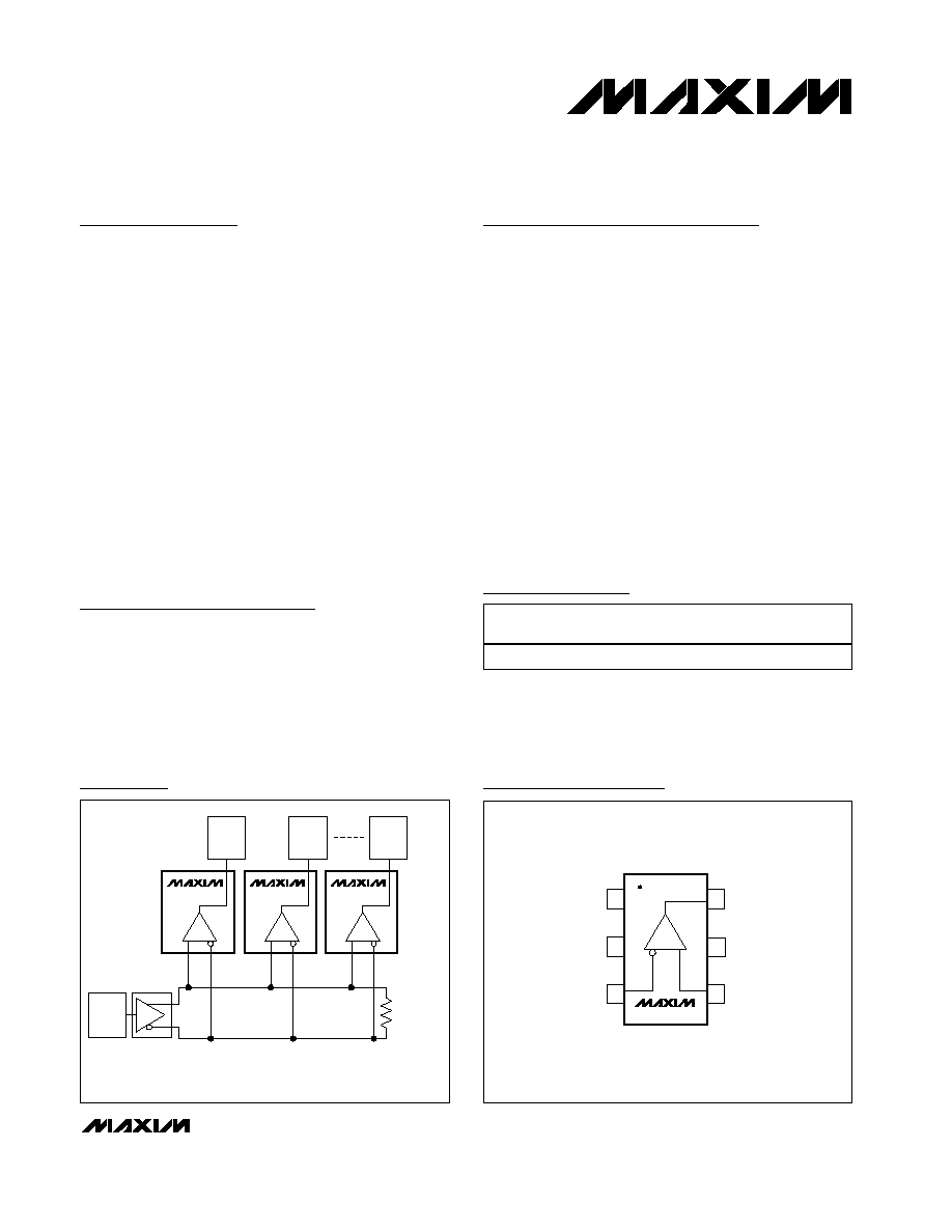
Rx
Tx
CLOCK
INPUT
CLOCK
SOURCE
CLOCK
INPUT
CLOCK
INPUT
MAX9130
Rx
LVDS SIGNALS
REFERENCE CLOCK DISTRIBUTION
USING MAX9130 IN A MULTIDROP CONFIGURATION
MAX9130
Rx
100
TERMINATION
Typical Application Circuit
GND
IN+
IN-
1
6
5
OUT
V
CC
MAX9130
SC70
TOP VIEW
2
3
4
GND
Pin Configuration

MAX9130
Single 500Mbps LVDS Line Receiver in SC70
2
_______________________________________________________________________________________
ABSOLUTE MAXIMUM RATINGS
DC ELECTRICAL CHARACTERISTICS
(V
CC
= +3.0V to +3.6V, differential input voltage |V
ID
| = 0.05V to 1.0V, input common voltage V
CM
= |V
ID
/2| to 2.4V - |V
ID
/2|,
T
A
= -40∞C to +85∞C, unless otherwise noted. Typical values at V
CC
= +3.3V, T
A
= +25∞C.) (Notes 2, 3)
Stresses beyond those listed under "Absolute Maximum Ratings" may cause permanent damage to the device. These are stress ratings only, and functional
operation of the device at these or any other conditions beyond those indicated in the operational sections of the specifications is not implied. Exposure to
absolute maximum rating conditions for extended periods may affect device reliability.
Note 1: Package leads soldered to a PC board having copper ground and V
CC
planes. Do not exceed Maximum Junction Temperature.
V
CC
to GND ...........................................................-0.3V to +4.0V
IN+, IN- to GND.....................................................-0.3V to +4.0V
OUT to GND ...............................................-0.3V to (V
CC
+ 0.3V)
Continuous Power Dissipation (T
A
= +70∞C)
6-Pin SC70 (derate 3.1mW/∞C above +70∞C) .............245 mW
Output Short to GND (OUT) (Note 1)........................................1s
Storage Temperature Range .............................-65∞C to +150∞C
Maximum Junction Temperature .....................................+150∞C
Operating Temperature Range ...........................-40∞C to +85∞C
ESD Protection
Human Body Model (IN+, IN-) .........................................±6kV
Lead Temperature (soldering, 10s) .................................+300∞C
PARAMETER
SYMBOL
CONDITIONS
MIN
TYP
MAX
UNITS
LVDS INPUTS (IN+, IN-)
Differential Input High Threshold
V
TH
50
mV
Differential Input Low Threshold
V
TL
-50
mV
0.05V
V
ID
0.6V
-20
20
Input Current
I
IN+
,
I
IN-
0.6V
<V
ID
1.0V
-25
25
µA
0.05V
V
ID
0.6V, V
CC
= 0
-20
20
Power-Off Input Current
I
INO
0.6V
<V
ID
1.0V, V
CC
= 0
-25
25
µA
R
IN1
V
CC
= +3.6V or 0, Figure 1
35
Input Resistance
R
IN2
V
CC
= +3.6V or 0, Figure 1
132
k
LVTTL/LVCMOS OUTPUT (OUT)
Inp uts op en or und r i ven shor t
or und r i ven 100
ter m i nati on
V
CC
- 0.3
Output High Voltage
V
OH
I
OH
= - 8.0m A
V
ID
= +50mV
V
CC
- 0.3
V
Output Low Voltage
V
OL
I
OL
= +8.0mA, V
ID
= -50mV
0.25
V
Output Short-Circuit Current
I
OS
V
ID
= +50mV, V
OUT
= 0
-125
mA
SUPPLY CURRENT
No load, inputs undriven (fail-safe)
150
300
µA
Supply Current
I
CC
No load, inputs driven
7
mA

MAX9130
Single 500Mbps LVDS Line Receiver in SC70
_______________________________________________________________________________________
3
AC ELECTRICAL CHARACTERISTICS
(V
CC
= +3.0V to +3.6V, C
L
= 15pF, differential input voltage |V
ID
| = 0.15V to 1.0V, input common voltage V
CM
= |V
ID
/2| to 2.4V - |V
ID
/2|, input rise and fall time = 1ns (20% to 80%), input frequency = 250MHz, T
A
= -40∞C to +85∞C, unless otherwise noted. Typical val-
ues at V
CC
= +3.3V, |V
ID
| = 0.2V, V
CM
= 1.2V, T
A
= +25∞C.) (Figures 2 and 3) (Notes 4 and 5)
PARAMETER
SYMBOL
CONDITIONS
MIN
TYP
MAX
UNITS
Differential Propagation Delay
High to Low
t
PHLD
1.2
1.8
3
ns
Differential Propagation Delay
Low to High
t
PLHD
1.2
1.8
3
ns
Differential Pulse Skew
|t
PHLD
-
t
PLHD
| (Note 6)
t
SKD1
250
ps
Differential Part-to-Part Skew
(Note 7)
t
SKD2
1.3
ns
Differential Part-to-Part Skew
(Note 8)
t
SKD3
1.8
ns
Rise Time
t
TLH
0.5
0.8
ns
Fall Time
t
THL
0.5
0.8
ns
Maximum Operating Frequency
(Note 9)
f
MAX
250
MHz
Note 2: Maximum and minimum limits over temperature are guaranteed by design and characterization. Devices are production
tested at T
A
= +25∞C.
Note 3: Current into a pin is defined as positive. Current out of a pin is defined as negative. All voltages are referenced to ground
except V
TH
, V
TL
, and V
ID
.
Note 4: AC parameters are guaranteed by design and characterization.
Note 5: C
L
includes scope probe and test jig capacitance.
Note 6: t
SKD1
is the magnitude difference of differential propagation delays. t
SKD1
= |t
PHLD
- t
PLHD
|.
Note 7: t
SKD2
is the magnitude difference of any differential propagation delays between parts operating over rated conditions at
the same V
CC
and within 5∞C of each other.
Note 8: t
SKD3
is the magnitude difference of any differential propagation delays between parts operating over rated conditions.
Note 9: f
MAX
pulse generator output conditions: rise time = fall time = 1ns (0% to 100%), 50% duty cycle, V
OH
= +1.3V, V
OL
= +1.1V.
MAX9130 output criteria: 60% to 40% duty cycle, V
OL
= 0.25V max, V
OH
= 2.7V min, load = 15pF.
MAX9130
Single 500Mbps LVDS Line Receiver in SC70
4
_______________________________________________________________________________________
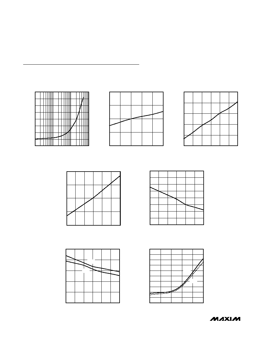
Typical Operating Characteristics
(V
CC
= +3.3V, C
L
= 15pF, |V
ID
| = 0.2V, V
CM
= 1.2V, input rise and fall time = 1ns (20% to 80%), input frequency = 250MHz, 50%
duty cycle, T
A
= +25∞C, unless otherwise noted.)
0
10
30
40
1
10
100
1000
SUPPLY CURRENT
vs. FREQUENCY
MAX9130 toc01
FREQUENCY (MHz)
SUPPLY CURRENT (mA)
20
6.00
5.50
5.00
4.50
4.00
-40
10
-15
35
60
85
SUPPLY CURRENT vs. TEMPERATURE
MAX9130 toc02
TEMPERATURE (
∞C)
SUPPLY CURRENT (mA)
-60
-65
-75
-70
-80
-85
3.0
3.3
3.6
OUTPUT SHORT-CIRCUIT CURRENT
vs. SUPPLY VOLTAGE
MAX9130 toc03
SUPPLY VOLTAGE (V)
OUTPUT SHORT-CIRCUIT CURRENT (mA)
3.60
3.40
3.20
3.00
2.80
3.0
3.3
3.6
OUTPUT HIGH VOLTAGE
vs. SUPPLY VOLTAGE
MAX9130 toc04
SUPPLY VOLTAGE (V)
OUTPUT HIGH VOLTAGE (V)
84.0
84.5
85.0
85.5
86.0
86.5
87.0
87.5
88.0
3.0
3.3
3.6
OUTPUT LOW VOLTAGE
vs. SUPPLY VOLTAGE
MAX9130 toc05
SUPPLY VOLTAGE (V)
OUTPUT LOW VOLTAGE (mV)
1.50
1.60
1.80
1.70
1.90
2.00
3.0
3.3
3.6
DIFFERENTIAL PROPAGATION DELAY
vs. SUPPLY VOLTAGE
MAX9130 toc06
SUPPLY VOLTAGE (V)
DIFFERENTIAL PROPAGATION DELAY (ns)
t
PHLD
t
PLHD
1.50
1.75
2.00
2.25
2.50
2.75
-40
10
-15
35
60
85
DIFFERENTIAL PROPAGATION DELAY
vs. TEMPERATURE
MAX9130 toc07
TEMPERATURE (
∞C)
DIFFERENTIAL PROPAGATION DELAY (ns)
t
PHLD
t
PLHD

MAX9130
Single 500Mbps LVDS Line Receiver in SC70
_______________________________________________________________________________________
5
10
20
40
30
50
60
3.0
3.3
3.6
DIFFERENTIAL PULSE SKEW
vs. SUPPLY VOLTAGE
MAX9130 toc08
SUPPLY VOLTAGE (V)
DIFFERENTIAL PULSE SKEW (ps)
0
20
60
40
80
100
-40
10
-15
35
60
85
DIFFERENTIAL PULSE SKEW
vs. TEMPERATURE
MAX9130 toc09
TEMPERATURE (
∞C)
DIFFERENTIAL PULSE SKEW (ps)
1.5
1.6
1.7
1.8
1.9
2.0
2.1
2.2
2.3
0.1
1.2
2.3
DIFFERENTIAL PROPAGATION DELAY
vs. COMMON-MODE VOLTAGE
MAX9130 toc10
COMMON-MODE VOLTAGE (V)
DIFFERENTIAL PROPAGATION DELAY (ns)
t
PHLD
t
PLHD
2.0
1.9
1.8
1.7
1.6
0.1
0.3
0.2
0.4
0.5
0.6
DIFFERENTIAL PROPAGATION DELAY
vs. DIFFERENTIAL INPUT VOLTAGE
MAX9130 toc11
DIFFERENTIAL INPUT VOLTAGE (V)
DIFFERENTIAL PROPAGATION DELAY (ns)
t
PHLD
t
PLHD
0.300
1.200
0.900
0.600
1.500
1.800
2.100
5
25
15
35
45
55
TRANSITION TIME
vs. LOAD CAPACITANCE
MAX9130 toc12
LOAD CAPACITANCE (pF)
TRANSITION TIME (ns)
t
TLH
t
THL
580
540
500
460
420
3.0
3.3
3.6
TRANSITION TIME vs. SUPPLY VOLTAGE
MAX9130 toc13
SUPPLY VOLTAGE (V)
TRANSITION TIME (ps)
t
THL
t
TLH
Typical Operating Characteristics (continued)
(V
CC
= +3.3V, C
L
= 15pF, |V
ID
| = 0.2V, V
CM
= 1.2V, input rise and fall time = 1ns (20% to 80%), input frequency = 250MHz, 50%
duty cycle, T
A
= +25∞C, unless otherwise noted.)