 | –≠–ª–µ–∫—Ç—Ä–æ–Ω–Ω—ã–π –∫–æ–º–ø–æ–Ω–µ–Ω—Ç: MAX9171 | –°–∫–∞—á–∞—Ç—å:  PDF PDF  ZIP ZIP |

General Description
The MAX9171/MAX9172 single/dual low-voltage differential
signaling (LVDS) receivers are designed for high-speed
applications requiring minimum power consumption,
space, and noise. Both devices support switching rates
exceeding 500Mbps while operating from a single 3.3V
supply.
The MAX9171 is a single LVDS receiver and the
MAX9172 is a dual LVDS receiver. Both devices con-
form to the ANSI TIA/EIA-644 LVDS standard and con-
vert LVDS to LVTTL/LVCMOS-compatible outputs. A
fail-safe feature sets the outputs high when the inputs
are undriven and open, terminated, or shorted. The
MAX9171/MAX9172 are available in 8-pin SO packages
and space-saving thin QFN and SOT23 packages.
For lower skew devices, refer to the MAX9111/ MAX9113
data sheet.
Applications
Multipoint Backplane Interconnect
Laser Printers
Digital Copiers
Cellular Phone Base Stations
LCD Displays
Network Switches/Routers
Clock Distribution
Features
o Input Accepts LVDS and LVPECL
o In-Path Fail-Safe Circuit
o Space-Saving 8-Pin QFN and SOT23 Packages
o Fail-Safe Circuitry Sets Output High for Open,
Undriven Shorted, or Undriven Terminated Output
o Flow-Through Pinout Simplifies PC Board Layout
o Guaranteed 500Mbps Data Rate
o Second Source to DS90LV018A and DS90LV028A
(SO Packages Only)
o Conforms to ANSI TIA/EIA-644 Standard
o 3.3V Supply Voltage
o -40∞C to +85∞C Operating Temperature Range
o Low Power Dissipation
MAX9171/MAX9172
Single/Dual LVDS Line Receivers with
"In-Path" Fail-Safe
________________________________________________________________ Maxim Integrated Products
1
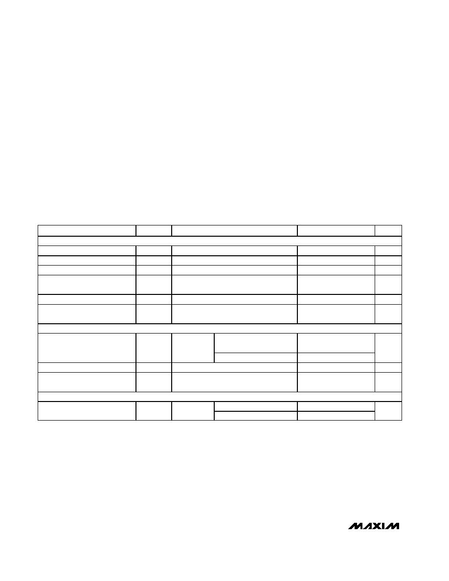
Ordering Information
19-2578; Rev 0; 10/02
For pricing, delivery, and ordering information, please contact Maxim/Dallas Direct! at
1-888-629-4642, or visit Maxim's website at www.maxim-ic.com.
PART
TEMP RANGE
PIN-
PACKAGE
TOP
MARK
MAX9171EKA-T
-40
∞C to +85∞C
8 SOT23-8
AALX
MAX9171ESA
-40
∞C to +85∞C
8 SO
--
MAX9171ETA*
-40
∞C to +85∞C
8 Thin QFN
--
MAX9172EKA-T
-40
∞C to +85∞C
8 SOT23-8
AALY
MAX9172ESA
-40
∞C to +85∞C
8 SO
--
MAX9172ETA*
-40
∞C to +85∞C
8 Thin QFN
--
1
2
3
4
5
6
7
8
SO/QFN*
IN-
IN+
N.C.
N.C.
GND
N.C.
OUT
V
CC
IN-
IN+
N.C.
N.C.
GND
N.C.
OUT
V
CC
IN1-
IN1+
IN2+
IN2-
GND
OUT2
OUT1
V
CC
IN1-
IN1+
IN2-
OUT2
GND
IN2+
OUT1
V
CC
MAX9171
1
2
3
4
5
6
7
8
SO/QFN*
MAX9172
1
2
3
4
5
6
7
8
SOT23
MAX9172
1
2
3
4
8
7
6
5
SOT23
MAX9171
Pin Configurations
*Future product--contact factory for availability.
MAX9171/MAX9172
Single/Dual LVDS Line Receivers with
"In-Path" Fail-Safe
2
_______________________________________________________________________________________
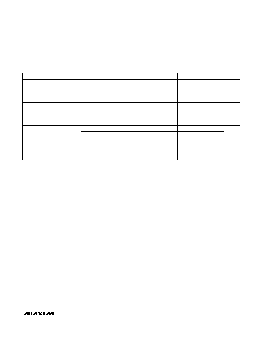
ABSOLUTE MAXIMUM RATINGS
ELECTRICAL CHARACTERISTICS
(V
CC
= 3.0V to 3.6V, differential input voltage |V
ID
| = 0.1V to 1.2V, receiver input voltage = 0 to V
CC
, common-mode voltage V
CM
=
|V
ID
/2| to (V
CC
- |V
ID
/2|), T
A
= -40∞C to +85∞C, unless otherwise noted. Typical values are at V
CC
= 3.3V, |V
ID
| = 0.2V, V
CM
= 1.2V,
T
A
= +25∞C.) (Notes 1, 2)
Stresses beyond those listed under "Absolute Maximum Ratings" may cause permanent damage to the device. These are stress ratings only, and functional
operation of the device at these or any other conditions beyond those indicated in the operational sections of the specifications is not implied. Exposure to
absolute maximum rating conditions for extended periods may affect device reliability.
V
CC
to GND ...........................................................-0.3V to +4.0V
IN_+, IN_- to GND .................................................-0.3V to +4.0V
OUT_ to GND ............................................-0.3V to (V
CC
+ 0.3V)
Continuous Power Dissipation (T
A
= +70∞C)
8-Pin SOT23 (derate 8.9mW/∞C above +70∞C) ...........714mW
8-Pin SO (derate 5.9mW/∞C above +70∞C) .................471mW
8-Pin QFN (derate 24.4mW/∞C above +70∞C) ..........1951mW
Operating Temperature Range ..........................-40∞C to +85∞C
Junction Temperature .....................................................+150∞C
Storage Temperature Range ............................-65∞C to +150∞C
ESD Protection
Human Body Model (IN_+, IN_-) ...................................±13kV
Lead Temperature (soldering, 10s) ................................+300∞C
PARAMETER
SYMBOL
CONDITIONS
MIN
TYP
MAX
UNITS
LVDS INPUTS (IN_+, IN_-)
Differential Input High Threshold
V
TH
Figure 1
-40
0
mV
Differential Input Low Threshold
V
TL
Figure 1
-100
-40
mV
Input Current (Noninverting Input)
I
IN+
Figure 1
+0.5
-2.1
-5.0
µA
Power-Off Input Current
(Noninverting Input)
I
IN+OFF
V
IN+
= 0 to 3.6V, V
IN-
= 0 to 3.6V, V
CC
= 0
or open (Figure 1)
-0.5
0
+0.5
µA
Input Current (Inverting Input)
I
IN-
Figure 1
-0.5
+4.4
+10.0
µA
Power-Off Input Current
(Inverting Input)
I
IN-OFF
V
IN+
= 0 to 3.6V, V
IN-
= 0 to 3.6V, V
CC
= 0
or open (Figure 1)
-0.5
0
+0.5
µA
LVCMOS/LVTTL OUTPUTS (OUT_)
Open, undriven short, or
undriven parallel termination
2.7
3.2
Output High Voltage
V
OH
I
OH
= -4.0mA
V
ID
= 0V
2.7
3.2
V
Output Low Voltage
V
OL
I
OL
= 4.0mA, V
ID
= -100mV
0.1
0.4
V
Output Short-Circuit Current
I
OS
V
OUT_
= 0 (Note 3)
-45
-77
-120
mA
POWER SUPPLY
MAX9171
3.6
6
Supply Current
I
CC
Inputs open
MAX9172
7.0
9
mA
MAX9171/MAX9172
Single/Dual LVDS Line Receivers with
"In-Path" Fail-Safe
_______________________________________________________________________________________
3
Note 1: Current into a pin is defined as positive. Current out of a pin is defined as negative. All voltages are referenced to GND
except V
TH
, V
TL
, and V
ID
.
Note 2: All devices are 100% production tested at T
A
= +25∞C and are guaranteed by design for T
A
= -40∞C to +85∞C, as specified.
Note 3: Short only one output at a time. Do not exceed the absolute maximum junction temperature specification.
Note 4: AC parameters are guaranteed by design and not production tested.
Note 5: C
L
includes scope probe and test jig capacitance.
Note 6: Pulse generator output conditions: t
R
= t
F
< 1ns (0% to 100%), frequency = 250MHz, 50% duty cycle, V
OH
= 1.3V, V
OL
= 1.1V.
Note 7: t
SKD1
is the magnitude of the difference of differential propagation delays in a channel. t
SKD1
= |t
PHLD
- t
PLHD
|.
Note 8: t
SKD2
is the magnitude of the difference of the t
PLHD
or t
PHLD
of one channel and the t
PLHD
or t
PHLD
of the other channel
on the same part.
Note 9: t
SKD3
is the magnitude of the difference of any differential propagation delays between parts at the same V
CC
and within
5∞C of each other.
Note 10: t
SKD4
is the magnitude of the difference of any differential propagation delays between parts operating over the rated
supply and temperature ranges.
SWITCHING CHARACTERISTICS
(V
CC
= 3.0V to 3.6V, C
L
= 15pF, |V
ID
| = 0.2V, V
CM
= 1.2V, T
A
= -40∞C to +85∞C, unless otherwise noted. Typical values are at V
CC
=
3.3V, T
A
= +25∞C.) (Notes 4, 5, 6)
PARAMETER
SYMBOL
CONDITIONS
MIN
TYP
MAX
UNITS
Differential Propagation Delay
High to Low
t
PHLD
Figures 2, 3
1.0
1.65
2.5
ns
Differential Propagation Delay
Low to High
t
PLHD
Figures 2, 3
1.0
1.62
2.5
ns
Differential Pulse Skew
|t
PHLD
- t
PLHD
|
t
SKD1
Figures 2, 3 (Note 7)
30
400
ps
Differential Channel-to-Channel
Skew (MAX9172)
t
SKD2
Figures 2, 3 (Note 8)
40
500
ps
t
SKD3
Figures 2, 3 (Note 9)
1
Differential Part-to-Part Skew
t
SKD4
Figures 2, 3 (Note 10)
1.5
ns
Rise Time
t
TLH
Figures 2, 3
0.55
0.8
ns
Fall Time
t
THL
Figures 2, 3
0.51
0.8
ps
Maximum Operating Frequency
f
MAX
All channels switching, V
OL(MAX)
= 0.4V,
V
OH(MIN)
= 2.7V, 40% < duty cycle < 60%
250
300
MHz
MAX9171/MAX9172
Single/Dual LVDS Line Receivers with
"In-Path" Fail-Safe
4
_______________________________________________________________________________________
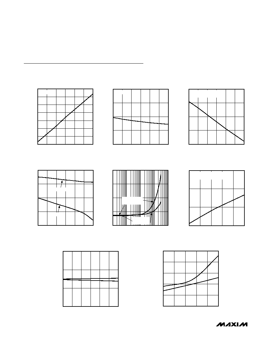
Typical Operating Characteristics
(V
CC
= 3.3V, V
CM
= 1.2V, |V
ID
| = 0.2V, f
IN
= 200MHz, C
L
= 15pF, T
A
= +25∞C, unless otherwise specified.)
OUTPUT HIGH VOLTAGE
vs. SUPPLY VOLTAGE
MAX9171 toc01
SUPPLY VOLTAGE (V)
OUTPUT HIGH VOLTAGE (V)
3.5
3.4
3.3
3.2
3.1
3.0
3.1
3.2
3.3
3.4
3.5
3.6
2.9
3.0
3.6
I
OH
= -4mA
OUTPUT LOW VOLTAGE
vs. SUPPLY VOLTAGE
MAX9171 toc02
SUPPLY VOLTAGE (V)
OUTPUT LOW VOLTAGE (mV)
3.5
3.4
3.3
3.2
3.1
85
90
95
100
80
3.0
3.6
I
OL
= +4mA
OUTPUT SHORT-CIRCUIT CURRENT
vs. SUPPLY VOLTAGE
MAX9171 toc03
SUPPLY VOLTAGE (V)
OUTPUT SHORT-CIRCUIT CURRENT (mA)
3.5
3.4
3.3
3.2
3.1
-80
-75
-70
-65
-85
3.0
3.6
V
ID
= +200mV, OUTPUT
SHORTED TO GROUND
DIFFERENTIAL THRESHOLD VOLTAGE
vs. SUPPLY VOLTAGE
MAX9171 toc04
SUPPLY VOLTAGE (V)
DIFFERENTIAL THRESHOLD VOLTAGE (mV)
3.5
3.4
3.3
3.2
3.1
-50
-45
-40
-35
-55
3.0
3.6
HIGH-LOW
LOW-HIGH
MAX9172 SUPPLY CURRENT
vs. FREQUENCY
MAX9171 toc05
FREQUENCY (MHz)
SUPPLY CURRENT (mA)
100
10
1
10
20
30
40
0
0.1
1000
BOTH CHANNELS
SWITCHING
ONE CHANNEL
SWITCHING
MAX9172 SUPPLY CURRENT
vs. TEMPERATURE
MAX9171 toc06
TEMPERATURE (
∞C)
SUPPLY CURRENT (mA)
60
35
10
-15
7
8
9
6
-40
85
f = 1MHz
BOTH CHANNELS SWITCHING
DIFFERENTIAL PROPAGATION DELAY
vs. SUPPLY VOLTAGE
MAX9171 toc07
SUPPLY VOLTAGE (V)
DIFFERENTIAL PROPAGATION DELAY (ns)
3.5
3.4
3.3
3.2
3.1
1.5
2.0
2.5
1.0
3.0
3.6
t
PHLD
t
PLHD
DIFFERENTIAL PROPAGATION DELAY
vs. TEMPERATURE
MAX9171 toc08
TEMPERATURE (
∞C)
DIFFERENTIAL PROPAGATION DELAY (ns)
60
35
10
-15
1.6
1.7
1.8
1.9
2.0
1.5
-40
85
t
PHLD
t
PLHD
MAX9171/MAX9172
Single/Dual LVDS Line Receivers with
"In-Path" Fail-Safe
_______________________________________________________________________________________
5
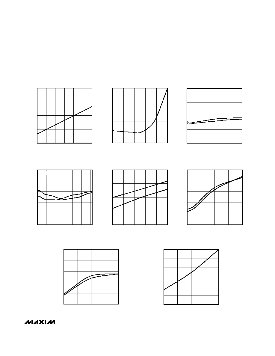
DIFFERENTIAL PULSE SKEW
vs. SUPPLY VOLTAGE
MAX9171 toc09
SUPPLY VOLTAGE (V)
DIFFERENTIAL PULSE SKEW (ps)
3.5
3.4
3.3
3.2
3.1
30
60
90
120
0
3.0
3.6
DIFFERENTIAL PULSE SKEW
vs. TEMPERATURE
MAX9171 toc10
TEMPERATURE (
∞C)
DIFFERENTIAL PULSE SKEW (ps)
60
35
10
-15
40
80
120
160
200
0
-40
85
DIFFERENTIAL PROPAGATION DELAY
vs. DIFFERENTIAL INPUT VOLTAGE
MAX9171 toc11
DIFFERENTIAL INPUT VOLTAGE (mV)
DIFFERENTIAL PROPAGATION DELAY (ns)
2100
1600
1100
600
1.5
2.0
2.5
3.0
1.0
100
2600
f
IN
= 20MHz
t
PHLD
t
PLHD
DIFFERENTIAL PROPAGATION DELAY
vs. COMMON-MODE VOLTAGE
MAX9171 toc12
COMMON-MODE VOLTAGE (V)
DIFFERENTIAL PROPAGATION DELAY (ns)
2.6
2.1
1.6
1.1
0.6
1.3
1.6
1.9
2.2
2.5
1.0
0.1
3.1
f
IN
= 20MHz
t
PHLD
t
PLHD
TRANSITION TIME vs. TEMPERATURE
MAX9171 toc13
TEMPERATURE (
∞C)
TRANSITION TIME (ps)
60
35
10
-15
400
500
600
700
300
-40
85
t
TLH
t
THL
DIFFERENTIAL PROPAGATION DELAY
vs. LOAD
MAX9171 toc14
LOAD (pF)
DIFFERENTIAL PROPAGATION DELAY (ns)
40
30
20
1.6
1.8
2.0
2.2
2.4
1.4
10
50
f
IN
= 20MHz
t
PHLD
t
PLHD
TRANSITION TIME vs. LOAD
MAX9171 toc15
LOAD (pF)
TRANSITION TIME (ps)
40
30
20
500
900
1300
1700
2100
100
10
50
t
TLH
t
THL
DIFFERENTIAL PULSE SKEW
vs. INPUT TRANSITION TIME
MAX9171 toc16
INPUT TRANSITION TIME (ns)
DIFFERENTIAL PULSE SKEW (ps)
2.5
2.0
1.5
50
100
150
200
250
300
0
1.0
3.0
Typical Operating Characteristics (continued)
(V
CC
= 3.3V, V
CM
= 1.2V, |V
ID
| = 0.2V, f
IN
= 200MHz, C
L
= 15pF, T
A
= +25∞C, unless otherwise specified.)