 | –≠–ª–µ–∫—Ç—Ä–æ–Ω–Ω—ã–π –∫–æ–º–ø–æ–Ω–µ–Ω—Ç: MAX9202 | –°–∫–∞—á–∞—Ç—å:  PDF PDF  ZIP ZIP |
General Description
The MAX9201/MAX9202/MAX9203 high-speed, low-
power, quad/dual/single comparators feature TTL logic
outputs with active internal pullups. Fast propagation
delay (7ns typ at 5mV overdrive) makes these devices
ideal for fast A/D converters and sampling circuits, line
receivers, V/F converters, and many other data-discrim-
ination, signal restoration applications.
All comparators can be powered from separate analog
and digital power supplies or from a single combined
supply voltage. The analog input common-mode range
includes the negative rail, allowing ground sensing
when powered from a single supply. The MAX9201/
MAX9202/MAX9203 consume only 9mW per compara-
tor when powered from a +5V supply.
The MAX9202/MAX9203 feature output latches with TTL
compatible inputs. The comparator output states are
held when the latch inputs are driven low. The
MAX9201 provides all the same features as the
MAX9202/MAX9203 with the exception of the latches.
The MAX9201/MAX9202/MAX9203 are lower power and
lower cost upgrades to the MAX901/MAX902/MAX903
offering a 50% power savings and smaller packaging.
________________________Applications
____________________________Features
o Fast 7ns Propagation Delay
o Low 9mW/Comparator Power Consumption
o Separate Analog and Digital Supplies
o Flexible Analog Supply: +5V to +10V or ±5V
o Input Voltage Range Includes
Negative Supply Rail
o TTL-Compatible Outputs
o TTL-Compatible Latch Inputs
(MAX9202/MAX9203)
o Available in Space-Saving Packages
8-Pin SOT23 (MAX9203)
14-Pin TSSOP (MAX9202)
16-Pin TSSOP (MAX9201)
MAX9201/MAX9202/MAX9203
Low-Cost, 7ns, Low-Power
Voltage Comparators
________________________________________________________________ Maxim Integrated Products
1
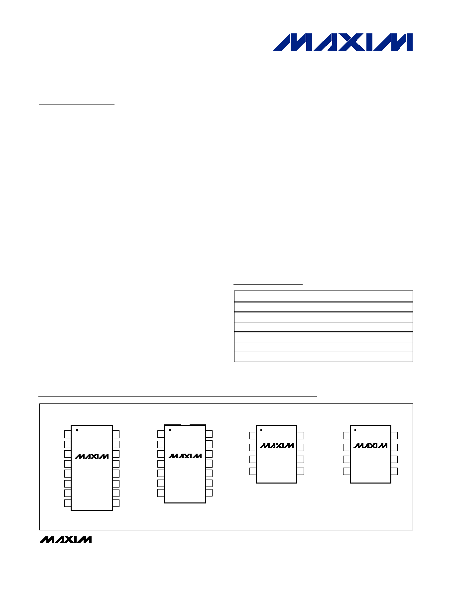
TOP VIEW
14
13
12
11
10
9
8
1
2
3
4
5
6
7
V
CC
N.C.
OUTB
LATCHB
LATCHA
GND
INA+
INA-
MAX9202
V
DD
INB+
INB-
V
EE
N.C.
OUTA
SO/TSSOP
16
15
14
13
12
11
10
9
1
2
3
4
5
6
7
8
INA-
IND-
IND+
V
CC
OUTD
OUTC
V
DD
INC+
INC-
MAX9201
SO/TSSOP
INA+
GND
V
EE
OUTA
OUTB
INB+
INB-
IN-
V
EE
LATCH
1
2
8
7
V
CC
IN+
OUT
GND
V
DD
SOT23
3
4
6
5
MAX9203
GND
LATCH
V
EE
1
2
8
7
V
DD
OUT
IN+
IN-
V
CC
SO
3
4
6
5
MAX9203
Pin Configurations
For price, delivery, and to place orders, please contact Maxim Distribution at 1-888-629-4642,
or visit Maxim's website at www.maxim-ic.com.
PART
TEMP RANGE
PIN-PACKAGE
MAX9201EUE
-40∞C to +85∞C
16 TSSOP
MAX9201ESE
-40∞C to +85∞C
16 Narrow SO
MAX9202EUD
-40∞C to +85∞C
14 TSSOP
MAX9202ESD
-40∞C to +85∞C
14 Narrow SO
MAX9203EKA-T
-40∞C to +85∞C
8 SOT23-8
MAX9203ESA
-40∞C to +85∞C
8 Narrow SO
Ordering Information
High-Speed A/D
Converters
High-Speed V/F
Converters
Line Receivers
High-Speed Signal
Squaring/Restoration
Threshold Detectors
Input Trigger Circuitry
High-Speed Data
Sampling
PWM Circuits
19-1936; Rev 1; 1/05

MAX9201/MAX9202/MAX9203
Low Cost, 7ns, Low-Power
Voltage Comparators
2
_______________________________________________________________________________________
ABSOLUTE MAXIMUM RATINGS
ELECTRICAL CHARACTERISTICS
(V
CC
= +5V, V
EE
= -5V, V
DD
= +5V, GND = 0, V
CM
= 0, LATCH_ = logic high, T
A
= -40
∞C to +85∞C. Typical values are at T
A
= +25
∞C,
unless otherwise noted.) (Note 1)
Stresses beyond those listed under "Absolute Maximum Ratings" may cause permanent damage to the device. These are stress ratings only, and function-
al operation of the device at these or any other conditions beyond those indicated in the operational sections of the specifications is not implied. Exposure
to absolute maximum rating conditions for extended periods may affect device reliability.
Analog Supply Voltage (V
CC
- V
EE
) .....................................+12V
Digital Supply Voltage (V
DD
) .................................................+7V
Differential Input Voltage..................(V
EE
- 0.3V) to (V
CC
+ 0.3V)
Common Mode Input Voltage ..........(V
EE
- 0.3V) to (V
CC
+ 0.3V)
Latch Input Voltage
(MAX9202/MAX9203 only) .....................-0.3V to (V
DD
+ 0.3V)
Output Short-Circuit Duration
To GND ......................................................................Continuous
To V
DD
..................................................................................1min
Continuous Power Dissipation (T
A
= +70∞C)
8-Pin SOT23-8 (derate 9.1mW/∞C above +70∞C) ...727mW/∞C
8-Pin SO (derate 5.9mW/∞C above +70∞C).............471mW/∞C
14-Pin TSSOP (derate 9.1mW/∞C above +70∞C) ....727mW/∞C
14-Pin SO (derate 8.3mW/∞C above +70∞C)...........667mW/∞C
16-Pin TSSOP (derate 9.4mW/∞C above +70∞C) ....755mW/∞C
16-Pin SO (derate 8.7mW/∞C above +70∞C)...........696mW/∞C
Operating Temperature Range ...........................-45∞C to +85∞C
Junction Temperature ......................................................+150∞C
Storage Temperature Range ............................-65∞C to +150∞C
Lead Temperature (soldering, 10s) ................................+300∞C
PARAMETER
SYMBOL
CONDITIONS
MIN
TYP
MAX
UNITS
Analog Supply Voltage Range
V
CC
- V
EE
Referenced to V
EE
4.75
10.5
V
Digital Supply Voltage Range
V
DD
Referenced to GND
4.75
5.25
V
T
A
= +25
∞C
1
4
Input Offset Voltage
V
OS
V
CM
= 0,
V
OUT
= 1.4V
T
A
= -40
∞C to +85∞C
7.5
mV
T
A
= +25
∞C
1.25
5
Input Bias Current
I
B
I
IN+
or I
IN-
T
A
= -40
∞C to +85∞C
7.0
µA
T
A
= +25
∞C
50
250
Input Offset Current
I
OS
V
CM
= 0,
V
OUT
= 1.4V
T
A
= -40
∞C to +85∞C
450
nA
Common-Mode Input Voltage
Range
V
CM
Note 2
V
EE
- 0.1
V
C C
-
2.25
V
T
A
= +25
∞C
50
150
Common-Mode Rejection
Ratio
CMRR
- 5.1V <
V
C M
< +2.75V
V
OU T
= 1.4V
T
A
= -40
∞C to +85∞C
250
µV/V
T
A
= +25
∞C
50
150
Power-Supply Rejection Ratio
PSRR
Note 3
T
A
= -40
∞C to +85∞C
250
µV/V
Output High Voltage
V
OH
(V
IN+
- V
IN-
) > 250mV, I
SOURCE
= 1mA
3.0
3.5
V
Output Low Voltage
V
OL
(V
IN+
- V
IN-
) < -250mV, I
SINK
= 8mA
0.25
0.4
V
Latch Input Threshold Voltage
High
V
LH
Note 4
1.4
2
V
Latch Input Threshold Voltage
Low
V
LL
Note 4
0.8
1.4
V
Latch Input Current High
I
LH
V
LH
= 3.0V, Note 4
0.5
3
µA
Latch Input Current Low
I
LL
V
LL
= 0.3V, Note 4
0.5
3
µA
Input Capacitance
C
IN
4
pF
Differential Input Impedance
R
IND
5
M
Common-Mode Input
Impedance
R
INCM
5.5
M
MAX9201
4.7
7
MAX9202
2.5
4.0
Positive Analog Supply
Current
I
CC
Note 5
MAX9203
1.3
2
mA

MAX9201/MAX9202/MAX9203
Low Cost, 7ns, Low-Power
Voltage Comparators
_______________________________________________________________________________________
3
Note 1: All devices are 100% production tested at T
A
= +25∞C. All temperature limits are guaranteed by design.
Note 2: Inferred by CMRR test.
Note 3: Tested for +4.75V < V
CC
< +5.25V, and -5.25V < V
EE
< -4.75V with V
DD
= +5V, although permissible analog power-supply
range is 4.75V < V
CC
< +10.5V for single supply operation with V
EE
grounded.
Note 4: Specification does not apply to MAX9201.
Note 5: I
CC
tested for 4.75V < V
CC
< +10.5V with V
EE
grounded. I
EE
tested for -5.25V < V
EE
< -4.75V with V
CC
= +5V. I
DD
tested for
+4.75V < V
DD
< +5.25V with all comparator outputs low, worst-case condition.
Note 6: Guaranteed by design. Times are for 100mV step inputs (see propagation delay characteristics in Figures 2 and 3)
Note 7: Maximum difference in propagation delay between two comparators in the MAX9201/MAX9202.
PARAMETER
SYMBOL
CONDITIONS
MIN
TYP
MAX
UNITS
MAX9201
3.4
5.0
MAX9202
1.8
3.0
Negative Analog Supply
Current
I
EE
Note 5
MAX9203
1.0
1.6
mA
MAX9201
2
3.0
MAX9202
1
1.5
Digital Supply Current
I
DD
Note 5
MAX9203
0.5
0.8
mA
MAX9201
33
44
MAX9202
17
24
Power Dissipation
P
D
V
CC
= V
DD
= +5V,
V
EE
= 0V
MAX9203
9
13
mW
TIMING CHARACTERISTICS
(V
CC
= +5V, V
EE
= -5V, V
DD
= +5V, GND = 0, V
CM
= 0, LATCH_ = logic high, T
A
= -40∞C to +85∞C. Typical values are at
T
A
= +25∞C, unless otherwise noted.) (Notes 1, 6)
ELECTRICAL CHARACTERISTICS (continued)
(V
CC
= +5V, V
EE
= -5V, V
DD
= +5V, GND = 0, V
CM
= 0, LATCH_ = logic high, T
A
= -40
∞C to +85∞C. Typical values are at T
A
= +25
∞C,
unless otherwise noted.) (Note 1)
PARAMETER
SYMBOL
CONDITIONS
MIN
TYP
MAX
UNITS
T
A
= +25
∞C
7
9
Input-to-Output High
Response Time
t
PD+
V
OD
= 5mV,
C
L
= 15pF,
I
OUT
= 2mA
T
A
= -40
∞C to +85∞C
12
ns
T
A
= +25
∞C
7
9
Input-to-Output Low
Response Time
t
PD-
V
OD
= 5mV,
C
L
= 15pF,
I
OUT
= 2mA
T
A
= -40
∞C to +85∞C
12
ns
Rise Time
t
R
C
L
= 15pF,
I
OUT
= 2mA
T
A
= +25
∞C
2.0
ns
Fall Time
t
F
C
L
= 15pF,
I
OUT
= 2mA
T
A
= +25
∞C
1.0
ns
T
A
= +25
∞C
0.5
1.5
Difference in Response Time
Between Outputs
t
PD
Note 7
T
A
= -40
∞C to +85∞C
2.5
ns
Latch Disable to Output High
Delay
t
PD
+(D)
Note 4
10
ns
Latch Disable to Output Low
Delay
t
PD
-(D)
Note 4
10
ns
Minimum Setup Time
t
S
Note 4
2
ns
Minimum Hold Time
t
N
Note 4
1
ns
Minimum Latch Disable
Pulse Width
t
PW
(D)
Note 4
8
ns

MAX9201/MAX9202/MAX9203
Low Cost, 7ns, Low-Power
Voltage Comparators
4
_______________________________________________________________________________________
-1.5
-0.5
-1.0
0.5
0
1.0
1.5
-40
10
-15
35
60
85
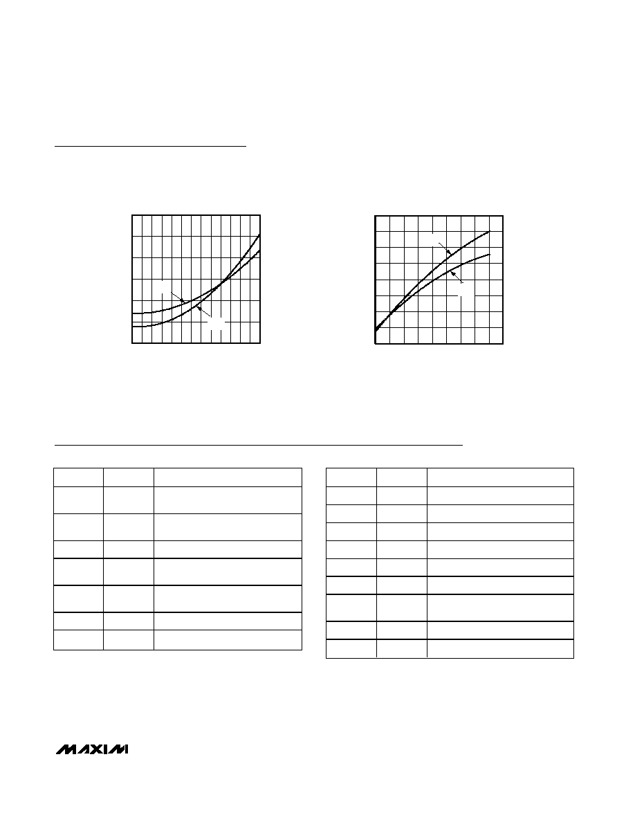
INPUT OFFSET VOLTAGE vs. TEMPERATURE
MAX9201 toc01
TEMPERATURE (
∞C)
INPUT OFFSET VOLTAGE (mV)
2.8
3.2
3.0
3.6
3.4
3.8
4.0
0
4
6
2
8
10
12
OUTPUT HIGH VOLTAGE (V
OH
)
vs. LOAD CURRENT
MAX9201 toc03
LOAD CURRENT (mA)
OUTPUT HIGH VOLTAGE (V)
T
A
= -40
∞C
T
A
= +85
∞C
T
A
= +25
∞C
0
50
100
150
200
250
300
350
400
0
4
2
6
8
10
12
OUTPUT LOW VOLTAGE (V
OL
)
vs. LOAD CURRENT
MAX9201 toc04
LOAD CURRENT (mA)
OUTPUT LOW VOLTAGE (mV)
T
A
= +85
∞C
T
A
= +25
∞C
T
A
= -40
∞C
5.0
6.0
5.5
7.0
6.5
8.0
7.5
8.5
9.5
9.0
10.0
0
10 15 20
5
25 30 35
45
40
50
RESPONSE TIME vs. INPUT OVERDRIVE
MAX9201 toc06
INPUT OVERDRIVE (mV)
RESPONSE TIME (ns)
t
PD-
t
PD+
0.8
0.9
1.0
1.1
1.2
1.3
1.4
1.5
1.6
5
6
7
8
9
10
I
CC
SUPPLY CURRENT (PER COMPARATOR)
vs. V
CC
SUPPLY VOLTAGE
MAX9201 toc05
VCC SUPPLY VOLTAGE (V)
I CC
SUPPLY CURRENT (mA)
TA = +85∞C
TA = +25∞C
TA = -40∞C
V
EE
= GND
Typical Operating Characteristics
(V
CC
= +5V, V
EE
= -5V, V
DD
= +5V, GND = 0, V
CM
= 0, LATCH_ = logic high, V
OUT
= 1.4V, T
A
= +25
∞C, unless otherwise noted.)
0.4
0.8
0.6
1.2
1.0
1.6
1.4
1.8
-40
10
-15
35
60
85
INPUT BIAS CURRENT vs. TEMPERATURE
MAX9201 toc02
TEMPERATURE (
∞C)
INPUT BIAS CURRENT (
µ
A)
VCM = 0
MAX9201/MAX9202/MAX9203
Low Cost, 7ns, Low-Power
Voltage Comparators
_______________________________________________________________________________________
5
Typical Operating Characteristics (continued)
(V
CC
= +5V, V
EE
= -5V, V
DD
= +5V, GND = 0, V
CM
= 0, LATCH_ = logic high, V
OUT
= 1.4V, T
A
= +25
∞C, unless otherwise noted.)
Pin Description
6.0
7.0
6.5
8.5
8.0
7.5
9.5
9.0
10.0
0
30
40
10
20
50
60
70
80
90
RESPONSE TIME vs. LOAD CAPACITANCE
(5mV OVERDRIVE, R
LOAD
= 2.4k
)
MAX9201 toc08
LOAD CAPACITANCE (pF)
RESPONSE TIME (ns)
t
PD-
t
PD+
6.5
7.0
6.8
7.5
7.3
7.8
8.0
-40 -30 -20 -10 0 10 20 30 40 50 60 70 80 90
RESPONSE TIME vs. TEMPERATURE
(5mV OVERDRIVE)
MAX9201 toc07
TEMPERATURE (
∞C)
RESPONSE TIME (ns)
t
PD-
t
PD+
PIN
NAME
FUNCTION
1, 8, 9,
16
IN_-
Negative Input (Channels A, B, C,
D)
2, 7, 10,
15
IN_+
Positive Input (Channels A, B, C,
D)
3
GND
Ground
4, 5, 12,
13
OUT_
Output (Channels A, B, C, D)
6
V
EE
Negative Analog Supply and
Substrate
11
V
DD
Positive Digital Supply
14
V
CC
Positive Analog Supply
PIN
NAME
FUNCTION
1, 8
IN_-
Negative Input (Channels A, B)
2, 9
IN_+
Positive Input (Channels A, B)
3
GND
Ground
4, 11
LATCH_
Latch Input (Channels A, B)
5, 12
OUT_
Output (Channels A, B)
6, 13
N.C.
No Connection
7
V
EE
Negative Analog Supply and
Substrate
10
V
DD
Positive Digital Supply
14
V
CC
Positive Analog Supply
MAX9201
MAX9202