General Description
The MAX9374 and MAX9374A are 2.0GHz differential
LVPECL-to-LVDS translators and are designed for tele-
com applications. They feature 250ps propagation
delay. The differential output conforms to the ANSI
TIA/EIA-644 LVDS standard. The inputs are biased with
internal resistors such that the output is differential low
when inputs are open. An on-chip V
BB
reference output
is available for single-ended operation.
The MAX9374 is designed for low-voltage operation
from a 2.375V to 2.625V power supply for use in 2.5V
systems. The MAX9374A is designed for 3.0V to 3.6V
operation in systems with a nominal 3.3V supply. Both
devices are offered in industry-standard 8-pin SOT23
and SO packages.
Applications
Precision Clock Buffer
Low-Jitter Data Repeater
Central Office Clock Distribution
DSLAM/DLC
Base Station
Mass Storage
Features
o Guaranteed 2.0GHz Operating Frequency
o 250ps (typ) Propagation Delay
o 1.0ps RMS Jitter (typ)
o 2.375V to 2.625V Low-Voltage Supply Range
(MAX9374)
o On-Chip V
BB
Reference for Single-Ended Input
o Output Low for Open Inputs
o Output Conforms to ANSI TIA/EIA-644 LVDS
Standard
o ESD Protection >2.0kV (Human Body Model)
o Available in Small 8-Pin SOT23 Package
MAX9374/MAX9374A
Differential LVPECL-to-LVDS Translators
________________________________________________________________ Maxim Integrated Products
1
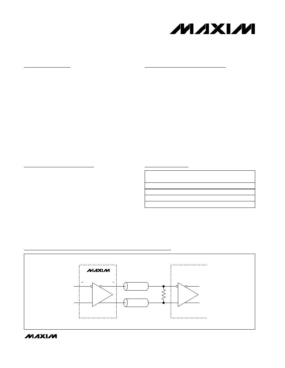
Ordering Information
MAX9374/MAX9374A
LVPECL
INPUT
D
Q
D
Q
Z
0
= 50
Z
0
= 50
100
LVDS RECEIVER
Typical Application Circuit
19-2326; Rev 0; 1/02
For pricing, delivery, and ordering information, please contact Maxim/Dallas Direct! at
1-888-629-4642, or visit Maxim's website at www.maxim-ic.com.
Pin Configurations/Functional Diagrams appear at end of
data sheet.
PART
TEMP
RANGE
PIN-
PACKAGE
TOP
MARK
MAX9374EKA-T
-40
�C to +85�C
8 SOT23-8
AAKU
MAX9374ESA
-40
�C to +85�C
8 SO
--
MAX9374AEKA-T
-40
�C to +85�C
8 SOT23-8
AAKV
MAX9374AESA
-40
�C to +85�C
8 SO
--

MAX9374/MAX9374A
Differential LVPECL-to-LVDS Translators
2
_______________________________________________________________________________________
ABSOLUTE MAXIMUM RATINGS
DC ELECTRICAL CHARACTERISTICS
(V
CC
= 2.375V to 2.625V for MAX9374, V
CC
= 3.0V to 3.6V for MAX9374A, 100
�1% across outputs, V
ID
= 0.095V to V
CC
or 3V,
whichever is less, V
IHD
= 1.2V to V
CC
, V
ILD
= GND to V
CC
- 0.095V, unless otherwise noted. Typical values are at V
IHD
= 2.0V, V
ILD
=
1.85V, V
CC
= 3.3V for MAX9374A, V
CC
= 2.5V for MAX9374.) (Notes 1, 2)
Stresses beyond those listed under "Absolute Maximum Ratings" may cause permanent damage to the device. These are stress ratings only, and functional
operation of the device at these or any other conditions beyond those indicated in the operational sections of the specifications is not implied. Exposure to
absolute maximum rating conditions for extended periods may affect device reliability.
V
CC
to GND...........................................................................4.0V
V
D
, V
D
to GND ..............................................-0.3V to V
CC
+ 0.3V
V
D
to V
D
................................................................................3.0V
V
BB
Sink/Source Current.......................................................1mA
Short-Circuit Duration (Q, Q to GND).........................Continuous
Short-Circuit Duration (Q to Q)...................................Continuous
Continuous Power Dissipation (T
A
= +70�C)
8-Pin SOT23 (derate 8.9mW/�C above +70�C)............714mW
8-Pin SO (derate 5.9mW/�C above +70�C)..................470mW
Junction-to-Ambient Thermal Resistance
8-Pin SOT23.............................................................+112�C/W
8-Pin SO...................................................................+170�C/W
Junction-to-Ambient Thermal Resistance with
500 LFPM Airflow
8-Pin SOT23...............................................................+78�C/W
8-Pin SO.....................................................................+99�C/W
Junction-to-Case Thermal Resistance
8-Pin SOT23...............................................................+80�C/W
8-Pin SO.....................................................................+40�C/W
Operating Temperature Range ...........................-40�C to +85�C
Junction Temperature ......................................................+150�C
Storage Temperature Range .............................-65�C to +150�C
ESD Protection
Human Body Model (D, D, Q, Q) .......................................2kV
Soldering Temperature (10s) ...........................................+300�C
-40�C
+25�C
+85�C
PARAMETER
SYMBOL
CONDITIONS
MIN
TYP
MAX
MIN
TYP
MAX
MIN
TYP
MAX
UNITS
DIFFERENTIAL INPUT (D,
D)
High Voltage of
Differential Input
V
IHD
Figure 1
1.2
V
CC
1.2
V
CC
1.2
V
CC
V
Low Voltage of
Differential Input
V
ILD
Figure 1
GND
V
CC
-
0.095
GND
V
CC
-
0.095
GND
V
CC
-
0.095
V
Single-Ended Input
High Voltage
V
IH
V
BB
connected
to D (V
IL
for
V
BB
connected
to D), Figure 1
V
CC
-
1.165
V
CC
V
CC
-
1.165
V
CC
V
CC
-
1.165
V
CC
V
Single-Ended Input
Low Voltage
V
IL
V
BB
connected
to D (V
IH
for
V
BB
connected
to D), Figure 1
V
EE
V
CC
-
1.475
V
EE
V
CC
-
1.475
V
EE
V
CC
-
1.475
V
V
CC
< 3.0V
0.1
V
CC
0.1
V
CC
0.1
V
CC
Differential Input Voltage
V
IHD
-
V
ILD
V
CC
3.0V
0.1
3.0
0.1
3.0
0.1
3.0
V
Input Current
I
IN
V
IHMAX
, V
ILMIN
(Note 3)
-150
150
-150
150
-150
150
�A
DIFFERENTIAL OUTPUT (Q,
Q)
Output High Voltage
V
OH
Figure 1
1.6
1.6
1.6
V
Output Low Voltage
V
OL
Figure 1
0.9
0.9
0.9
V
Differential Output
Voltage
V
OD
Figure 1
250
350
450
250
350
450
250
350
450
mV
MAX9374/MAX9374A
Differential LVPECL-to-LVDS Translators
_______________________________________________________________________________________
3
DC ELECTRICAL CHARACTERISTICS (continued)
(V
CC
= 2.375V to 2.625V for MAX9374, V
CC
= 3.0V to 3.6V for MAX9374A, 100
�1% across outputs, V
ID
= 0.095V to V
CC
or 3V,
whichever is less, V
IHD
= 1.2V to V
CC
, V
ILD
= GND to V
CC
- 0.095V, unless otherwise noted. Typical values are at V
IHD
= 2.0V, V
ILD
=
1.85V, V
CC
= 3.3V for MAX9374A, V
CC
= 2.5V for MAX9374.) (Notes 1, 2)
-40�C
+25�C
+85�C
PARAMETER
SYMBOL
CONDITIONS
MIN
TYP
MAX
MIN
TYP
MAX
MIN
TYP
MAX
UNITS
Change in V
OD
Between
Complementary Output
States
V
OD
1
25
1
25
1
25
mV
Output Offset Voltage
V
OS
1.125
1.25
1.375 1.125
1.25
1.375 1.125
1.25
1.375
V
Change in V
OS
Between
Complementary Output
States
V
OS
3
25
3
25
3
25
mV
Output Short-Circuit
Current
I
OSC
Q or Q short to
GND
23
30
23
30
23
30
mA
V
BB
AND SUPPLY
Reference Voltage
V
BB
I
BB
= �0.6mA
(Note 4)
V
CC
-
1.38
V
CC
-
1.26
V
CC
-
1.38
V
CC
-
1.26
V
CC
-
1.38
V
CC
-
1.26
V
Supply Current
I
CC
(Note 5)
16
30
18
30
20
30
mA
AC ELECTRICAL CHARACTERISTICS
(V
CC
= 2.375V to 2.625V for MAX9374, V
CC
= 3.0V to 3.6V for MAX9374A, 100
�1% across outputs, V
IHD
- V
ILD
= 0.15V to V
CC
or
3V, whichever is less, V
IHD
= 1.2V to V
CC
, V
ILD
= GND to V
CC
- 0.15V, f
IN
= 1GHz, input transition time = 125ps, input duty cycle =
50%, unless otherwise noted. Typical values are at V
IHD
= 2.0V, V
ILD
= 1.85V, V
CC
= 3.3V for MAX9374A, V
CC
= 2.5V for MAX9374,
unless otherwise noted.) (Notes 1, 6)
-40�C
+25�C
+85�C
PARAMETER
SYMBOL
CONDITIONS
MIN
TYP
MAX
MIN
TYP
MAX
MIN
TYP
MAX
UNITS
Differential Input to
Differential Output Delay
t
PLHD
,
t
PHLD
Figure 1
116
240
420
128
250
403
145
260
440
ps
Single-Ended Input to
Differential Output Delay
t
PLHS
,
t
PHLS
Figure 1
126
250
430
138
250
415
155
260
450
ps
Part-to-Part Skew
t
SKPP
(Note 7)
304
275
295
ps
f
IN
= 1.0GHz,
clock pattern
0.9
2
1
2
1
2
Added Random Jitter
(Note 8)
t
RJ
f
IN
= 2.0GHz,
clock pattern
0.8
2
0.9
2
0.9
2
ps
(RMS)
Added Deterministic
Jitter (Note 8)
t
DJ
f
IN
= 2.0Gbps,
2
23
-1 PRBS
pattern
45
75
46
75
38
75
ps
(P-P)
Operating Frequency
f
MAX
V
OD
250mV
2.0
2.2
2.0
2.2
2.0
2.2
MHz
Output Rise/Fall Time
t
R
, t
F
20% to 80%,
Figure 1
92
200
91
200
90
200
ps

MAX9374/MAX9374A
Differential LVPECL-to-LVDS Translators
4
_______________________________________________________________________________________
Typical Operating Characteristics
(MAX9374A, 100
�1% across outputs, f
IN
= 1GHz, input transition time = 125ps, input duty cycle = 50%, V
CC
= 3.3V, V
IHD
= 2.0V,
V
ILD
= 1.85V, T
A
= +25�C, unless otherwise noted.)
SUPPLY CURRENT vs. TEMPERATURE
MAX9374 toc01
TEMPERATURE (
�C)
SUPPLY CURRENT (mA)
60
35
10
-15
12
14
16
18
20
22
24
10
-40
85
100
LOAD
DIFFERENTIAL OUTPUT VOLTAGE (V
OD
)
vs. FREQUENCY
MAX9374 toc02
FREQUENCY (GHz)
DIFFERENTIAL OUTPUT VOLTAGE (mV)
1.9
1.6
1.3
1.0
0.7
0.4
150
200
250
300
350
400
100
0.1
2.2
JITTER
V
OD
1
2
3
0
RANDOM JITTER (ps
RMS
)
RISE/FALL TIME vs. TEMPERATURE
MAX9374 toc03
TEMPERATURE (
�C)
RISE/FALL TIME (ps)
60
35
10
-15
60
80
100
120
140
40
-40
85
RISE
FALL
PROPAGATION DELAY vs. HIGH VOLTAGE
OF DIFFERENTIAL INPUT (V
IHD
)
MAX9374 toc04
V
IHD
(V)
PROPAGATION DELAY (ps)
3.0
2.7
2.4
2.1
1.8
1.5
200
220
240
260
280
180
1.2
3.3
PROPAGATION DELAY vs. TEMPERATURE
MAX9374 toc05
TEMPERATURE (
�C)
PROPAGATION DELAY (ps)
60
35
10
-15
220
240
260
280
300
200
-40
85
Note 1: Measurements are made with the device in thermal equilibrium.
Note 2: DC parameters are production tested at T
A
= +25�C and guaranteed by design over the full operating temperature range.
Note 3: Current into a pin is defined as positive. Current out of a pin is defined as negative.
Note 4: Use V
BB
as a reference for inputs on the same device only.
Note 5: 100
across the outputs, all other pins open except V
CC
and GND.
Note 6: Guaranteed by design and characterization. Limits are set at �6 sigma.
Note 7: Measured between outputs of different parts at the signal crossing points under identical conditions for a same-edge transition.
Note 8: Device jitter added to the input signal.
AC ELECTRICAL CHARACTERISTICS (continued)
(V
CC
= 2.375V to 2.625V for MAX9374, V
CC
= 3.0V to 3.6V for MAX9374A, 100
�1% across outputs, V
IHD
- V
ILD
= 0.15V to V
CC
or
3V, whichever is less, V
IHD
= 1.2V to V
CC
, V
ILD
= GND to V
CC
- 0.15V, f
IN
= 1GHz, input transition time = 125ps, input duty cycle =
50%, unless otherwise noted. Typical values are at V
IHD
= 2.0V, V
ILD
= 1.85V, V
CC
= 3.3V for MAX9374A, V
CC
= 2.5V for MAX9374,
unless otherwise noted.) (Notes 1, 6)

MAX9374/MAX9374A
Differential LVPECL-to-LVDS Translators
_______________________________________________________________________________________
5
Pin Description
PIN
SOT23
SO
NAME
FUNCTION
1
4
V
BB
Reference Output Voltage. Connect to the inverting or noninverting data input to provide a reference
for single-ended operation. When used, bypass with a 0.01�F ceramic capacitor to V
CC
; otherwise,
leave it open.
2
5
GND
Ground. Provide a low-impedance connection to the ground plane.
3
3
D
Inverted LVPECL Data Input. 36.5k
pullup to V
CC
and 75k
pulldown to GND.
4
2
D
Noninverted LVPECL Data Input. 75k
pullup to V
CC
and 75k
pulldown to GND.
5
8
V
CC
Positive Supply Voltage. Bypass V
CC
to GND with 0.1�F and 0.01�F ceramic capacitors. Place the
capacitors as close to the device as possible with the smaller value capacitor closest to the device.
6
7
Q
Noninverted LVDS Output. Typically terminate with 100
to Q.
7
6
Q
Inverted LVDS Output. Typically terminate with 100
to Q.
8
1
N.C.
No Connection. Not internally connected.
V
IHD
- V
ILD
D
D
V
IHD
V
ILD
V
OD
V
OS
Q
Q
V
OH
V
OL
t
PLH_
t
PHL_
t
R
(Q) - (Q)
20%
80%
t
F
80%
20%
0 (DIFFERENTIAL)
0 (DIFFERENTIAL)
Figure 1. MAX9374/MAX9374A Timing Diagram