 | ÐлекÑÑоннÑй компоненÑ: MAX9389 | СкаÑаÑÑ:  PDF PDF  ZIP ZIP |
Äîêóìåíòàöèÿ è îïèñàíèÿ www.docs.chipfind.ru
General Description
The MAX9389 is a fully differential, high-speed, low-jitter,
8-to-1 ECL/PECL multiplexer (mux) with dual output
buffers. The device is designed for clock and data distri-
bution applications, and features extremely low propa-
gation delay (310ps typ) and output-to-output skew
(30ps max).
Three single-ended select inputs, SEL0, SEL1, and SEL2,
control the mux function. The mux select inputs are com-
patible with ECL/PECL logic, and are internally refer-
enced to the on-chip reference output (V
BB1
, V
BB2
),
nominally V
CC
- 1.425V. The select inputs accept signals
between V
CC
and V
EE
. Internal pulldowns to V
EE
ensure
a low default condition if the select inputs are left open.
The differential inputs D_, D_ can be configured to
accept a single-ended signal when the unused comple-
mentary input is connected to the on-chip reference
output (V
BB1
, V
BB2
). All the differential inputs have
internal bias and clamping circuits that ensure a low
output state when the inputs are left open.
The MAX9389 operates with a wide supply range V
CC
-
V
EE
of 2.375V to 5.5V. The device is offered in 32-pin
TQFP and thin QFN packages, and operates over the
-40°C to +85°C extended temperature range.
Applications
High-Speed Telecom and Datacom Applications
Central-Office Backplane Clock Distribution
DSLAM/DLC
Features
o 310ps Propagation Delay
o Guaranteed 2.7GHz Operating Frequency
o 0.3ps
RMS
Random Jitter
o <30ps Output-to-Output Skew
o -2.375V to -5.5V Supplies for Differential
LVECL/ECL
o +2.375V to +5.5V Supplies for Differential
LVPECL/PECL
o Outputs Low for Open Inputs
o Dual Output Buffers
o >2kV ESD Protection (Human Body Model)
MAX9389
Differential 8:1 ECL/PECL Multiplexer with
Dual Output Buffers
________________________________________________________________ Maxim Integrated Products
1
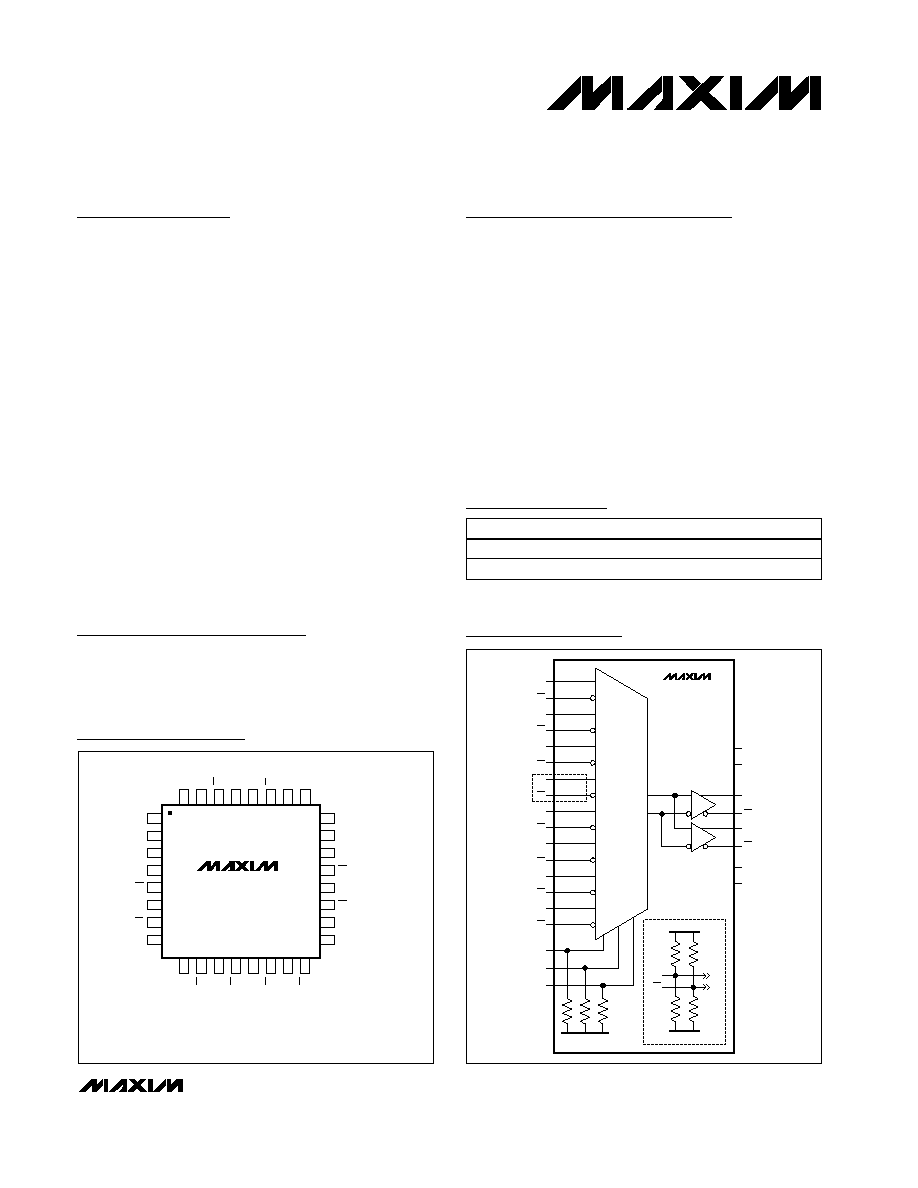
MAX9389
TQFP
TOP VIEW
32
28
29
30
31
25
26
27
Q0
Q0
V
CC
Q1
V
EE
Q1
V
CC
SEL2
10
13
15
14
16
11
12
9
D2
D3
D2
D4
D3
D5
D4
D5
17
18
19
20
21
22
23 SEL0
24 SEL1
V
CC
D7
D7
D6
D6
V
EE
2
3
4
5
6
7
8
V
CC
D1
D1
D0
D0
V
BB1
V
BB2
1
V
CC
Pin Configurations
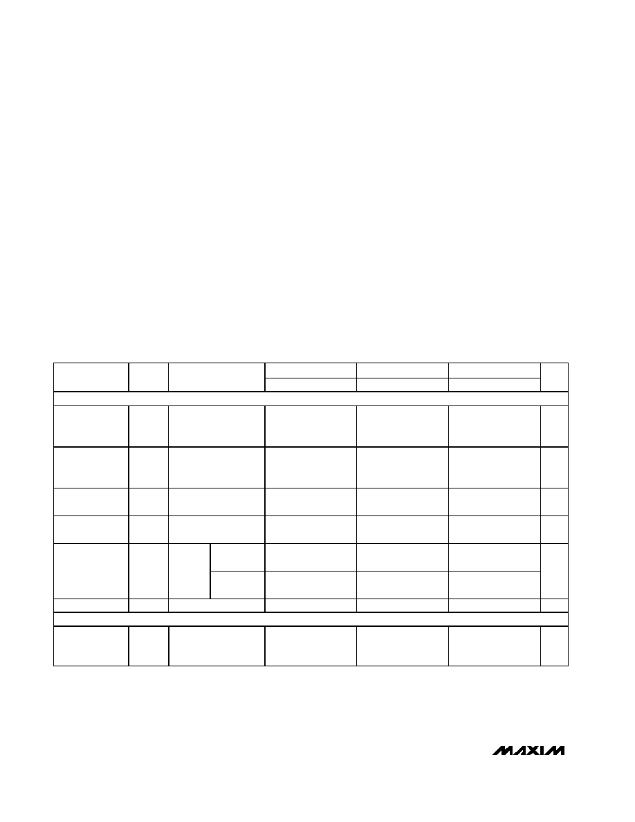
Ordering Information
V
BB1
V
BB2
V
CC
V
EE
V
CC
V
EE
MUX
8:1
180k
180k
165k
180k
232k
D0
D0
D1
D1
D2
D2
D3
D3
D4
SEL0
SEL1
SEL2
D4
Q0
Q0
Q1
Q1
D_
D_
MAX9389
V
EE
D5
D5
D6
D6
D7
D7
Functional Diagram
19-2688; Rev 0; 1/03
For pricing, delivery, and ordering information, please contact Maxim/Dallas Direct! at
1-888-629-4642, or visit Maxim's website at www.maxim-ic.com.
PART
TEMP RANGE
PIN-PACKAGE
MAX9389EHJ
-40
°C to +85°C
32 TQFP
MAX9389ETJ*
-40
°C to +85°C
32 Thin QFN
Pin Configurations continued at end of data sheet.
*Future product--contact factory for availability.
MAX9389
Differential 8:1 ECL/PECL Multiplexer with
Dual Output Buffers
2
_______________________________________________________________________________________
ABSOLUTE MAXIMUM RATINGS
DC ELECTRICAL CHARACTERISTICS
(V
CC
- V
EE
= 2.375V to 5.5V, outputs loaded with 50
±1% to V
CC
- 2V. Typical values are at V
CC
- V
EE
= 3.3V, V
IHD
= V
CC
- 1V,
V
ILD
= V
CC
- 1.5V, unless otherwise noted.) (Notes 14)
Stresses beyond those listed under "Absolute Maximum Ratings" may cause permanent damage to the device. These are stress ratings only, and functional
operation of the device at these or any other conditions beyond those indicated in the operational sections of the specifications is not implied. Exposure to
absolute maximum rating conditions for extended periods may affect device reliability.
V
CC
- V
EE
..............................................................-0.3V to +6.0V
Inputs (D_, D_, SEL_) to V
EE
......................-0.3V to (V
CC
+ 0.3V)
D_ to D_...............................................................................
±3.0V
Continuous Output Current .................................................50mA
Surge Output Current........................................................100mA
V
BB
_ Sink/Source Current ..............................................±600µA
Continuous Power Dissipation (T
A
= +70°C)
32-Lead TQFP (derate 13.1mW/°C above +70°C) ...1047mW
JA
in Still Air..........................................................+76°C/W
JC
.........................................................................+25°C/W
32-Lead QFN (derate 21.3mW/°C above +70°C) .....1702mW
JA
in Still Air..........................................................+47°C/W
JC
...........................................................................+2°C/W
Operating Temperature Range ...........................-40
°C to +85°C
Junction Temperature ......................................................+150°C
Storage Temperature Range .............................-65°C to +150°C
ESD Protection
Human Body Model (D_, D_, Q_, Q_, SEL_, V
BB
_) .............
2kV
Soldering Temperature (10s) ...........................................+300°C
-40
°C
+25
°C
+85
°C
PARAMETER
SYMBOL
CONDITIONS
MIN
TYP
MAX
MIN
TYP
MAX
MIN
TYP
MAX
UNITS
INPUT (D_,
D_, SEL_)
Single-Ended
Input High
Voltage
V
IH
V
BB_
connected to the
unused input, Figure 1
V
CC
-
1.225
V
CC
-
0.880
V
CC
-
1.225
V
CC
-
0.880
V
CC
-
1.225
V
CC
-
0.880
V
Single-Ended
Input Low
Voltage
V
IL
V
BB_
connected to the
unused input, Figure 1
V
CC
-
1.945
V
CC
-
1.625
V
CC
-
1.945
V
CC
-
1.625
V
CC
-
1.945
V
CC
-
1.625
V
Differential Input
High Voltage
V
IHD
Figure 1
V
EE
+
1.2
V
CC
V
EE
+
1.2
V
CC
V
EE
+
1.2
V
CC
V
Differential Input
Low Voltage
V
ILD
Figure 1
V
EE
V
CC
-
0.095
V
EE
V
CC
-
0.095
V
EE
V
CC
-
0.095
V
V
CC
- V
EE
<
3.0V
0.095
V
CC
-
V
EE
0.095
V
CC
-
V
EE
0.095
V
CC
-
V
EE
Differential Input
Voltage
V
IHD
-
V
ILD
Figure 1
V
CC
- V
EE
3.0V
0.095
3.000
0.095
3.000
0.095
3.000
V
Input Current
I
IN
V
IH,
V
IL,
V
IHD,
V
ILD
-60
+60
-60
+60
-60
+60
µA
OUTPUT (Q_,
Q_)
Single-Ended
Output High
Voltage
V
OH
Figure 2
V
CC
-
1.145
V
CC
-
0.895
V
CC
-
1.145
V
CC
-
0.895
V
CC
-
1.145
V
CC
-
0.895
V
MAX9389
Differential 8:1 ECL/PECL Multiplexer with
Dual Output Buffers
_______________________________________________________________________________________
3
DC ELECTRICAL CHARACTERISTICS (continued)
(V
CC
- V
EE
= 2.375V to 5.5V, outputs loaded with 50
±1% to V
CC
- 2V. Typical values are at V
CC
- V
EE
= 3.3V, V
IHD
= V
CC
- 1V,
V
ILD
= V
CC
- 1.5V, unless otherwise noted.) (Notes 14)
-40
°C
+25
°C
+85
°C
PARAMETER
SYMBOL
CONDITIONS
MIN
TYP
MAX
MIN
TYP
MAX
MIN
TYP
MAX
UNITS
Single-Ended
Output Low
Voltage
V
OL
Figure 2
V
CC
-
1.945
V
CC
-
1.695
V
CC
-
1.945
V
CC
-
1.695
V
CC
-
1.945
V
CC
-
1.695
V
Differential
Output Voltage
V
OH
-
V
OL
Figure 2
650
830
650
840
650
840
mV
REFERENCE OUTPUT (V
BB
_
)
Reference
Voltage Output
V
BB1
V
BB2
I
BB1
+ I
BB2
=
±0.5mA
(Note 5)
V
CC
-
1.525
V
CC
-
1.425
V
CC
-
1.325
V
CC
-
1.525
V
CC
-
1.425
V
CC
-
1.325
V
CC
-
1.525
V
CC
-
1.425
V
CC
-
1.325
V
POWER SUPPLY
Supply Current
I
EE
(Note 6)
50
70
53
70
55
70
mA
AC ELECTRICAL CHARACTERISTICS
(V
CC
- V
EE
= 2.375V to 5.5V, outputs loaded with 50
±1% to V
CC
- 2V, V
IHD
- V
ILD
= 0.15V to 1V, f
IN
2.5GHz, input duty cycle = 50%,
input transition time = 125ps (20% to 80%). Typical values are at V
CC
- V
EE
= 3.3V, V
IHD
= V
CC
- 1V, V
ILD
= V
CC
- 1.5V, f
IN
= 622 MHz,
input duty cycle = 50%, input transition time = 125ps (20% to 80%.)) (Note 7)
-40
°C
+25
°C
+85
°C
PARAMETER
SYMBOL
CONDITIONS
MIN
TYP
MAX
MIN
TYP
MAX
MIN
TYP
MAX
UNITS
Differential Input-
to-Output Delay
t
PLHD
,
t
PHLD
Figure 2
216
301
370
237
310
416
255
329
456
ps
SEL_-to-Output
Delay
t
PLH2
,
t
PHL2
Figure 4, input
transition time = 500ps
(20% to 80%) (Note 8)
1.34
2
1.25
2
1.44
2
ns
Output-to-Output
Skew
t
SKOO
Figure 5 (Note 9)
15
15
30
ps
Input-to-Output
Skew
t
SKIO
Figure 6 (Note 10)
50
50
55
ps
Part-to-Part
Skew
t
SKPP
(Note 11)
125
150
160
ps
f
IN
= 156MHz
0.3
1.15
0.3
1.15
0.3
1.15
f
IN
= 622MHz
0.3
1.15
0.3
1.15
0.3
1.15
Added Random
Jitter (Note 12)
t
RJ
Clock
pattern
f
IN
= 2.5GHz
0.3
1.15
0.3
1.15
0.3
1.15
ps
RMS
f
IN
= 156Mbps
33
95
33
95
33
95
Added
Deterministic
Jitter (Note 12)
T
DJ
PRBS
2
23
- 1
f
IN
= 622Mbps
21
61
21
61
21
61
ps
P-P
MAX9389
Differential 8:1 ECL/PECL Multiplexer with
Dual Output Buffers
4
_______________________________________________________________________________________
AC ELECTRICAL CHARACTERISTICS (continued)
(V
CC
- V
EE
= 2.375V to 5.5V, outputs loaded with 50
±1% to V
CC
- 2V, V
IHD
- V
ILD
= 0.15V to 1V, f
IN
2.5GHz, input duty cycle = 50%,
input transition time = 125ps (20% to 80%). Typical values are at V
CC
- V
EE
= 3.3V, V
IHD
= V
CC
- 1V, V
ILD
= V
CC
- 1.5V, f
IN
= 622 MHz,
input duty cycle = 50%, input transition time = 125ps (20% to 80%.)) (Note 7)
-40
°C
+25
°C
+85
°C
PARAMETER
SYMBOL
CONDITIONS
MIN
TYP
MAX
MIN
TYP
MAX
MIN
TYP
MAX
UNITS
Switching
Frequency
f
MAX
V
OH
- V
OL
300mV,
Figure 2
2.7
2.7
2.7
GHz
Select Toggle
Frequency
f
SEL
V
OH
- V
OL
300mV,
Figure 4
100
100
100
MHz
Output Rise and
Fall Time
(20% to 80%)
t
R
, t
F
Figure 2
67
105
138
74
117
155
81
128
165
ps
Note 1: Measurements are made with the device in thermal equilibrium.
Note 2: Current into an I/O pin is defined as positive. Current out of an I/O pin is defined as negative.
Note 3: DC parameters production tested at T
A
= +25
°C and guaranteed by design over the full operating temperature range.
Note 4: Single-ended data input operation using V
BB
_ is limited to (V
CC
- V
EE
)
3.0V.
Note 5: Use V
BB_
only for inputs that are on the same device as the V
BB_
reference.
Note 6: All pins open except V
CC
and V
EE
.
Note 7: Guaranteed by design and characterization. Limits are set at
±6 sigma.
Note 8: Measured from the 50% point of the input signal with the 50% point equal to V
BB
, to the 50% point of the output signal.
Note 9: Measured between outputs of the same part at the signal crossing points for a same-edge transition.
Note 10: Measured between input-to-output paths of the same part at the signal crossing points for a same-edge transition of the
differential input signal.
Note 11: Measured between outputs of different parts at the signal crossing points under identical conditions for a same-edge
transition.
Note 12: Device jitter added to the differential input signal.
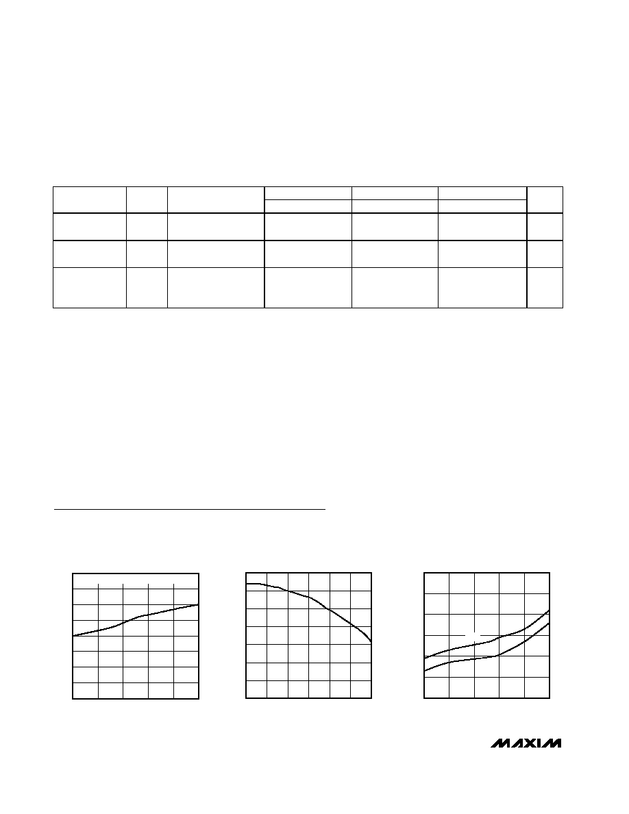
SUPPLY CURRENT vs. TEMPERATURE
MAX9389 toc01
TEMPERATURE (
°C)
SUPPLY CURRENT (mA)
60
35
-15
10
42.5
45.0
47.5
50.0
52.5
55.0
57.5
60.0
40.0
-40
85
ALL PINS ARE OPEN EXCEPT V
CC
AND V
EE
DIFFERENTIAL OUTPUT VOLTAGE (V
OH
- V
OL
)
vs. FREQUENCY
MAX9389 toc02
FREQUENCY (GHz)
DIFFERENTIAL OUTPUT VOLTAGE (mV)
2.5
2.0
1.5
1.0
0.5
300
400
500
600
700
800
900
200
0
3.0
OUTPUT RISE/FALL TIME
vs. TEMPERATURE
MAX9389 toc03
RISE/FALL TIME (ps)
100
110
120
130
140
150
90
TEMPERATURE (
°C)
60
35
10
-15
-40
RISE
FALL
85
Typical Operating Characteristics
(V
CC
- V
EE
= 3.3V, V
IHD
= V
CC
- 1V, V
ILD
= V
CC
- 1.5V, outputs loaded with 50
±1% to V
CC
- 2V, f
IN
= 622MHz, input duty cycle = 50%,
input transition time = 125ps (20% to 80%), unless otherwise noted.)
MAX9389
Differential 8:1 ECL/PECL Multiplexer with
Dual Output Buffers
_______________________________________________________________________________________
5
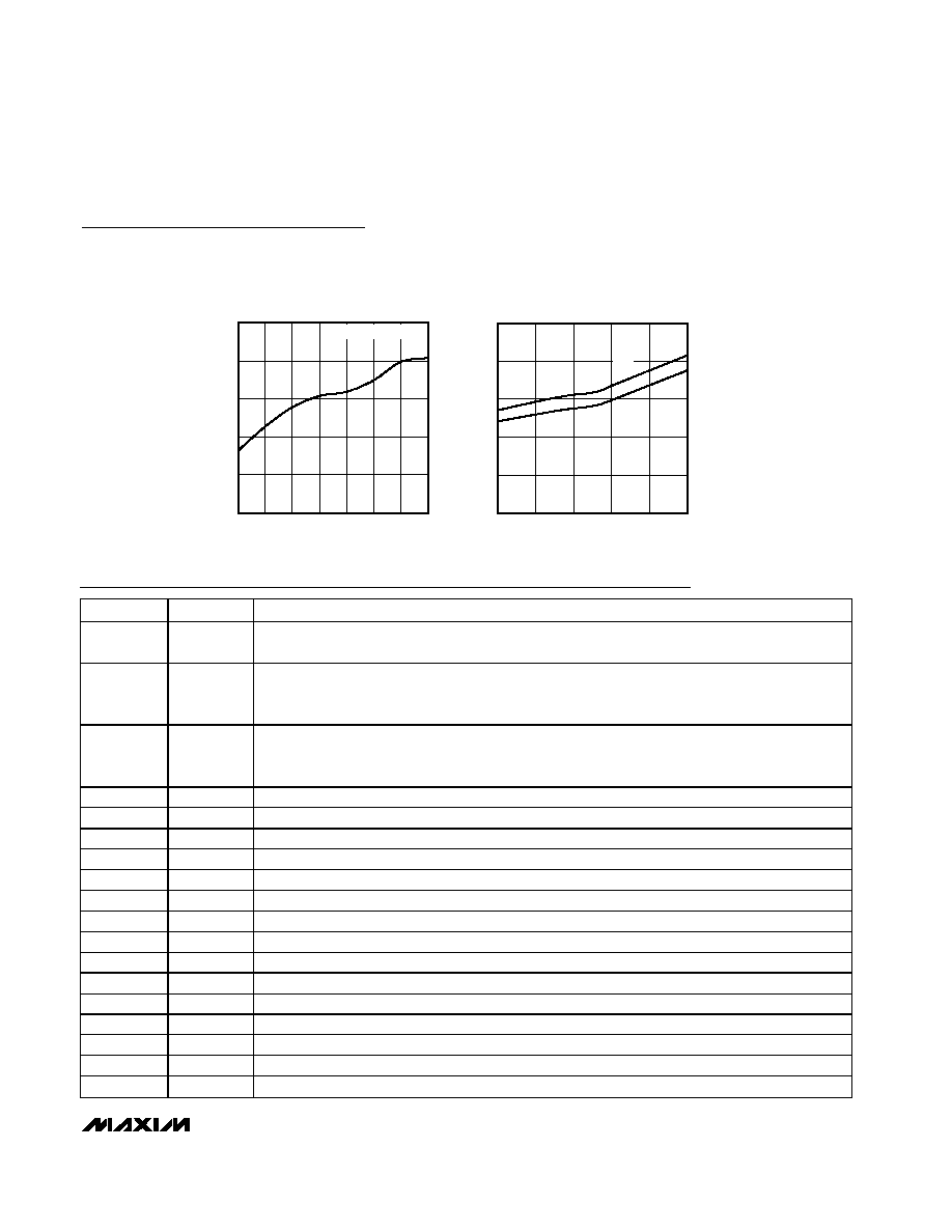
PROPAGATION DELAY vs. HIGH VOLTAGE
OF DIFFERENTIAL INPUT (V
IHD
)
MAX9389 toc04
V
IHD
(V)
PROPAGATION DELAY (ps)
3.0
2.7
2.4
2.1
1.8
1.5
276
292
308
324
340
260
1.2
3.3
V
IHD
- V
ILD
= 150mV
PROPAGATION DELAY vs. TEMPERATURE
MAX9389 toc05
TEMPERATURE (
°C)
PROPAGATION DELAY (ps)
60
35
10
-15
270
290
310
330
350
250
-40
t
PHL
t
PLH
85
Typical Operating Characteristics (continued)
(V
CC
- V
EE
= 3.3V, V
IHD
= V
CC
- 1V, V
ILD
= V
CC
- 1.5V, outputs loaded with 50
±1% to V
CC
- 2V, f
IN
= 622MHz, input duty cycle = 50%,
input transition time = 125ps (20% to 80%), unless otherwise noted.)
Pin Description
PIN
NAME
FUNCTION
1, 8, 22,
26, 29
V
CC
Positive Supply Input. Bypass each V
CC
to V
EE
with 0.1µF and 0.01µF ceramic capacitors. Place the
capacitors as close to the device as possible with the smaller value capacitor closest to the device.
2
V
BB2
Reference Output Voltage 2. Connect to the inverting or noninverting data input to provide a
reference for single-ended operation. When used, bypass V
BB2
to V
CC
with a 0.01µF ceramic
capacitor. Otherwise leave open.
3
V
BB1
Reference Output Voltage 1. Connect to the inverting or noninverting data input to provide a
reference for single-ended operation. When used, bypass V
BB1
to V
CC
with a 0.01µF ceramic
capacitor. Otherwise leave open.
4
D0
Noninverting Differential Input 0. Internal 232k
to V
CC
and 180k
to V
EE
.
5
D0
Inverting Differential Input 0. Internal 180k
to V
CC
and 180k
to V
EE
.
6
D1
Noninverting Differential Input 1. Internal 232k
to V
CC
and 180k
to V
EE
.
7
D1
Inverting Differential Input 1. Internal 180k
to V
CC
and 180k
to V
EE
.
9
D2
Noninverting Differential Input 2. Internal 232k
to V
CC
and 180k
to V
EE
.
10
D2
Inverting Differential Input 2. Internal 180k
to V
CC
and 180k
to V
EE
.
11
D3
Noninverting Differential Input 3. Internal 232k
to V
CC
and 180k
to V
EE
.
12
D3
Inverting Differential Input 3. Internal 180k
to V
CC
and 180k
to V
EE
.
13
D4
Noninverting Differential Input 4. Internal 232k
to V
CC
and 180k
to V
EE
.
14
D4
Inverting Differential Input 4. Internal 180k
to V
CC
and 180k
to V
EE
.
15
D5
Noninverting Differential Input 5. Internal 232k
to V
CC
and 180k
to V
EE
.
16
D5
Inverting Differential Input 5. Internal 180k
to V
CC
and 180k
to V
EE
.
17, 32
V
EE
Negative Supply Input
18
D6
Noninverting Differential Input 6. Internal 232k
to V
CC
and 180k
to V
EE
.
19
D6
Inverting Differential Input 6. Internal 180k
to V
CC
and 180k
to V
EE
.