 | ÐлекÑÑоннÑй компоненÑ: MAX9425 | СкаÑаÑÑ:  PDF PDF  ZIP ZIP |
Äîêóìåíòàöèÿ è îïèñàíèÿ www.docs.chipfind.ru
General Description
The MAX9424MAX9427 high-speed, low-skew quad
PECL-to-ECL translators are designed for high-speed
data and clock driver applications. These devices feature
an ultra-low 0.24ps
(RMS)
random jitter and channel-to-
channel skew is less than 90ps in asynchronous mode.
The four channels can be operated synchronously with
an external clock, or in asynchronous mode determined
by the state of the SEL input. An enable input provides
the ability to force all the outputs to a differential low state.
The parts differ from one another by their input and out-
put termination options. The input options are an open
input or an internal differential 100
termination. The
output options are an open-emitter output or a series
50
termination. See Ordering Information.
The MAX9424MAX9427 operate from a positive voltage
supply of +2.375V to +5.5V, and a negative supply volt-
age of -2.375V to -5.5V and operate across the extended
temperature range of -40°C to +85°C. They are offered in
32-pin 5mm x 5mm TQFP and space-saving 5mm x 5mm
QFN packages.
Applications
Data and Clock Driver and Buffer
Central Office Backplane Clock Distribution
DSLAM Backplane
Base Station
ATE
Features
o 0.24ps RMS Added Random Jitter
o 10ps Channel-to-Channel Skew in Synchronous
Mode
o Guaranteed 500mV Differential Output at 3GHz
Clock Frequency
o 420ps Propagation Delay in Asynchronous Mode
o Functionally Compatible with
SK4426 (MAX9424)
SK4430 (MAX9425)
SK4436 (MAX9426)
SK4440 (MAX9427)
o Integrated 50 Outputs (MAX9425/MAX9427)
o Integrated 100 Inputs (MAX9426/MAX9427)
o Synchronous/Asynchronous Operation
MAX9424MAX9427
Lowest Jitter Quad PECL-to-ECL
Differential Translators
________________________________________________________________ Maxim Integrated Products
1
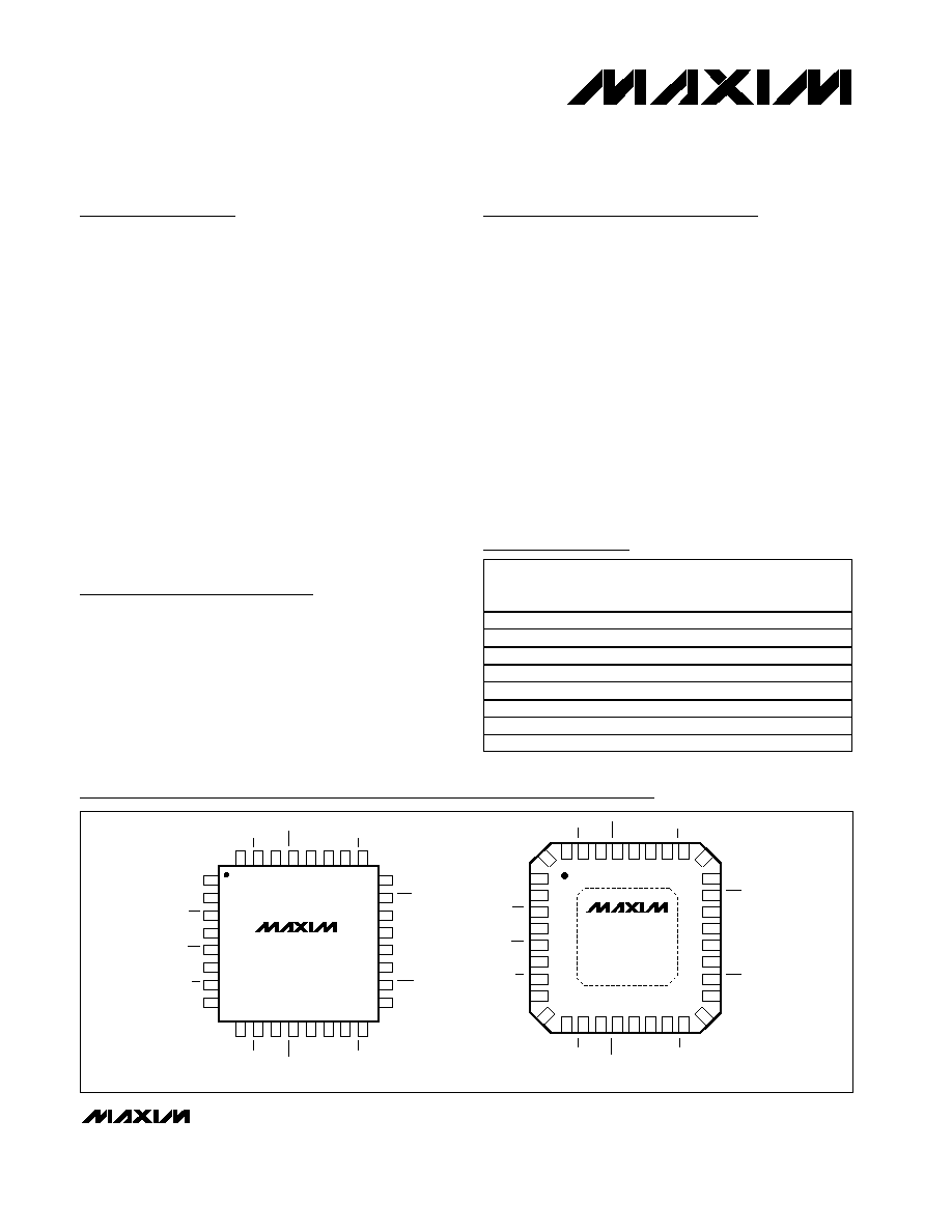
MAX9424
MAX9425
MAX9426
MAX9427
TQFP (5mm x 5mm)
TOP VIEW
32
28
29
30
31
25
26
27
IN0
V
GG
OUT0
OUT0
IN0
V
EE
IN1
IN1
10
13
15
14
16
11
12
9
IN3
V
GG
OUT3
IN2
V
EE
17
18
19
20
21
22
23 OUT1
24 V
GG
OUT1
V
EE
V
EE
OUT2
OUT2
V
GG
2
3
4
5
6
7
8
V
CC
EN
CLK
SEL
1
V
CC
SEL
CLK
EN
IN3
OUT3
IN2
32
31
30
29
28
27
26
IN0
IN0
V
GG
OUT0
OUT0
V
EE
IN1
25
IN1
9
10
11
12
13
14
15
IN3
IN3
V
GG
OUT3
OUT3
V
EE
IN2
16
IN2
17
18
19
20
21
22
23
V
GG
NOTE: CORNER PINS ARE CONNECTED TO V
GG
.
OUT2
OUT2
V
EE
V
EE
OUT1
OUT1
8
7
6
5
4
3
2
V
CC
EN
EN
CLK
CLK
SEL
SEL
MAX9424
MAX9425
MAX9426
MAX9427
QFN
1
V
CC
24
V
GG
TOP VIEW
*
*
*
*
Pin Configurations
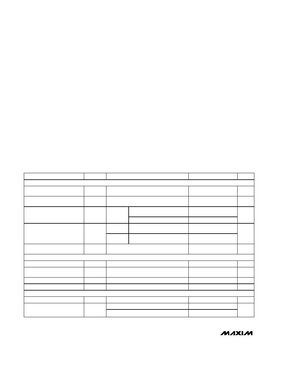
Ordering Information
19-2390; Rev 0; 4/02
For pricing, delivery, and ordering information, please contact Maxim/Dallas Direct! at
1-888-629-4642, or visit Maxim's website at www.maxim-ic.com.
*Future product--contact factory for availability.
PART
TEMP
RANGE
PIN-
PACKAGE
INPUT
(IN_,
IN_)
OUTPUT
(OUT_,
OUT_)
MAX9424EHJ -40°C to +85°C 32 TQFP
Open
Open
MAX9424EGJ* -40°C to +85°C 32 QFN
Open
Open
MAX9425EHJ -40°C to +85°C 32 TQFP
Open
50
MAX9425EGJ* -40°C to +85°C 32 QFN
Open
50
MAX9426EHJ -40°C to +85°C 32 TQFP
100
Open
MAX9426EGJ* -40°C to +85°C 32 QFN
100
Open
MAX9427EHJ -40°C to +85°C 32 TQFP
100
50
MAX9427EGJ* -40°C to +85°C 32 QFN
100
50
MAX9424MAX9427
Lowest Jitter Quad PECL-to-ECL
Differential Translators
2
_______________________________________________________________________________________
ABSOLUTE MAXIMUM RATINGS
DC ELECTRICAL CHARACTERISTICS
(V
CC
- V
GG
= 2.375V to 5.5V, V
GG
- V
EE
= 2.375V to 5.5V, MAX9424/MAX9426 outputs terminated with 50
to V
GG
- 2.0V,
MAX9425/MAX9427 not externally terminated, T
A
= -40°C to +85°C. Typical values are at V
CC
- V
GG
= 3.3V, V
GG
- V
EE
= 3.3V, V
IHD
= V
CC
- 0.9V, V
ILD
= V
CC
- 1.7V, T
A
= +25°C, unless otherwise noted.) (Notes 1, 2, and 3)
Stresses beyond those listed under "Absolute Maximum Ratings" may cause permanent damage to the device. These are stress ratings only, and functional
operation of the device at these or any other conditions beyond those indicated in the operational sections of the specifications is not implied. Exposure to
absolute maximum rating conditions for extended periods may affect device reliability.
V
CC
to V
GG
............................................................-0.3V to +6.0V
V
GG
to V
EE
.............................................................-0.3V to +6.0V
Input Pins to V
GG
........................................-0.3V to (V
CC
+ 0.3V)
Differential Input Voltage ..............................|V
CC
- V
GG
| or 3.0V,
whichever is less
Continuous Output Current .................................................50mA
Surge Output Current........................................................100mA
Continuous Power Dissipation (T
A
= +70°C)
32-Pin 5mm x 5mm TQFP
(derate 9.5mW/°C above +70°C) .................................761mW
32-Pin 5mm x 5mm QFN
(derate 21.3mW/°C above +70°C) ...................................1.7W
Junction-to-Ambient Thermal Resistance in Still Air
32-Pin 5mm x 5mm TQFP ........................................+105°C/W
32-Pin 5mm x 5mm QFN............................................+47°C/W
Junction-to-Ambient Thermal Resistance with
500LFPM Airflow
32-Pin 5mm x 5mm TQFP ..........................................+73°C/W
Junction-to-Case Thermal Resistance
32-Pin 5mm x 5mm TQFP ..........................................+25°C/W
32-Pin 5mm x 5mm QFN..............................................+2°C/W
Operating Temperature Range ...........................-40
°C to +85°C
Junction Temperature ......................................................+150°C
Storage Temperature Range .............................-65
°C to +150°C
ESD Protection
Human Body Model (all input pins) ...............................±500V
Human Body Model (all output pins) ...............................±2kV
Soldering Temperature (10s) ...........................................+300°C
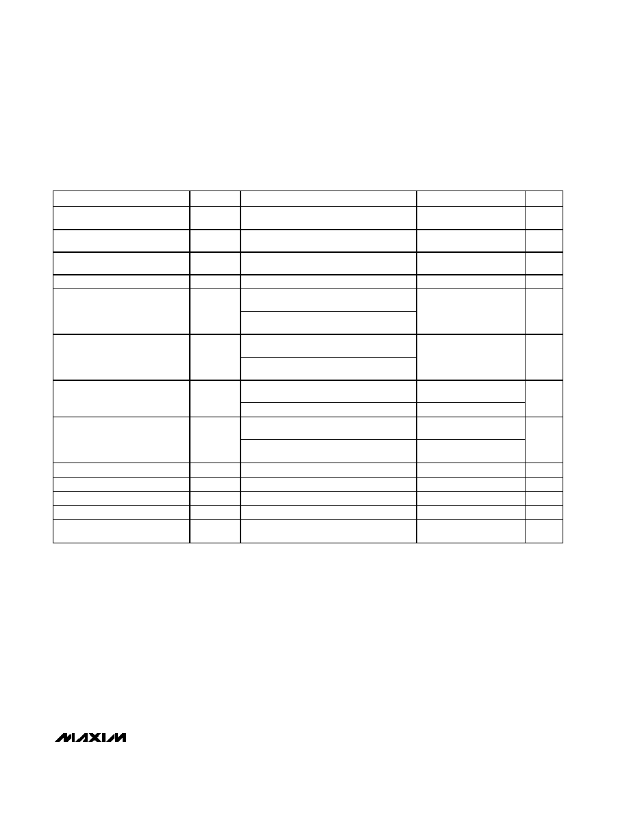
PARAMETER
SYMBOL
CONDITIONS
MIN
TYP
MAX
UNITS
INPUTS (IN_,
IN_, CLK, CLK, EN, EN, SEL, SEL)
Differential Input High Voltage
V
IHD
Figure 1
V
GG
+
1.4
V
CC
V
Differential Input Low Voltage
V
ILD
Figure 1
V
GG
V
CC
-
0.2
V
V
CC
- V
GG
< 3.0V
0.2
V
CC
-
V
GG
Differential Input Voltage
V
ID
Figure 1
V
CC
- V
GG
3.0V
0.2
3.0
V
MAX9424/
MAX9425
EN,
EN, SEL, SEL, IN_, IN_, CLK
or
CLK = V
IHD
or V
ILD
-10
25
Input Current
I
IH
, I
IL
MAX9426/
MAX9427
EN,
EN, SEL, SEL, CLK, or CLK
= V
IHD
or V
ILD
-10
25
µA
Differential Input Resistance
(IN_,
IN_)
R
IN
MAX9426/MAX9427
86
100
114
OUTPUTS (OUT_,
OUT_)
Differential Output Voltage
V
OH
- V
OL
Figure 1
600
635
mV
Output Common-Mode Voltage
V
OCM
Figure 1
V
GG
-
1.50
V
GG
-
1.25
V
GG
-
1.05
V
Output Impedance
R
OUT
MAX9425/MAX9427
40
50
60
Internal Current Source
I
SINK
MAX9425/MAX9427
6
8
10
mA
POWER SUPPLY
Positive Supply Current
I
CC
(Note 4)
16
27
mA
MAX9424/MAX9426 (Note 4)
100
130
Negative Supply Current
I
EE
MAX9425/MAX9427 (Note 4)
172
230
mA
MAX9424MAX9427
Lowest Jitter Quad PECL-to-ECL
Differential Translators
_______________________________________________________________________________________
3
AC ELECTRICAL CHARACTERISTICS
(V
CC
- V
GG
= 2.375V to 5.5V, V
GG
- V
EE
= 2.375V to 5.5V, outputs terminated with 50
to V
GG
- 2.0V, EN = V
IHD
, EN = V
ILD
, f
CLK
3.0GHz, f
IN
1.5GHz, input transition time = 125ps (20% to 80%), V
IHD
= V
GG
+ 1.4V to V
CC
, V
ILD
= V
GG
to V
CC
- 0.2V, V
IHD
- V
ILD
= 0.2V to smallest of |V
CC
- V
GG
| or 3.0V, T
A
= -40°C to +85°C, unless otherwise noted. Typical values are at V
CC
- V
GG
= 3.3V, V
GG
- V
EE
= 3.3V, V
IHD
= V
CC
- 0.9V, V
ILD
= V
CC
- 1.7V, T
A
= +25°C, unless otherwise noted.) (Notes 1 and 5)
PARAMETER
SYMBOL
CONDITIONS
MIN
TYP
MAX
UNITS
IN_ to OUT_ Differential
Propagation Delay
t
PLH1
t
PHL1
Figure 3, SEL = high, asynchronous
operation
300
420
570
ps
CLK to OUT_ Differential
Propagation Delay
t
PLH2
t
PHL2
Figure 4, SEL = low, synchronous operation
460
580
730
ps
OUT_ to OUT_ Skew
t
SKD1
SEL = high, asynchronous operation
(Note 6)
38
90
ps
OUT_ to OUT_ Skew
t
SKD2
SEL = low, synchronous operation (Note 6)
10
70
ps
MAX9424/MAX9426, V
OH
- V
OL
500mV,
SEL = low
Maximum Clock Frequency
f
CLK(MAX)
MAX9425/MAX9427, V
OH
- V
OL
300mV,
SEL = low
3.0
GHz
MAX9424/MAX9426, V
OH
- V
OL
400mV,
SEL = high
Maximum Data Frequency
f
IN(MAX)
MAX9425/MAX9427, V
OH
- V
OL
250mV,
SEL = high
2.0
GHz
SEL = low, f
CLK
= 3.0GHz clock, f
IN
=
1.5GHz (Note 7)
0.24
0.8
Added Random Jitter
t
RJ
SEL = high, f
IN
= 2.0GHz (Note 7)
0.3
0.8
ps
(RMS)
SEL = low, f
CLK
= 3.0GHz, IN_ = 3.0Gbps
2
23
- 1 PRBS pattern (Note 7)
27
80
Added Deterministic Jitter
t
DJ
SEL = high, IN_ = 2.0Gbps 2
23
- 1 PRBS
pattern (Note 7)
20
80
ps
(P-P)
IN_ to CLK Setup Time
t
S
Figure 4
80
ps
CLK to IN_ Hold Time
t
H
Figure 4
80
ps
Output Rise Time
t
R
Figure 3
89
120
ps
Output Fall Time
t
F
Figure 3
87
120
ps
Propagation Delay Temperature
Coefficient
t
PD
/
T
0.2
1
ps/°C
Note 1: Measurements are made with the device in thermal equilibrium.
Note 2: Current into a pin is defined as positive. Current out of a pin is defined as negative.
Note 3: DC parameters are production tested at +25°C. DC limits are guaranteed by design and characterization over the full
operating temperature range.
Note 4: All outputs open, all inputs biased differential high or low except V
CC
, V
GG
, and V
EE
.
Note 5: Guaranteed by design and characterization, and are not production tested. Limits are set to ±6 sigma.
Note 6: Measured between outputs of the same part at the signal crossing points for a same-edge transition.
Note 7: Device jitter added to the input signal.
MAX9424MAX9427
Lowest Jitter Quad PECL-to-ECL
Differential Translators
4
_______________________________________________________________________________________
Typical Operating Characteristics
(MAX9424: V
CC
- V
GG
= 3.3V, V
GG
- V
EE
= 3.3V, outputs terminated with 50
to V
GG
- 2.0V, enabled, f
CLK
= 3.0GHz, f
IN
= 1.5GHz,
input transition time = 125ps (20% to 80%), V
IHD
= V
CC
- 0.9V, V
ILD
= V
CC
- 1.7V, T
A
= +25°C, unless otherwise noted.)
SUPPLY CURRENT vs. TEMPERATURE
MAX9424MAX9427 toc01
TEMPERATURE (
°C)
SUPPLY CURRENT (mA)
60
35
10
-15
25
50
75
100
0
-40
85
I
EE
I
CC
INPUTS BIASED
DIFFERENTIALLY HIGH OR
LOW, OUTPUTS OPEN
OUTPUT AMPLITUDE (V
OH
- V
OL
)
vs. IN_ FREQUENCY
MAX9424
MAX9427 toc02
IN_ FREQUENCY (GHz)
OUTPUT AMPLITUDE (mV)
2.5
2.0
1.5
1.0
0.5
400
450
500
550
600
650
350
0
3.0
SEL = HIGH
OUTPUT RISE/FALL TIME
vs. TEMPERATURE
MAX9424
MAX9427 toc03
TEMPERATURE (
°C)
OUTPUT RISE/FALL TIME (ps)
60
35
10
-15
86
88
90
92
94
84
-40
85
RISE TIME
FALL TIME
IN-TO-OUT PROPAGATION DELAY
vs. TEMPERATURE
MAX9424
MAX9427 toc04
TEMPERATURE (
°C)
IN-TO-OUT PROPAGATION DELAY (ps)
60
35
10
-15
390
400
410
420
380
-40
85
t
PHL1
t
PLH1
CLK-TO-OUT PROPAGATION DELAY
vs. TEMPERATURE
MAX9424
MAX9427 toc05
TEMPERATURE (
°C)
CLK-TO-OUT PROPAGATION DELAY (ps)
60
35
10
-15
580
590
600
610
620
630
570
-40
85
t
PLH2
,
t
PHL2
MAX9424MAX9427
Lowest Jitter Quad PECL-to-ECL
Differential Translators
_______________________________________________________________________________________
5
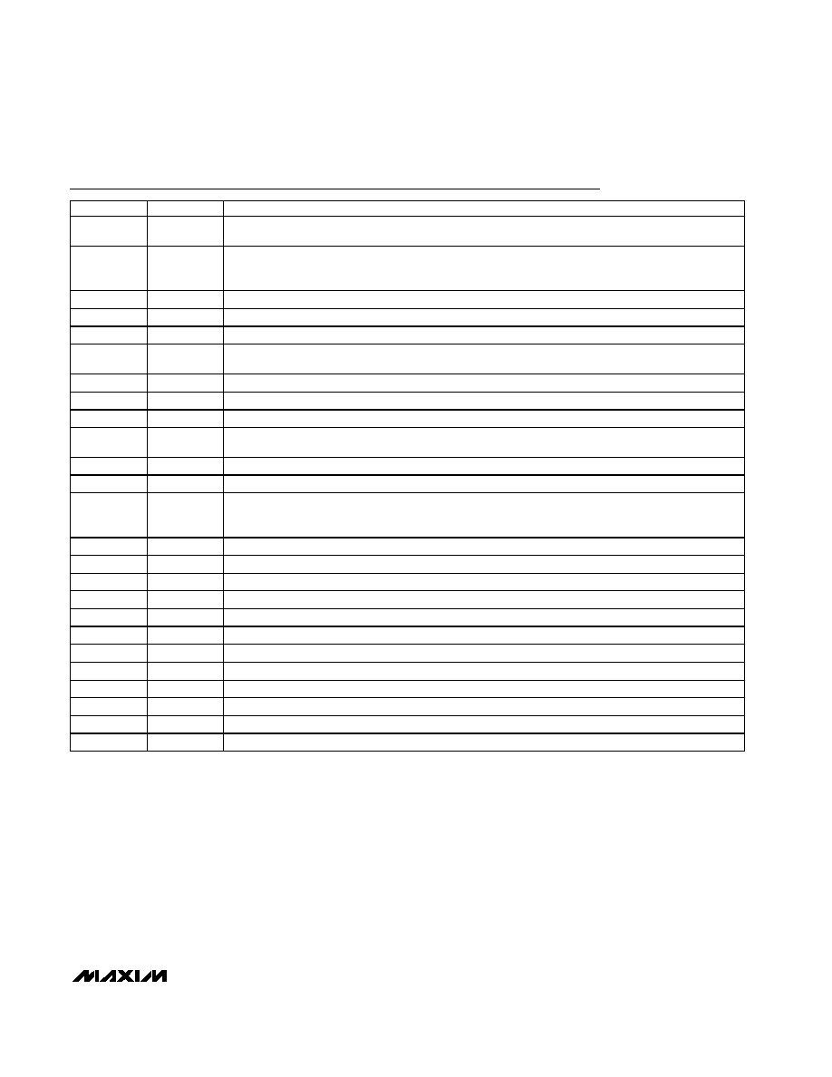
Pin Description
PIN
NAME
FUNCTION
1, 8
V
CC
Positive Supply Voltage. Bypass V
CC
to V
GG
with 0.1µF and 0.01µF ceramic capacitors. Place the
capacitors as close to the device as possible with the smaller value capacitor closest to the device.
2
SEL
Noninverting Differential Select Input. Setting SEL = 1 and
SEL = 0 enables all four channels to
operate independently. Setting SEL = 0 and
SEL = 1 enables all four channels to be synchronized to
CLK.
3
SEL
Inverting Differential Select Input
4
CLK
Noninverting Differential Clock Input
5
CLK
Inverting Differential Clock Input
6
EN
Noninverting Differential Output Enable Input. Setting EN = 1 and
EN = 0 enables all four outputs.
Setting EN = 0 and
EN = 1 disables all four outputs.
7
EN
Inverting Differential Output Enable Input
9
IN3
Noninverting Differential Input 3
10
IN3
Inverting Differential Input 3
11, 17, 24,
30
V
GG
Ground Reference
12
OUT3
Inverting Differential Output 3
13
OUT3
Noninverting Differential Output 3
14, 20, 21,
27
V
EE
Negative Supply Voltage. Bypass from V
EE
to V
GG
with 0.1µF and 0.01µF ceramic capacitors. Place
the capacitors as close to the device as possible with the smaller value capacitor closest to the
device.
15
IN2
Noninverting Differential Input 2
16
IN2
Inverting Differential Input 2
18
OUT2
Inverting Differential Output 2
19
OUT2
Noninverting Differential Output 2
22
OUT1
Noninverting Differential Output 1
23
OUT1
Inverting Differential Output 1
25
IN1
Inverting Differential Input 1
26
IN1
Noninverting Differential Input 1
28
OUT0
Noninverting Differential Output 0
29
OUT0
Inverting Differential Output 0
31
IN0
Inverting Differential Input 0
32
IN0
Noninverting Differential Input 0