 | –≠–ª–µ–∫—Ç—Ä–æ–Ω–Ω—ã–π –∫–æ–º–ø–æ–Ω–µ–Ω—Ç: MAX9513 | –°–∫–∞—á–∞—Ç—å:  PDF PDF  ZIP ZIP |

General Description
The MAX9513 CVBS video filter amplifier with
SmartSleep and bidirectional video support is ideal for
portable DVD players and portable media players
(PMPs). The input can be directly connected to the digi-
tal-to-analog converter (DAC) output. The reconstruction
filter removes high-frequency signals above 6.75MHz.
The amplifiers have 6dB of gain, and the outputs can be
DC-coupled to a load of 75, which is equivalent to two
video loads, or can be AC-coupled to a load of 150.
The SmartSleep circuitry intelligently reduces power
consumption based on the presence of the input signal
and the output loads. When the MAX9513 does not
detect the presence of sync on the input video signal,
the supply current is reduced to less than 7µA. The
device only enables a video amplifier when there is an
active video input signal and an attached load. The
video amplifier remains on while a load is connected. If
the load is disconnected, the video amplifier is turned off.
The MAX9513 contains one reconstruction filter, two
video amplifiers, and a pulldown switch at one of the
two CVBS outputs. The MAX9513 has the ability to con-
trol the bidirectional video signals at the CVBS video
connections without the need for separate switches or
relays. This feature is particularly useful for portable
DVD players, which often use the same connector to
drive a composite video output and to accept an exter-
nal video signal to display on the LCD panel.
The MAX9513 operates from a 2.7V to 3.6V single supply
and is offered in small 16-pin TQFN (3mm x 3mm) and
16-pin QSOP packages. The device is specified over
the -40∞C to +125∞C automotive temperature range.
Applications
Portable DVD Players
Portable Set-Top Boxes
Personal Video Recorders (PVRs)
Portable Media Players (PMPs)
Portable Video
Features
o SmartSleep Feature Detects Input Signal and
Output Load Status to Reduce Power
Consumption
o Standard-Definition Video Reconstruction Filter
with 6.75MHz Passband
o Two Composite Inputs and Outputs
o Integrated Support for a Bidirectional Composite
Video Signal
o Supports Two Video Loads at Each Output
(DC-Coupled)
o 2.7V to 3.6V Single-Supply Operation
MAX9513
CVBS Video Filter Amplifier with SmartSleep
and Bidirectional Video Support
_
__
__
__
__
__
__
__
__
__
__
__
__
__
__
__
__
__
__
__
__
__
__
__
__
__
__
__
__
__
__
__
__
__
__
__
__
__
__
__
__
__
__
__
__
__
__
__
__
__
__
__
__
__
__
__
__
__
__
__
__
__
__
__
_
Maxim Integrated Products
1
Ordering Information
19-0604; Rev 0; 7/06
For pricing, delivery, and ordering information, please contact Maxim/Dallas Direct! at
1-888-629-4642, or visit Maxim's website at www.maxim-ic.com.
E
EV
VA
AL
LU
UA
AT
TIIO
ON
N K
KIIT
T
A
AV
VA
AIIL
LA
AB
BL
LE
E
PART
PIN-PACKAGE PKG CODE
TOP MARK
MAX9513ATE+
16 TQFN-EP**
(3mm x 3mm)
T1633-4
AFC
MAX9513AEE+* 16 QSOP
E16-4
--
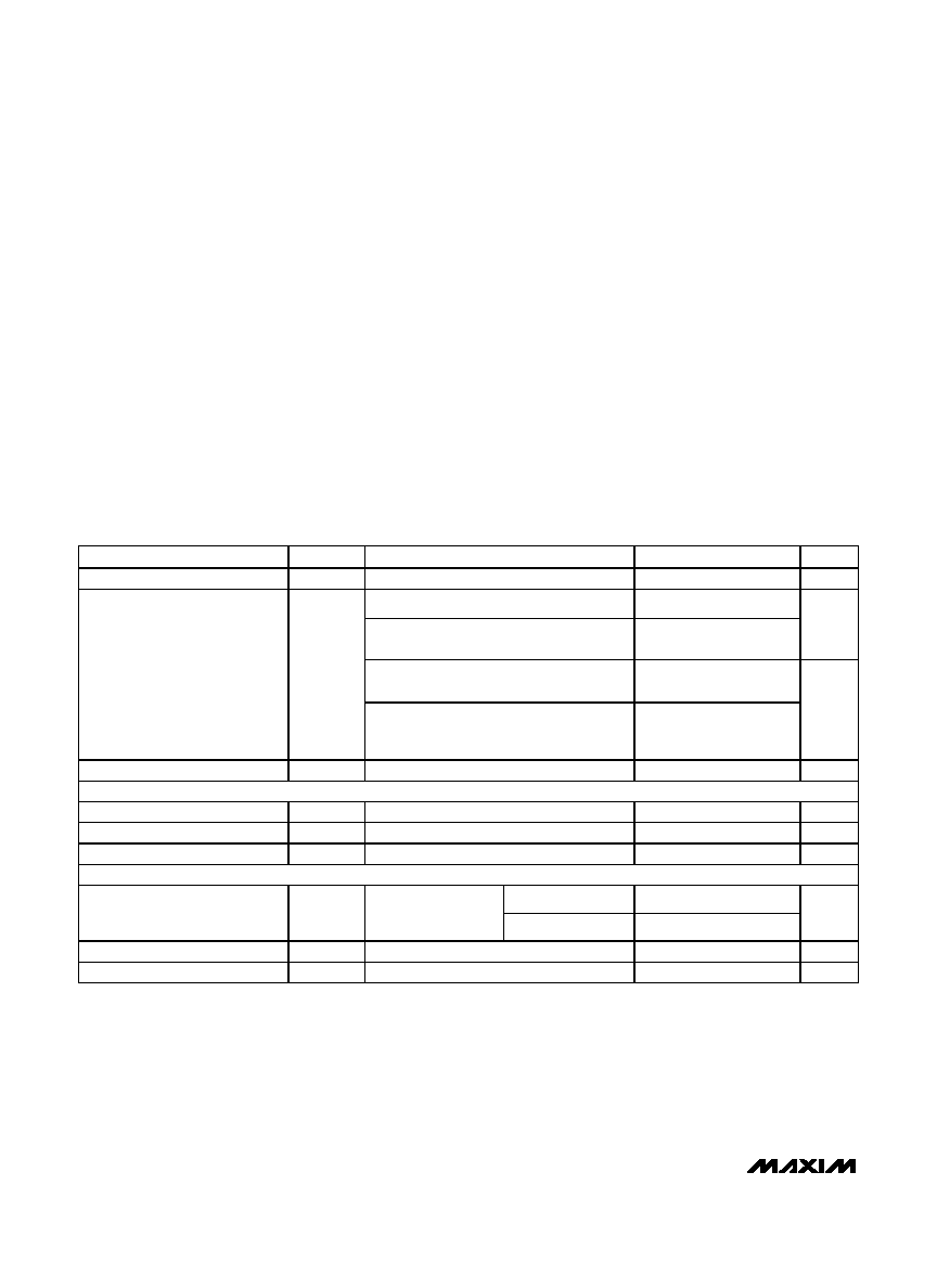
Block Diagrams
Note: All devices are specified over the -40∞C to +125∞C operat-
ing temperature range.
+
Denotes lead-free package.
*
Future product--contact factory for availability.
**
EP = Exposed pad.
EXTCVBSIN
CVBSOUT1
SHDN
INT/EXT
ACTIVE VIDEO
DETECT
SMARTSLEEP
CVBSIN
CVBSOUT2
CONTROL
LOGIC
CLAMP
BUFFER
LOAD SENSE
6dB
LOAD SENSE
6dB
LPF
MAX9513
Block Diagrams continued at end of data sheet.
MAX9513
CVBS Video Filter Amplifier with SmartSleep
and Bidirectional Video Support
2
_
__
__
__
__
__
__
__
__
__
__
__
__
__
__
__
__
__
__
__
__
__
__
__
__
__
__
__
__
__
__
__
__
__
__
__
__
__
__
__
__
__
__
__
__
__
__
__
__
__
__
__
__
__
__
__
__
__
__
__
__
__
__
__
__
__
__
__
__
__
__
__
__
__
__
__
__
__
__
__
__
__
__
__
__
__
__
_
A
AB
BS
SO
OL
LU
UT
TE
E M
MA
AX
XIIM
MU
UM
M R
RA
AT
TIIN
NG
GS
S
ELECTRICAL CHARACTERISTICS
(V
DD
= V
SHDN
= 3.3V, V
SMARTSLEEP
= V
INT/EXT
= GND = 0V, R
L
= no load. T
A
= T
MIN
to T
MAX
, unless otherwise noted. Typical val-
ues are at T
A
= +25∞C.) (Note 1)
Stresses beyond those listed under "Absolute Maximum Ratings" may cause permanent damage to the device. These are stress ratings only, and functional
operation of the device at these or any other conditions beyond those indicated in the operational sections of the specifications is not implied. Exposure to
absolute maximum rating conditions for extended periods may affect device reliability.
(Voltages with respect to GND.)
VDD ..........................................................................-0.3V to +4V
SMARTSLEEP, SHDN, INT/EXT,
CVBSIN, EXTCVBSIN ..........................................-0.3V to +4V
Duration of Short Circuit to
VDD or GND (CVBSOUT1, CVBSOUT2)................Continuous
Continuous Input Current
EXTCVBSIN, CVBSIN,
SMARTSLEEP, SHDN, INT/EXT ....................................±20mA
Continuous Power Dissipation (TA = +70∞C)
16-Pin TQFN (derate 15.6mW/∞C above +70∞C)..........1250mW
16-Pin QSOP (derate 8.3mW/∞C above +70∞C)...........667mW
Operating Temperature Range .........................-40∞C to +125∞C
Junction Temperature ......................................................+150∞C
Storage Temperature Range .............................-65∞C to +150∞C
Lead Temperature (soldering, 10s) .................................+300∞C
PARAMETER
SYMBOL
CONDITIONS
MIN
TYP
MAX
UNITS
Supply Voltage Range
V
DD
Guaranteed by PSRR
2.7
3.6
V
I NT /E X T = G N D , CVBSIN = 0.3V
13
16
INT/EXT = V
DD
,
EXTCVBSIN is unconnected
4.3
6
mA
SMARTSLEEP = V
DD,
CVBSIN has no active video signal
7
14
Supply Current
I
DD
SMARTSLEEP = V
DD
, CVBSIN has a black-
burst video signal with sync tip at GND
(Note 2)
17
µA
Shutdown Supply Current
I
SHDN
V
SHDN
= GND
0.01
10
µA
SMARTSLEEP CHARACTERISTICS
Minimum Line Frequency
CVBSIN
14.3
kHz
Sync Slice Level
CVBSIN
4.1
5.2
% V
DD
Output Load Detect Threshold
Sync pulse present, R
L
to GND
200
DC CHARACTERISTICS
2.7V < V
DD
< 3.6V
0
1.05
Input Voltage Range
V
IN
C V BS IN , g uar anteed
b y outp ut vol tag e
sw i ng
3.0V < V
DD
< 3.6V
0
1.2
V
Input Current
I
IN
CVBSIN = 0V
2
5
µA
Input Resistance
R
IN
CVBSIN
20
M
MAX9513
CVBS Video Filter Amplifier with SmartSleep
and Bidirectional Video Support
_
__
__
__
__
__
__
__
__
__
__
__
__
__
__
__
__
__
__
__
__
__
__
__
__
__
__
__
__
__
__
__
__
__
__
__
__
__
__
__
__
__
__
__
__
__
__
__
__
__
__
__
__
__
__
__
__
__
__
__
__
__
__
__
__
__
__
__
__
__
__
__
__
__
__
__
__
__
__
__
__
__
__
__
__
__
__
_
3
ELECTRICAL CHARACTERISTICS (continued)
(V
DD
= V
SHDN
= 3.3V, V
SMARTSLEEP
= V
INT/EXT
= GND = 0V, R
L
= no load. T
A
= T
MIN
to T
MAX
, unless otherwise noted. Typical val-
ues are at T
A
= +25∞C.) (Note 1)
PARAMETER
SYMBOL
CONDITIONS
MIN
TYP
MAX
UNITS
Sync-Tip Clamp Level
V
CLP
EXTCVBSIN
0.25
0.37
V
Inp ut C l am p i ng C ur r ent
EXTCVBSIN = 500mV + V
CLP
0.5
1
1.5
µA
2.7V < V
DD
< 3.6V
1.05
EXTCVBSIN Input Voltage Range
Guaranteed by
output voltage
swing
3.0V < V
DD
< 3.6V
1.2
V
P-P
Sync Crush
EXTCVBSIN, percentage reduction in sync
pulse (0.3V
P-P
), guaranteed by input
clamping current measurement, measured
at input
2
%
Maximum Input Source
Resistance
EXTCVBSIN
300
DC Voltage Gain
A
V
R
L
= 150
to V
DD
/ 2, 0V
V
IN
1.05V,
V
DD
= 2.7V
5.7
6
6.3
dB
DC Gain Matching
R
L
= 150
to V
DD
/ 2, 0V
V
IN
1.05V,
V
DD
= 2.7V
-0.2
0
+0.2
dB
CVBSIN = 0V,
INT/EXT = GND, R
L
= 150
to GND
0.21
0.3
0.38
Output Level
C
EXTCVBSIN
= 0.1µF to GND,
INT/EXT = V
DD,
R
L
= 150
to GND
0.21
0.27
0.38
V
T
A
= -40∞C to
+85∞C
2.027
2.1
2.163
Measured at output,
V
DD
= 2.7V,
0V
V
IN
1.05V,
R
L
= 150
to -0.2V
T
A
= -40∞C to
+125∞C
2.006
2.163
Measured at output, V
DD
= 2.7V,
0V
V
IN
1.05V, R
L
= 150
to V
DD
/ 2
2.027
2.1
2.163
T
A
= -40∞C to
+85∞C
2.316
2.4
2.472
Measured at output,
V
DD
= 3V,
0V
V
IN
1.2V,
R
L
= 150
to -0.2V
T
A
= -40∞C to
+125∞C
2.292
2.472
Measured at output, V
DD
= 3V,
0V
V
IN
1.2V, R
L
= 150
to V
DD
/ 2
2.316
2.4
2.472
Output Voltage Swing
Measured at output, V
DD
= 3.135V,
0V
V
IN
1.05V, R
L
= 75
to -0.2V
2.027
2.1
2.163
V
P-P
Output Resistance
R
OUT
V
OUT
= 1.3V, -5mA
I
LOAD
+5mA
0.47

MAX9513
CVBS Video Filter Amplifier with SmartSleep
and Bidirectional Video Support
4
_
__
__
__
__
__
__
__
__
__
__
__
__
__
__
__
__
__
__
__
__
__
__
__
__
__
__
__
__
__
__
__
__
__
__
__
__
__
__
__
__
__
__
__
__
__
__
__
__
__
__
__
__
__
__
__
__
__
__
__
__
__
__
__
__
__
__
__
__
__
__
__
__
__
__
__
__
__
__
__
__
__
__
__
__
__
__
_
ELECTRICAL CHARACTERISTICS (continued)
(V
DD
= V
SHDN
= 3.3V, V
SMARTSLEEP
= V
INT/EXT
= GND = 0V, R
L
= no load. T
A
= T
MIN
to T
MAX
, unless otherwise noted. Typical val-
ues are at T
A
= +25∞C.) (Note 1)
PARAMETER
SYMBOL
CONDITIONS
MIN
TYP
MAX
UNITS
Power-Supply Rejection Ratio
PSRR
2.7V
V
DD
3.6V, input referred,
R
L
= 150
to GND
48
dB
Output Pulldown Resistance
R
PD
INT/EXT = V
DD
, CVBSOUT1
3.7
Output Shutdown Impedance
28
k
LOGIC INPUTS (SMARTSLEEP,
SHDN, INT/EXT)
Logic-Low Threshold
V
IL
0.3 x
V
DD
V
Logic-High Threshold
V
IH
0.7 x
V
DD
V
Logic Input Current
I
IL
/ I
IH
V
I
= 0V or V
DD
0.01
10
µA
AC ELECTRICAL CHARACTERISTICS
(V
DD
= V
SHDN
= 3.3V, V
SMARTSLEEP
= V
INT/EXT
= GND = 0V, R
L
= 150 to GND. T
A
= T
MIN
to T
MAX
, unless otherwise noted. Typical
values are at T
A
= +25∞C.) (Note 1)
PARAMETER
SYMBOL
CONDITIONS
MIN
TYP
MAX
UNITS
f = 5.5MHz
-0.1
f = 6.75MHz
-1
-0.3
+1
f = 11MHz
-3
Standard-Definition
Reconstruction Filter
Inputs are 1V
P-P
, reference
frequency is 1MHz
f = 27MHz
-33
-41
dB
DC-coupled output,
5-step modulated staircase
f = 3.58MHz or
4.43MHz
0.2
Differential Gain
DG
AC-coupled output,
5-step modulated staircase
f = 3.58MHz or
4.43MHz
0.4
%
f = 3.58MHz
0.62
DC-coupled output,
5-step modulated staircase
f = 4.43MHz
0.75
f = 3.58MHz
0.78
Differential Phase
DP
AC-coupled output,
5-step modulated staircase
f = 4.43MHz
1.01
D eg r ees
2T Pulse Response
2T = 200ns or 250ns
0.2
K%
2T Bar Response
Bar time is 18µs, the beginning 2.5% and the ending 2.5%
of the bar time are ignored, 2T = 200ns or 250ns
0.2
K%
2T Pulse-to-Bar K
Rating
Bar time is 18µs, the beginning 2.5% and the ending 2.5%
of the bar time are ignored, 2T = 200ns or 250ns
0.3
K%

MAX9513
CVBS Video Filter Amplifier with SmartSleep
and Bidirectional Video Support
_
__
__
__
__
__
__
__
__
__
__
__
__
__
__
__
__
__
__
__
__
__
__
__
__
__
__
__
__
__
__
__
__
__
__
__
__
__
__
__
__
__
__
__
__
__
__
__
__
__
__
__
__
__
__
__
__
__
__
__
__
__
__
__
__
__
__
__
__
__
__
__
__
__
__
__
__
__
__
__
__
__
__
__
__
__
__
_
5
Note 1: All devices are 100% production tested at T
A
= +25∞C. Specifications over temperature limits are guaranteed by design.
Note 2: Specified current is an average over time.
AC ELECTRICAL CHARACTERISTICS (continued)
(V
DD
= V
SHDN
= 3.3V, V
SMARTSLEEP
= V
INT/EXT
= GND = 0V, R
L
= 150 to GND. T
A
= T
MIN
to T
MAX
, unless otherwise noted. Typical
values are at T
A
= +25∞C.) (Note 1)
PARAMETER
SYMBOL
CONDITIONS
MIN
TYP
MAX
UNITS
Nonlinearity
5-step staircase
0.1
%
Group Delay
Distortion
100kHz
f 5MHz, inputs are 1V
P-P
10
ns
Peak Signal to RMS
Noise
100kHz
f 5MHz, inputs are 1V
P-P
67
dB
Power-Supply
Rejection Ratio
f = 100kHz, 200mV
P-P
, input referred
43
dB
Output Impedance
f = 5MHz
6
Enable Time
CVBSIN = 1V, output settled to within 1% of the final
voltage, R
L
= 150
to GND
13
µs
Disable Time
CVBSIN = 1V, output settled to within 1% of the final
voltage, R
L
= 150
to GND
1.1
µs
CROSSTALK
All Hostile Output
Crosstalk
f = 4.43MHz
-70
dB
All Hostile Input
Crosstalk
f = 4.43MHz,
SHDN = GND,
input termination resistors are 75
-69
dB